/filters:background_color(white)/2024-03/LWB5-Plus-Modules-And-USB1.png)
Introduction
Overview
This document describes key hardware aspects of the Sterling-LWB5+ USB Adapter. This document is intended to assist device manufacturers and related parties with the integration of this radio into their host devices. Data in this document is drawn from several sources. For full documentation on the Sterling-LWB5+, visit:
General Description
The LWB5+ wireless USB adapter is an integrated, small form factor 1x1 SISO 802.11 a/b/g/n/ac WLAN plus Bluetooth® 5.2 dual mode USB adaptor that is optimized for low-power mobile devices. The integration of all WLAN and Bluetooth functionality in a single package supports low cost and easy use.
The adaptor is pre-calibrated and contains the complete transmit/receive RF paths including diplexer, switches, ceramic chip antenna, reference crystal oscillator, slow clock oscillator and power management unit (PMU).
The LWB5+ wireless adaptor supports IEEE 802.11ac 1x1 SISO with data rates up to MCS9 (433.3 Mbps). An internal Wi-Fi and Bluetooth coexistence scheme provides optimized connectivity while Wi-Fi and Bluetooth are operating simultaneously. The device’s low power consumption radio architecture and power management unit (PMU) proprietary power save technologies allow for extended battery life.
In addition, its dual 802.11ac and Bluetooth radio includes full digital MAC and baseband engines that handle all 802.11 CCK/OFDM® 2.4/5 GHz and Bluetooth 5.2 (Basic Rate, Enhanced Data Rate, and Bluetooth Low Energy) baseband and protocol processing.
This datasheet is subject to change. Please contact Ezurio for further information.
Features & Benefits
The Sterling-LWB5+ USB Adapter features and benefits are described in the following table.
| Feature | Description |
|---|---|
| Radio Front End |
|
| Power Management | High efficiency buck regulator converts USB VBUS 5.0V to 3.3V for the CYW4373E chip. One buck regulator, multiple LDO regulators, and a power management unit (PMU) are integrated into the CYW4373E. All regulators are programmable via the PMU. These blocks simplify power supply design for Bluetooth and WLAN functions in embedded designs. |
| Pre-Calibration | RF system tested and calibrated in production |
| Sleep Clock | Built in 32.768 kHz oscillator |
| Host Interface | An on-chip USB 2.0 hub provides a single shared USB connection to both WLAN and Bluetooth target devices. |
| Advanced WLAN |
|
| Advanced Bluetooth |
|
Specification Summary
Processor / SoC / Chipset
| Wireless | Infineon CYW4373E |
Wi-Fi
| Standards | IEEE 802.11a, 802.11b, 802.11e, 802.11g, 802.11h, 802.11i, 802.11k*, 802.11n, 802.11r, 802.11v*, 802.11ac |
| Interface | USB 2.0 |
| Frequency Range | |
| Spatial Streams | 1 (1x1 SISO) [802.11ac/n] |
| Channel Support | 2.4 GHz
5 GHz:
|
| Supported Data Rates | Support 802.11 ac/a/b/g/n 1x1 SISO. 802.11b (DSSS, CCK) 1, 2, 5.5, 11 Mbps 802.11a/g (OFDM) 6, 9, 12, 18, 24, 36, 48, 54 Mbps 802.11n (OFDM, HT20/HT40, MCS0-7) 802.11ac (OFDM, VHT20, MCS0-8; OFDM, VHT40/HT80, MCS0-9) |
| Modulation Schemes | BPSK, QPSK, CCK, 16-QAM, 64-QAM, and 256-QAM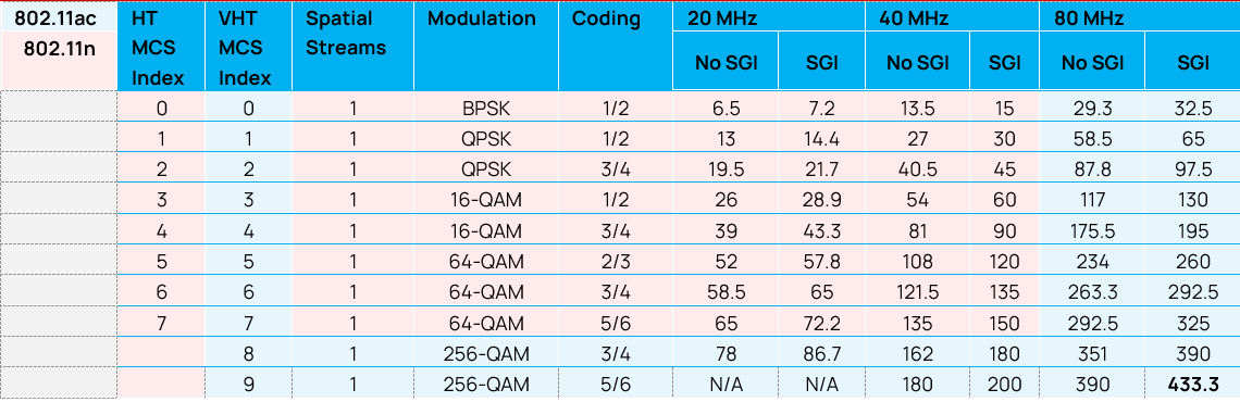 |
| Network Architecture Type | Infrastructure (client operation), Access Point |
| Wi-Fi Media | Direct Sequence-Spread Spectrum (DSSS) Complementary Code Keying (CCK) Orthogonal Frequency Divisional Multiplexing (OFDM) |
| Wi-Fi Multimedia | WMM Wi-Fi Multimedia - PowerSave (WMM-PS with U-APSD) WMM-Sequential Access (WMM-SA with PCF) |
| Coexistence |
Bluetooth
| Standards | Bluetooth 5.2 Core Spec |
| Interface | USB 2.0 |
| Supported Data Rates | 1, 2, 3 Mbps |
| Bluetooth Modulation | GFSK@ 1 Mbps Pi/4-DQPSK@ 2 Mbps 8-DPSK@ 3 Mbps |
| Bluetooth Media | Frequency Hopping Spread Spectrum (FHSS) |
Radio Performance
| Tx Power (conducted, measured at output of embedded module)
Note: Transmit power on each channel varies per individual country regulations. All values are nominal with +/-2 dBm tolerance at room temperature. Tolerance could be up to +/-2.5 dBm across operating temperature. Note: HT40 – 40 MHz-wide channels HT80 – 80 MHz-wide channels | 802.11a
802.11b
802.11g
802.11n (2.4 GHz)
802.11n (5 GHz)
802.11ac (5 GHz)
Bluetooth
|
RX Sensitivity (conductive) (PER <= 10%) Note: All values nominal, +/-3 dBm. | 802.11a:
802.11b:
802.11g:
802.11n (2.4 GHz):
802.11n (5 GHz):
802.11ac (5 GHz):
Bluetooth:
|
| 2.4 GHz Frequency Bands |
|
| 5 GHz Frequency Bands | EU
FCC
ISED
MIC
RCM
|
Interfaces
| Physical Interfaces | USB 2.0 Type-A connector |
| Network Interfaces | Wi-Fi: USB 2.0 Bluetooth: USB 2.0 |
Power
| Input Voltage | Operational: USB Vbus 5.0V+/-10% |
Mechanical
| Dimensions | Length: 47 (1.85) Width: 17.5 (0.89) Thickness: 11.7 (0.46) |
| Weight | ~7g (0.25) |
Software
| OS Support | Linux Android |
| Security |
|
Environmental
| Operating Temperature | -40° to +85°C (-40° to +185°F) |
| Storage Temperature | -40° to +85°C (-40° to +185°F) |
| Operating Humidity | 10 to 90% (non-condensing) |
| Storage Humidity | 10 to 90% (non-condensing) |
| MSL (Moisture Sensitivity Level) | 3 |
| Maximum Electrostatic Discharge | Conductive 4KV; Air coupled 8KV (follow EN61000-4-2) |
| Lead Free | Lead-free and RoHS Compliant |
Certifications
| Regulatory Compliance | United States (FCC) EU - Member countries of European Union (ETSI) ISED (Canada) Australia Japan |
| Compliance Standards | EU
FCC
ISED Canada
AS/NZS
MIC
|
| Bluetooth SIG | Bluetooth® SIG Qualification |
Warranty
| Warranty Terms | One Year Warranty |
Functional Descriptions
WLAN Functional Description
The LWB5+ wireless USB adaptor is designed based on the Cypress CYW4373EUBGT 802.11ac/a/b/g/n chipset. It is optimized for high speed, reliability, and low-power embedded applications. It is integrated with dual-band WLAN (2.4/5 GHz) and Bluetooth 5.2. Its functionality includes the following:
- Improved throughput on the link due to frame aggregation, RIFS (reduced inter-frame spacing), and half guard intervals.
- Support for LDPC (Low Density Parity Check) codes.
- Improved 11n performance due to features such as 11n frame aggregation (TX A-MPDU) and low-overhead host-assisted buffering (RX A-MPDU). These techniques can improve performance and efficiency of applications involving large bulk data transfers such as file transfers or high-resolution video streaming.
- IEEE 802.11ac, 1x1 SISO with data rate up to MCS9 (433.3 Mbps).
Additional functionality is listed below.
| Feature | Description | ||||||||||||||||||||||||||||||||||||||||||||||||||||||||||||||||||||||||||||||||||||||||||||||||||||||||||||||||||||||||||||||||||||||||||||||||||||||||||||||||||||||||||||||||||||||||||||||||||||||||||||||||||||||||
|---|---|---|---|---|---|---|---|---|---|---|---|---|---|---|---|---|---|---|---|---|---|---|---|---|---|---|---|---|---|---|---|---|---|---|---|---|---|---|---|---|---|---|---|---|---|---|---|---|---|---|---|---|---|---|---|---|---|---|---|---|---|---|---|---|---|---|---|---|---|---|---|---|---|---|---|---|---|---|---|---|---|---|---|---|---|---|---|---|---|---|---|---|---|---|---|---|---|---|---|---|---|---|---|---|---|---|---|---|---|---|---|---|---|---|---|---|---|---|---|---|---|---|---|---|---|---|---|---|---|---|---|---|---|---|---|---|---|---|---|---|---|---|---|---|---|---|---|---|---|---|---|---|---|---|---|---|---|---|---|---|---|---|---|---|---|---|---|---|---|---|---|---|---|---|---|---|---|---|---|---|---|---|---|---|---|---|---|---|---|---|---|---|---|---|---|---|---|---|---|---|---|---|---|---|---|---|---|---|---|---|---|---|---|---|---|---|---|
| WLAN MAC |
| ||||||||||||||||||||||||||||||||||||||||||||||||||||||||||||||||||||||||||||||||||||||||||||||||||||||||||||||||||||||||||||||||||||||||||||||||||||||||||||||||||||||||||||||||||||||||||||||||||||||||||||||||||||||||
| WLAN Security |
| ||||||||||||||||||||||||||||||||||||||||||||||||||||||||||||||||||||||||||||||||||||||||||||||||||||||||||||||||||||||||||||||||||||||||||||||||||||||||||||||||||||||||||||||||||||||||||||||||||||||||||||||||||||||||
| WLAN Channel | Channel frequency supported.
· | ||||||||||||||||||||||||||||||||||||||||||||||||||||||||||||||||||||||||||||||||||||||||||||||||||||||||||||||||||||||||||||||||||||||||||||||||||||||||||||||||||||||||||||||||||||||||||||||||||||||||||||||||||||||||
Bluetooth Functional Description
The LWB5+ wireless USB adaptor includes a fully integrated Bluetooth baseband/radio. Several features and functions are listed below.
| Feature | Description |
|---|---|
| Bluetooth Interface | USB 2.0 |
| Bluetooth Core functionality |
|
| Bluetooth Low Energy (BLE) Core functionality |
|
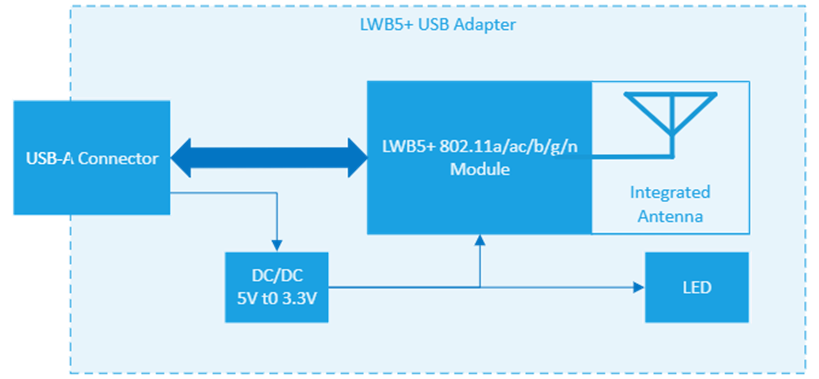
Hardware Architecture
Block Diagrams
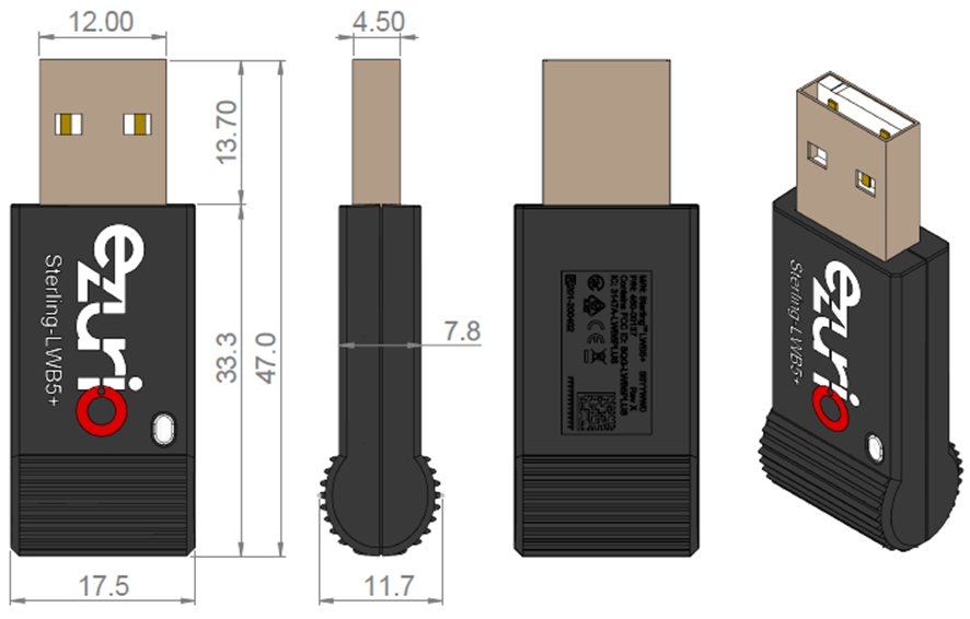
Mechanical Drawings
LWB5+ USB Adapter dimensions is 47 x 17.5 x 11.7 mm.
Notes:
The Wi-Fi MAC address is located on the product label.
The last digit of Wi-Fi MAC address is assigned to either 0, 2, 4, 6, 8, A, C, E.
The Bluetooth MAC address is the Wi-Fi MAC address plus 1.
Host Interface Specifications
USB LS Driver and Receiver Parameters
Notes:
Over full range of values specified in the Recommended Operating Conditions unless otherwise specified.
The load is 100Ω differential for these parameters, unless other specified.
| Symbol | Parameter | Min. | Typ. | Max. | Unit |
|---|---|---|---|---|---|
| BR | Baud rate | - | 1.5 | - | Mbps |
| BRPPM | Baud rate tolerance | -15000 | - | 15000 | ppm |
| Driver Specifications | |||||
| VOH | Output signal ended high Defined with 1.425KΩ pull-up resistor to 3.6V | 2.8 | - | 3.6 | V |
| VOL | Output signal ended low Defined with 1.425KΩ pull-up resistor to ground | 0.0 | - | 0.3 | V |
| VCRS | Output signal crossover voltage | 1.3 | 2.0 | V | |
| TLR | Data fall time Defined from 10% to 90% for raise time and 90% to 10% for fall time | 75.0 | - | 300.0 | ns |
| TLF | Data rise time Defined from 10% to 90% for raise time and 90% to 10% for fall time | 75.0 | - | 300.0 | ns |
| TLRFM | Rise and fall time matching | 80.0 | - | 125.0 | % |
| TUDJ1 | Source jitter total: to next transition *Including frequency tolerance. Timing difference between the differential data signals. *Defined at crossover point of differential signals | -95 | - | 95 | ns |
| TUDJ2 | Source jitter total: for paired transitions *Including frequency tolerance. Timing difference between the differential data signals. *Defined at crossover point of differential signals | -150 | - | 150 | ns |
| Receiver Specifications | |||||
| VIH | Input signal ended high | 2.0 | - | - | V |
| VIL | Input signal ended low | - | - | 0.8 | V |
| VDI | Differential input sensitivity | 0.2 | - | - | V |
USB FS Driver and Receiver Parameters
Notes:
Over full range of values specified in the Recommended Operating Conditions unless otherwise specified.
The load is 100Ω differential for these parameters, unless other specified.
| Symbol | Parameter | Min. | Typ. | Max. | Unit |
|---|---|---|---|---|---|
| BR | Baud rate | - | 12.0 | - | Mbps |
| BRPPM | Baud rate tolerance | -2500 | - | 2500 | ppm |
| Driver Specifications | |||||
| VOH | Output signal ended high Defined with 1.425KΩ pull-up resistor to 3.6V | 2.8 | - | 3.6 | V |
| VOL | Output signal ended low Defined with 1.425KΩ pull-up resistor to ground | 0.0 | - | 0.3 | V |
| VCRS | Output signal crossover voltage | 1.3 | 2.0 | V | |
| TFR | Output raise time Defined from 10% to 90% for raise time and 90% to 10% for fall time | -4.0 | - | 20.0 | ns |
| TFL | Output fall time Defined from 10% to 90% for raise time and 90% to 10% for fall time | -4.0 | - | 20.0 | ns |
| TDJ1 | Source jitter total: to next transition *Including frequency tolerance. Timing difference between the differential data signals. *Defined at crossover point of differential signals | -3.5 | - | 3.5 | ns |
| TDJ2 | Source jitter total: for paired transitions *Including frequency tolerance. Timing difference between the differential data signals. *Defined at crossover point of differential signals | -4.0 | - | 4.0 | ns |
| TFDEOP | Source jitter for differential transition to SE0 transition. Defined at crossover point of differential signals | -2.0 | - | 5.0 | ns |
| Receiver Specifications | |||||
| VIH | Input signal ended high | 2.0 | - | - | V |
| VIL | Input signal ended low | - | - | 0.8 | V |
| VDI | Differential input sensitivity | 0.2 | - | - | V |
| TJR1 | Receiver jitter: to next transition Defined at crossover point of differential data signals | -18.5 | - | 18.5 | ns |
| TJR2 | Receiver jitter: for paired transitions Defined at crossover point of differential data signals | -9.0 | - | 9.0 | ns |
USB HS Driver and Receiver Parameters
Notes:
Over full range of values specified in the Recommended Operating Conditions unless otherwise specified.
The load is 100Ω differential for these parameters, unless other specified.
| Symbol | Parameter | Min. | Typ. | Max. | Unit |
|---|---|---|---|---|---|
| BR | Baud rate | - | 480 | - | Mbps |
| BRPPM | Baud rate tolerance | -500 | - | 500 | ppm |
| Driver Specifications | |||||
| VHSOH | Data signal high | 360 | - | 440 | mV |
| VHSOL | Data signal low | -10 | - | 10 | mV |
| THSR | Data rise time Defined from 10% to 90% for raise time and 90% to 10% for fall time | 500 | - | - | ns |
| THSF | Data fall time Defined from 10% to 90% for raise time and 90% to 10% for fall time | -500 | - | - | ns |
| Receiver Specifications | |||||
| VHSCM | Input signal ended low | -50 | - | 500 | mV |
Electrical Characteristics
Absolute Maximum Ratings
The following table summarizes the absolute maximum ratings for the LWB5+ series wireless module. Absolute maximum ratings are those values beyond which damage to the device can occur. Functional operation under these conditions, or at any other condition beyond those indicated in the operational sections of this document, is not recommended.
Note: Maximum rating for signals follows the supply domain of the signals.
| Symbol (Domain) | Parameter | Max Rating | Unit |
|---|---|---|---|
| USB_VBUS | External DC power supply from USB VBUS | 5.5 | V |
| Storage | Storage temperature | -40 to +85 | °C |
| ESD | Electrostatic discharge tolerance | 2000 | V |
Recommended Operating Conditions
The following table lists the recommended operating conditions for the LWB5+ series wireless module.
| Symbol (Domain) | Parameter | Min | Typ | Max | Unit |
|---|---|---|---|---|---|
| USB_VBUS | External DC power supply from USB VBUS | 4.5 | 5.0 | 5.5 | V |
| T-ambient | Ambient temperature Note 1 | -40 | 25 | 85 | °C |
Notes:
Note 1: When ambient temperature is higher than +65 degree C, the thermal throttling algorithm may be enabled and reduce the transmit duty cycle to lower the heat generated by the chip. Throughput will drop accordingly.
Radio Characteristics
WLAN Radio Receiver Characteristics
The following tables summarize the LWB5+ wireless USB adaptor receiver characteristics.
WLAN receiver conductive characteristics for 2.4 GHz single chain operation
| Symbol | Parameter | Conditions | Min | Typ | Max | Unit |
|---|---|---|---|---|---|---|
| Frx | Receive input frequency range | — | 2.412 | — | 2.484 | GHz |
| Srf | Sensitivity | |||||
| CCK, 1 Mbps | See Note1 | — | -95 | — | dBm | |
| CCK, 11 Mbps | — | -90 | — | |||
| OFDM, 6 Mbps | — | -92 | — | |||
| OFDM, 54 Mbps | — | -75 | — | |||
| HT20, MCS0 | — | -91 | — | |||
| HT20, MCS7 | — | -73 | — | |||
| HT40, MCS0 | — | -90 | — | |||
| HT40, MCS7 | — | -71 | — | |||
| Radj | Adjacent channel rejection | |||||
| OFDM, 6 Mbps | See Note1 | 16 | 38 | — | dB | |
| OFDM, 54 Mbps | -1 | 20.4 | — | |||
| HT20, MCS0 | 16 | 33.3 | — | |||
| HT20, MCS7 | -2 | 13.7 | — | |||
WLAN receiver conductive characteristics for 5 GHz single chain operation
| Symbol | Parameter | Conditions | Min | Typ | Max | Unit |
|---|---|---|---|---|---|---|
| Frx | Receive input frequency range | — | 5.15 | — | 5.825 | GHz |
| Srf | Sensitivity | |||||
| OFDM, 6 Mbps | See Note1 | — | -92 | — | dBm | |
| OFDM, 54 Mbps | — | -74 | — | |||
| HT20, MCS0 | — | -91 | — | |||
| HT20, MCS7 | — | -73 | — | |||
| HT40, MCS0 | — | -89 | — | |||
| HT40, MCS7 | — | -69 | — | |||
| VHT20, MCS0 | — | -90 | — | |||
| VHT20, MCS8 | — | -67 | — | |||
| VHT40, MCS0 | — | -89 | — | |||
| VHT40, MCS9 | — | -63 | — | |||
| VHT80, MCS0 | — | -85 | — | |||
| VHT80, MCS9 | — | -60 | — | |||
Radj [Difference between interfering and desired signal (20 MHz apart)] | Adjacent channel rejection | |||||
| OFDM, 6 Mbps | See Note1 | 16 | 31.7 | — | dB | |
| OFDM, 54 Mbps | -1 | 13.8 | — | |||
| OFDM, 65 Mbps | -2 | 8.4 | — | |||
Radj. [Difference between interfering and desired signal (40 MHz apart)] | OFDM, 6 Mbps | See Note1 | 32 | 44.7 | — | dB |
| OFDM, 54 Mbps | 15 | 26.6 | — | |||
| OFDM, 65 Mbps | 14 | 26.8 | — | |||
Note1: Performance data are measured under signal chain operation.
Note: All the conductive measurements are carried out by installing a MHF4 connector on the module reference to the LWB5+ (453-00046R)
WLAN Transmitter Characteristics
WLAN transmitter conductive characteristics for 2.4 GHz operation
| Symbol | Parameter | Conditions | Min | Typ | Max | Unit |
|---|---|---|---|---|---|---|
| Ftx | Transmit output frequency range | — | 2.402 | — | 2.484 | GHz |
| Pout | Output power | See Note2 | — | — | — | — |
| 11b mask compliant | 1-11Mbps | — | 18 | — | dBm | |
| 11g mask compliant | 6-36Mbps | — | 18 | — | ||
| 11g EVM compliant | 48-54Mbps | — | 18 | — | ||
| 11n HT20 mask compliant | MCS0-6 | — | 18 | — | ||
| 11n HT20 EVM compliant | MCS7 | — | 17.5 | — | ||
| 11n HT40 mask compliant | MCS0-5 | — | 18 | — | ||
| 11n HT40 EVM compliant | MCS6-7 | — | 16.5 | — | ||
| ATx | Transmit power accuracy at 25 ℃ | — | -2.0 | — | +2.0 | dB |
WLAN current consumption on 2.4 GHz operation@25 degree C
| Freq. | Mode/Rate (Mbps) | Output Power (dBm) | Maximum Current Consumption @ USB VBUS (mA) |
|---|---|---|---|
2412 MHz 2422 MHz | 1 Mbps | 18 dBm | 288 |
| 54 Mbps | 18 dBm | 280 | |
| HT20 MCS7 | 17.5 dBm | 290 | |
| HT40 MCS7 | 16.5 dBm | 295 | |
| 2442 MHz | 1 Mbps | 18 dBm | 290 |
| 54 Mbps | 17 dBm | 278 | |
| HT20 MCS7 | 17 dBm | 290 | |
| HT40 MCS7 | 16 dBm | 300 | |
2472 MHz 2462 MHz | 1 Mbps | 18 dBm | 290 |
| 54 Mbps | 17 dBm | 280 | |
| HT20 MCS7 | 17 dBm | 287 | |
| HT40 MCS7 | 16 dBm | 298 |
WLAN transmitter conductive characteristics for 5 GHz operation
| Symbol | Parameter | Conditions | Min | Typ | Max | Unit |
|---|---|---|---|---|---|---|
| Ftx | Transmit output frequency range | — | 5.15 | — | 5.925 | GHz |
| Pout | Output power | See Note2 | — | — | — | — |
| 11a mask compliant | 6-36Mbps | — | 17.5 | — | dBm | |
| 11a EVM compliant | 48-54Mbps | — | 17.5 | — | ||
| 11n HT20 mask compliant | MCS0-5 | — | 17.5 | — | ||
| 11n HT20 EVM compliant | MCS6-7 | — | 16.5 | — | ||
| 11n HT40 mask compliant | MCS0-5 | — | 17.5 | — | ||
| 11n HT40 EVM compliant | MCS6-7 | — | 16 | — | ||
| 11ac VHT20 mask compliant | MCS0-5 | — | 17.5 | — | ||
| 11ac VHT20 EVM compliant | MCS6-8 | — | 15 | — | ||
| 11ac VHT40 mask compliant | MCS0-5 | — | 17.5 | — | ||
| 11ac VHT40 EVM compliant | MCS6-7 | — | 16 | — | ||
| 11ac VHT40 EVM compliant | MCS8-9 | — | 13.5 | — | ||
| 11ac VHT80 mask compliant | MCS0-5 | — | 17.5 | — | ||
| 11ac VHT80 EVM compliant | MCS6-7 | — | 16 | — | ||
| 11ac VHT80 EVM compliant | MCS8-9 | — | 13.5 | — | ||
| ATx | Transmit power accuracy at 25 ℃ | — | -2.0 | — | +2.0 | dB |
WLAN current consumption on 5 GHz operation@ 25 degree C
| Frequency (MHz) | Mode/Rate (Mbps) | Output Power (dBm) | Maximum Current Consumption @ USB VBUS(mA) |
|---|---|---|---|
| 5180 | 6 Mbps | 17.5 | 295 |
| 54 Mbps | 17.5 | 280 | |
| HT20 MCS0 | 17.5 | 288 | |
| HT20 MCS7 | 16.5 | 275 | |
| 5190 | HT40 MCS0 | 17.5 | 335 |
| HT40 MCS7 | 16 | 315 | |
| 5210 | VHT80 MCS0 | 17.5 | 345 |
| VHT80 MCS9 | 13.5 | 290 | |
| 5500 | 6 Mbps | 17.5 | 298 |
| 54 Mbps | 17.5 | 282 | |
| HT20 MCS0 | 17.5 | 287 | |
| HT20 MCS7 | 16.5 | 277 | |
| 5510 | HT40 MCS0 | 17.5 | 340 |
| HT40 MCS7 | 16 | 318 | |
| 5530 | VHT80 MCS0 | 17.5 | 350 |
| VHT80 MCS9 | 13.5 | 295 | |
| 5825 | 6 Mbps | 17.5 | 293 |
| 54 Mbps | 17.5 | 284 | |
| HT20 MCS0 | 17.5 | 287 | |
| HT20 MCS7 | 16.5 | 279 | |
| 5795 | HT40 MCS0 | 17.5 | 344 |
| HT40 MCS7 | 16 | 320 | |
| 5775 | VHT80 MCS0 | 17.5 | 355 |
| VHT80 MCS9 | 13.5 | 300 |
Note2: Final TX power values on each channel are limited by regulatory requirements.
Note: All the conductive measurements are carried out by installing a MHF4 connector on the module reference to the LWB5+ (453-00046R)
Bluetooth Receiver Characteristics
The following tables describe the basic rate receiver performance and enhanced rate receiver performance at 25°C.
Basic rate receiver performance temperature at 25°C
| Test Parameter | Min | Typ | Max | Bluetooth Spec. | Unit | |
|---|---|---|---|---|---|---|
| Sensitivity (1DH5) | BER ≤ 0.1% | — | -91 | — | ≤ -70 | dBm |
| Maximum Input | BER ≤ 0.1% | — | — | -20 | ≥ -20 | dBm |
| Interference Performance | Co-Channel | — | 9 | 11 | 11 | dB |
| C/I 1 MHz adjacent channel | — | -5.5 | 0 | 0 | dB | |
| C/I 2 MHz adjacent channel | — | -38 | -30 | -30 | dB | |
| C/I ≥ 3 MHz adjacent channel | — | -46 | -40 | -40 | dB | |
| C/I image channel | — | -25.5 | -9 | -9 | dB | |
| C/I 1-MHz adjacent to image channel | — | -39 | -20 | -20 | dB | |
Enhanced data rate receiver performance
| Test Parameter | Min | Typ | Max | Bluetooth Spec. | Unit | |
|---|---|---|---|---|---|---|
| Sensitivity (BER ≤ 0.01%) | π/4-DQPSK | — | -93 | — | ≤ -70 | dBm |
| 8-DPSK | — | -87 | — | ≤ -70 | dBm | |
| Maximum Input (BER ≤ 0.1%) | π/4-DQPSK | — | — | -20 | ≥ -20 | dBm |
| 8-DPSK | — | — | -20 | ≥ -20 | dBm | |
| C/I Co-Channel (BER ≤ 0.1%) | π/4-DQPSK | — | 10.5 | 13 | ≤ ±13 | dB |
| 8-DPSK | — | 17.5 | 21 | ≤ ±21 | dB | |
| C/I 1 MHz adjacent Channel | π/4-DQPSK | — | -6 | 0 | ≤ 0 | dB |
| 8-DPSK | — | -3 | 5 | ≤5 | dB | |
| C/I 2 MHz adjacent Channel | π/4-DQPSK | — | -38.5 | -30 | ≤ -30 | dB |
| 8-DPSK | — | -37.5 | -25 | ≤ -25 | dB | |
| C/I ≥ 3 MHz adjacent Channel | π/4-DQPSK | — | -47 | -40 | ≤ -40 | dB |
| 8-DPSK | — | -39.5 | -33 | ≤ -33 | dB | |
| C/I image channel | π/4-DQPSK | — | -24.5 | -7 | ≤ -7 | dB |
| 8-DPSK | — | -17 | 0 | ≤ 0 | dB | |
| C/I 1 MHz adjacent to image channel | π/4-DQPSK | — | -43 | -20 | ≤ -20 | dB |
| 8-DPSK | — | -37 | -13 | ≤ -13 | dB | |
Out-of-Band Blocking Performance (CW) BER ≤ 0.1% | 30-2000MHz | — | -10 | — | — | dBm |
| 2-2.399GHz | — | -27 | — | — | dBm | |
| 2.484-3GHz | — | -27 | — | — | dBm | |
| 3-12.75GHz | — | -10 | — | — | dBm | |
Bluetooth Transmitter Characteristics
The following tables describe the basic rate transmitter performance, basic rate receiver performance, enhanced rate receiver performance, and current consumption conditions at 25°C.
Basic rate transmitter performance temperature at 25°C
| Test Parameter | Min | Typ | Max | BT Spec. | Unit | ||
|---|---|---|---|---|---|---|---|
| Maximum RF Output Power | GFSK | — | — | 7 | 0 ~ +20 | dBm | |
| π/4-DQPSK | — | 3 | — | ||||
| 8-DPSK | — | 3 | — | ||||
| Frequency Range | 2.4 | — | 2.4835 | 2.4 ≤ f ≤ 2.4835 | GHz | ||
| 20 dB Bandwidth | — | 919.5 | — | ≤ 1000 | KHz | ||
| Δf1avg Maximum Modulation | 140 | 155 | 175 | 140 < Δf1avg < 175 | KHz | ||
| Δf2max Minimum Modulation | 115 | 135 | — | ≥ 115 | KHz | ||
| Δf2avg/Δf1avg | — | 0.9 | — | ≥ 0.80 | — | ||
| Initial Carrier Frequency | — | ± 25 | ± 75 | ≤ ± 75 | KHz | ||
| Frequency Drift (DH1 packet) | — | ± 10 | ± 25 | ± 25 | KHz | ||
| Frequency Drift (DH3 packet) | — | ± 10 | ± 40 | ± 40 | KHz | ||
| Frequency Drift (DH5 packet) | — | ± 10 | ± 40 | ± 40 | KHz | ||
| Drift rate | — | 8 | 20 | 20 | KHz/50us | ||
| Adjacent Channel Power | F ≥ ± 3 MHz | — | -50 | — | < -40 | dBm | |
| F = ± 2 MHz | — | -46 | — | ≤ -20 | dBm | ||
| F = ± 1 MHz | — | -15 | — | N/A | dBm | ||
BLE RF Specifications
| Parameter | Conditions | Min | Typ | Max | Unit |
|---|---|---|---|---|---|
| Frequency range | — | 2402 | — | 2480 | MHz |
| Rx sensitivity3 | GFSK, 30.8% PER, 1Mbps | — | -94 | — | dBm |
| Tx power | — | — | — | 7 | dBm |
| Δf1 average | — | 225 | 255 | 275 | KHz |
| Δf2 maximum4 | — | 185 | 220 | — | KHz |
| ratio | — | 0.8 | 0.95 | — | — |
Note3: Dirty Tx is Off.
Note4: At least 99.9% of all Δf2 maximum frequency values recorded over 10 packets must be greater than 185 KHz.
Bluetooth current consumption @ USB VBUS
| Mode | Current (mA) Tx Min | Current (mA) Tx Avg | Current (mA) Tx Max | Current (mA) Rx Min | Current (mA) Rx Avg | Current (mA) Rx Max |
|---|---|---|---|---|---|---|
| 1DH1 | 51.85 | 57.22 | 61.9 | 52.64 | 57.2 | 62.18 |
| 1DH3 | 51.29 | 57.27 | 62.28 | 55.52 | 57.28 | 60.81 |
| 2DH1 | 46.13 | 50.53 | 54.93 | 46.51 | 50.58 | 55.54 |
| 2DH3 | 49.29 | 50.79 | 54.09 | 45.8 | 50.76 | 54.78 |
| 3DH1 | 49.26 | 50.65 | 54.42 | 46.06 | 50.56 | 54.37 |
| 3DH3 | 49.13 | 50.75 | 54.65 | 49.16 | 50.76 | 54.52 |
| LE(1M) | 63.35 | 66.02 | 70.85 | 44.45 | 45.63 | 48.83 |
Integration Guidelines
Antenna Characteristics
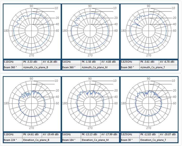
| Unit in dBi | XZ-plane Peak | XZ-plane Avg. | YZ-plane Peak | YZ-plane Avg. |
|---|---|---|---|---|
| @2400MHz | -3.59 | -7.32 | -13.15 | -22.67 |
| @2440MHz | -2.92 | -6.42 | -10.95 | -20.97 |
| @2480MHz | -3.1 | -6.54 | -11.15 | -20.92 |
| @5180MHz | -3.33 | -6.26 | -14.61 | -19.49 |
| @5600MHz | -1.58 | -4.88 | -13.13 | -17.99 |
| @5825MHz | -3.61 | -6.78 | -12.83 | -20.07 |
Antenna Radiation Patterns
2.4 GHz
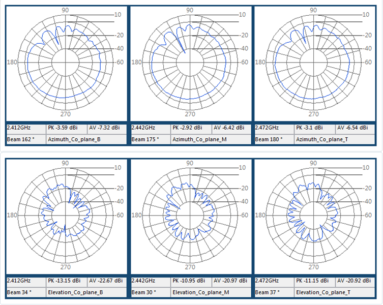
5 GHz
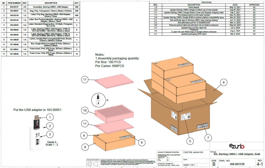
Shipping and Labeling
Packaging
450-00137 Single Unit
450-00137B Bulk
Environmental and Reliability
Reliability Tests
Climatic and Dynamic
| Test Item | Specification | Standard | Test Result |
|---|---|---|---|
| Vibration Non-Operating Unpackaged device | Vibration Wave Form: Sine Waveform Vibration frequency / Displacement: 20-80 Hz/1.5mm Vibration frequency / Acceleration: 80-2000 Hz/20g Cycle Time: 4 min/cycle Number of Cycles: 4 cycle/axis Vibration Axes: X, Y and Z (Rotate each axis on vertical vibration table) | JEDEC 22-B103B (2016) | Pass |
| Mechanical Shock Non-Operating Unpackaged device | Pulse shape: Half-sine waveform Impact acceleration: 1500 g Pulse duration: 0.5 ms Number of shocks: 30 shocks (5 shocks for each face) Orientation: Bottom, top, left, right, front, and rear faces | JEDEC 22-B110B.01 (2019) | Pass |
Reliability Prediction
| Ezurio Part Number | Environment | Standard | Test Result 30 ℃ (Hours) |
|---|---|---|---|
| 450-00137 450-00137B | Ground, Mobile, Uncontrolled | Telcordia SR-332 Issue 4. (2016) | 4,531,587.72 |
| Ezurio Part Number | Environment | Standard | Test Result 85 ℃ (Hours) |
|---|---|---|---|
| 450-00137 450-00137B | Ground, Mobile, Uncontrolled | Telcordia SR-332 Issue 4. (2016) | 292,581.92 |
Regulatory, Qualification & Certifications
Regulatory Approvals
Note: For complete regulatory information, refer to the Sterling LWB5+ Regulatory Information document which is also available from the Sterling LWB5+ product page.
The Sterling LWB5+ holds current certifications in the following countries:
| Country/Region | Regulatory ID |
|---|---|
| USA (FCC) | SQG-LWB5PLUS |
| EU | N/A |
| Canada (ISED) | 3147A-LWB5PLUS |
| Japan (MIC) | 201-200402 |
| Australia | N/A |
| New Zealand | N/A |
Federal Communication Commission Interference Statement
This equipment has been tested and found to comply with the limits for a Class B digital device, pursuant to Part 15 of the FCC Rules. These limits are designed to provide reasonable protection against harmful interference in a residential installation. This equipment generates, uses, and can radiate radio frequency energy and, if not installed and used in accordance with the instructions, may cause harmful interference to radio communications. However, there is no guarantee that interference will not occur in a particular installation. If this equipment does cause harmful interference to radio or television reception, which can be determined by turning the equipment off and on, the user is encouraged to try to correct the interference by one of the following measures:
- Reorient or relocate the receiving antenna.
- Increase the separation between the equipment and receiver.
- Connect the equipment into an outlet on a circuit different from that to which the receiver is connected.
- Consult the dealer or an experienced radio/TV technician for help.
FCC Caution: Any changes or modifications not expressly approved by the party responsible for compliance could void the user's authority to operate this equipment.
This device complies with Part 15 of the FCC Rules. Operation is subject to the following two conditions: (1) This device may not cause harmful interference, and (2) this device must accept any interference received, including interference that may cause undesired operation.
IMPORTANT NOTE:
Radiation Exposure Statement:
The product complies with the US portable RF exposure limit set forth for an uncontrolled environment and are safe for intended operation as described in this manual. The further RF exposure reduction can be achieved if the product can be kept as far as possible from the user body or set the device to lower output power if such function is available.
This transmitter must not be co-located or operating in conjunction with any other antenna or transmitter.
Industry Canada Statement
This device contains licence-exempt transmitter(s)/receiver(s) that comply with Innovation, Science and Economic Development Canada’s licence-exempt RSS(s). Operation is subject to the following two conditions:
(1) This device may not cause interference
(2) This device must accept any interference, including interference that may cause undesired operation of the device
L’émetteur/récepteur exempt de licence contenu dans le présent appareil est conforme aux CNR d’Innovation, Sciences et Développement économique Canada applicables aux appareils radio exempts de licence. L’exploitation est autorisée aux deux conditions suivantes :
(1) L’appareil ne doit pas produire de brouillage;
(2) L’appareil doit accepter tout brouillage radioélectrique subi, même si le brouillage est susceptible d’en compromettre le fonctionnement.
Radiation Exposure Statement:
The product complies with the Canada portable RF exposure limit set forth for an uncontrolled environment and are safe for intended operation as described in this manual. The further RF exposure reduction can be achieved if the product can be kept as far as possible from the user body or set the device to lower output power if such function is available.
Déclaration d'exposition aux radiations:
Le produit est conforme aux limites d'exposition pour les appareils portables RF pour les Etats-Unis et le Canada établies pour un environnement non contrôlé. Le produit est sûr pour un fonctionnement tel que décrit dans ce manuel. La réduction aux expositions RF peut être augmentée si l'appareil peut être conservé aussi loin que possible du corps de l'utilisateur ou que le dispositif est réglé sur la puissance de sortie la plus faible si une telle fonction est disponible.
Bluetooth SIG Qualification
The Bluetooth Qualification Process promotes global product interoperability and reinforces the strength of the Bluetooth® brand and ecosystem to the benefit of all Bluetooth SIG members. The Bluetooth Qualification Process helps member companies ensure their products that incorporate Bluetooth technology comply with the Bluetooth Patent & Copyright License Agreement and the Bluetooth Trademark License Agreement (collectively, the Bluetooth License Agreement) and Bluetooth Specifications.
The Bluetooth Qualification Process is defined by the Qualification Program Reference Document (QPRD) v3.
To demonstrate that a product complies with the Bluetooth Specification(s), each member must for each of its products:
- Identify the product, the design included in the product, the Bluetooth Specifications that the design implements, and the features of each implemented specification
- Complete the Bluetooth Qualification Process by submitting the required documentation for the product under a user account belonging to your company
The Bluetooth Qualification Process consists of the phases shown below:

To complete the Qualification Process the company developing a Bluetooth End Product shall be a member of the Bluetooth SIG. To start the application please use the following link: Apply for Adopter Membership
Scope
This guide is intended to provide guidance on the Bluetooth Qualification Process for End Products that reference multiple existing designs, that have not been modified, (refer to Section 3.2.2.1 of the Qualification Program Reference Document v3).
For a Product that includes a new Design created by combining two or more unmodified designs that have DNs or QDIDs into one of the permitted combinations in Table 3.1 of the QPRDv3, a Member must also provide the following information:
- DNs or QDIDs for Designs included in the new Design
- The desired Core Configuration of the new Design (if applicable, see Table 3.1 below)
- The active TCRL Package version used for checking the applicable Core Configuration (including transport compatibility) and evaluating test requirements
Any included Design must not implement any Layers using withdrawn specification(s).
When creating a new Design using Option 2a, the Inter-Layer Dependency (ILD) between Layers included in the Design will be checked based on the latest TCRL Package version used among the included Designs.
For the purposes of this document, it is assumed that the member is combining unmodified Core-Controller Configuration and Core-Host Configuration designs, to complete a Core-Complete Configuration.
Qualification Steps When Referencing multiple existing designs, (unmodified) – Option 2a in the QPRDv3
For this qualification option, follow these steps:
- To start a listing, go to: https://qualification.bluetooth.com/
- Select Start the Bluetooth Qualification Process.
Product Details to be entered:
- Project Name (this can be the product name or the Bluetooth Design name).
- Product Description
- Model Number
- Product Publication Date (the product publication date may not be later than 90 days after submission)
- Product Website (optional)
- Internal Visibility (this will define if the product will be visible to other users prior to publication)
- If you have multiple End Products to list then you can select ‘Import Multiple Products’, firstly downloading and completing the template, then by ‘Upload Product List’. This will populate Qualification Workspace with all your products.
Specify the Design:
- Do you include any existing Design(s) in your Product? Answer Yes, I do.
- Enter the multiple DNs or QDIDs used in your, (for Option 2a two or more DNs or QDIDs must be referenced)
- Select ‘I’m finished entering DN’s
- Once the DNs or QDIDs are selected they will appear on the left-hand side, indicating the layers covered by the design (should show Core-Controller and Core Host Layers covered).
- What do you want to do next? Answer, ‘Combine unmodified Designs’.
- The Qualification Workspace Tool will indicate that a new Design will be created and what type of Core-Complete configuration is selected.
- An active TCRL will be selected for the design.
- Perform the Consistency Check, which should result in no inconsistencies
- If there are any inconsistencies these will need to be resolved before proceeding
- Save and go to Test Plan and Documentation
Test Plan and Documentation
- As no modifications have been made to the combined designs the tool should report the following message:
‘No test plan has been generated for your new Design. Test declarations and test reports do not need to be submitted. You can continue to the next step.’ - Save and go to Product Qualification fee
- As no modifications have been made to the combined designs the tool should report the following message:
Product Qualification Fee:
- It’s important to make sure a Prepaid Product Qualification fee is available as it is required at this stage to complete the Qualification Process.
- Prepaid Product Qualification Fee’s will appear in the available list so select one for the listing.
- If one is not available select ‘Pay Product Qualification Fee’, payment can be done immediately via credit card, or you can pay via Invoice. Payment via credit will release the number immediately, if paying via invoice the number will not be released until the invoice is paid.
- Once you have selected the Prepaid Qualification Fee, select ‘Save and go to Submission’
Submission:
- Some automatic checks occur to ensure all submission requirements are complete.
- To complete the listing any errors must be corrected
- Once you have confirmed all design information is correct, tick all of the three check boxes and add your name to the signature page.
- Now select ‘Complete the Submission’.
- You will be asked a final time to confirm you want to proceed with the submission, select ‘Complete the Submission’.
- Qualification Workspace will confirm the submission has been submitted. The Bluetooth SIG will email confirmation once the submission has been accepted, (normally this takes 1 working day).
Download Product and Design Details (SDoC):
- You can now download a copy of the confirmed listing from the design listing page and save a copy in your Compliance Folder
For further information, please refer to the following webpage:
https://www.bluetooth.com/develop-with-bluetooth/qualification-listing/
Example Design Combinations
Ezurio Controller Subsystem + BlueZ 5.50 Host Stack (Ezurio Sterling LWB5+ based design)
| Design Name | Owner | Declaration ID | QD ID | Link to listing on the SIG website |
|---|---|---|---|---|
| Sterling LWB5+ | Ezurio | D050382 | 159315 | https://qualification.bluetooth.com/ListingDetails/119009 |
| BlueZ 5.50 Host Stack | Ezurio | D046330 | 138224 | https://qualification.bluetooth.com/ListingDetails/93911 |
Qualify More Products
If you develop further products based on the same design in the future, it is possible to add them free of charge. The new product must not modify the existing design i.e add ICS functionality, otherwise a new design listing will be required.
To add more products to your design, select ‘Manage Submitted Products’ in the Getting Started page, Actions, Qualify More Products. The tool will take you through the updating process.
Ordering Information
| Part Number | Description |
|---|---|
| 450-00137B | Sterling LWB5+, USB Adapter, Bulk |
Legacy - Revision History
| Version | Date | Notes | Contributors | Approver |
|---|---|---|---|---|
| 1.0 | 20 Aug 2021 | Initial version | Andrew Chen | Andy Ross |
| 1.1 | 30 May 2023 | Added support for latest WPA2/WPA3 Enterprise security standards | Dave Drogowski | Andy Ross |
| 1.2 | 3 Jan 2024 | Added 17 USB Adapter Integrated Antenna Performance | Andrew Chen | Andy Ross |
| 1.3 | 3 Apr 2024 | Added full support for WPA2/WPA3 Enterprise | Bob Monroe | Andy Ross |
| 1.4 | 22 May 2024 | Added Reliability Test section. Updated to Ezurio formatting. | Connie Lin | Andy Ross |
| 2.0 | 21 Oct 2024 | Ezurio rebranding. | Sue White | Andy Ross |
| 2.1 | 10 Mar 2025 | Update packaging from cardboard insert to EPE foam. | Connie Lin | Andy Ross |