/filters:background_color(white)/2024-03/Lyra%2024%20-%20Collection1.png)
Introduction
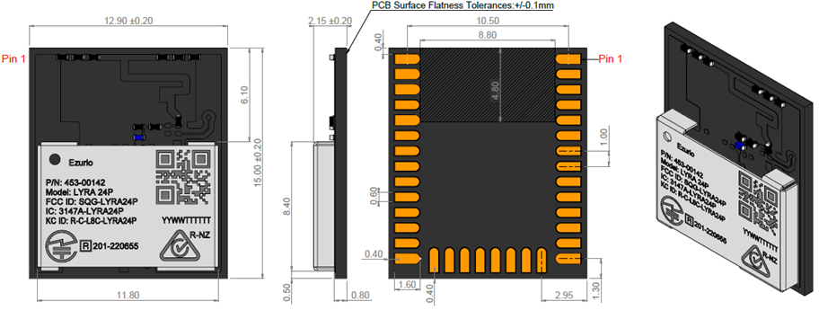
The Lyra 24P is a secure, high-performance wireless module optimized for the needs of battery and line powered IoT devices running on Bluetooth networks.
Based on the Series 2 EFR32BG24 SoC, it enables Bluetooth® Low Energy connectivity, delivering exceptional RF performance and energy efficiency, industry leading Secure Vault® technology, and future-proofing capabilities.
The Lyra 24P is a complete solution offered with robust and fully upgradeable software stacks, global regulatory certifications, advanced development and debugging tools, and documentation that simplifies and minimizes the development cycle of your end-product, helping to accelerate its time-to-market.
Overview
This document describes key hardware aspects of the Lyra 24P. This document is intended to assist device manufacturers and related parties with the integration of this radio into their host devices. Data in this document is drawn from several sources. For full documentation on the Lyra 24P, visit:
https://www.ezurio.com/lyra24-series
This datasheet is subject to change. Please contact Ezurio for further information.
Application Areas
- Smart Home Devices
- Lighting
- Building Automation and Security
- Gateways and Digital Assistants
- Bluetooth mesh Low Power Node
Features & Benefits
The Lyra 24P device features and benefits are described below.
- Bluetooth Low Energy 5.4
- Bluetooth Mesh connectivity
- Built-in antenna or RF pin
- +10 or +20 dBm TX output power (see 13.2, 13.3, and 13.5)
- -98.5 dBm BLE 1M RX sensitivity
- 32-bit ARM® Cortex®-M33 core at 39 MHz
- 1536/256 kB of Flash/RAM memory
- Vault High or Vault Mid security
- Rich set of analog and digital peripherals
- 26 GPIO pins
- -40 °C to 105 °C
- 12.9 mm x 15.0 mm
Specification Summary
Processor / SoC / Chipset
| Wireless | Silicon Labs Series 2 EFR32BG24 SoC
|
Bluetooth
| Standards | Bluetooth Low Energy (BLE) 5.4 Bluetooth Mesh |
| Receive Sensitivity |
|
| Peripheral Interface | 26x Multifunction I/O lines |
|---|---|
| UART | 1 × Universal Synchronous/Asynchronous Receiver/Transmitter (USART), supporting UART/SPI/SmartCard (ISO 7816)/IrDA/I2S 2 × Enhanced Universal Synchronous/Asynchronous Receiver/Transmitter (EUSART) supporting UART/SPI/DALI/ IrDA |
| GPIO | Up to 26 General Purpose I/O pins with output state retention and asynchronous interrupts |
| ADC |
|
| ACMP` | 2 × Analog Comparator (ACMP) |
| VDAC | 2 × Digital to Analog Converter (VDAC) |
| DMA | 8 Channel DMA Controller |
| PRS | 16 Channel Peripheral Reflex System (PRS) |
| Timers |
|
| I2C | 2 × I2C interface with SMBus support |
| TEMP | Die temperature sensor with +/- 1.5 °C accuracy after single-point calibration |
| Keypad Scanner | Keypad scanner supporting up to 6x8 matrix (KEYSCAN) |
| RF Oscillator | Low-Frequency RC Oscillator with precision mode to replace 32 kHz sleep crystal (LFRCO) |
Power
| Input Voltage |
|
| Current Consumption |
|
Mechanical
| Dimensions | 12.9 mm x 15.0 mm x 2.15 mm |
Software
| Security |
|
| Firmware | AT Command Set – fully featured and extensible to suit any developer’s needs.
C Code – Full software development with Silicon Labs SDK and Toolchain
|
Environmental
| Operating Temperature | -40 to +105°C |
| Lead Free | Lead-free and RoHS Compliant |
Certifications
| Regulatory Compliance |
|
Development
| Development Kit |
|
Warranty
| Warranty Terms | One Year Warranty |
Hardware Architecture
Block Diagrams
The Lyra 24P module is a highly integrated, high-performance system with all the hardware components needed to enable 2.4 GHz wireless connectivity and support robust networking capabilities via multiple wireless protocols.
Built around the EFR32BG24 Wireless SoC, the Lyra 24P includes a built-in antenna, an RF matching network (optimized for transmit power efficiency), supply decoupling and filtering components, an LC tank for DC-DC conversion, a 39 MHz reference crystal, and an RF shield. Also, it supports the use of an external 32 kHz crystal as a low frequency reference signal via GPIO pins for use cases demanding maximum energy efficiency.
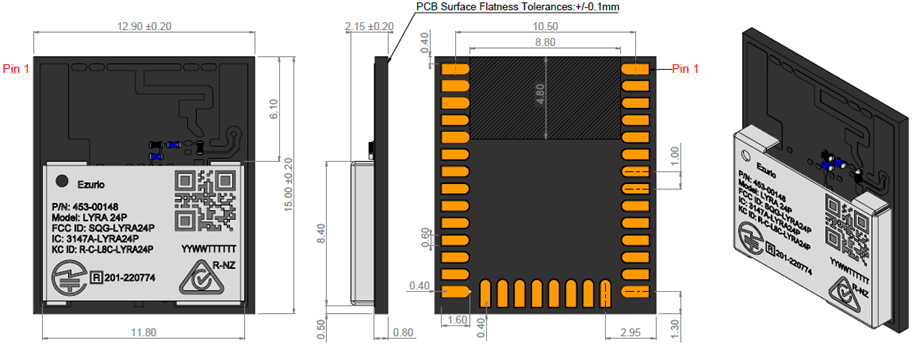
For designs where an external antenna solution may be beneficial, a module variant with a 50 Ω-matched RF pin instead of the built-in antenna is available (for Lyra 24P, RF, 20dBm, RF Trace only).
Because the RF matching network is optimized for transmit power efficiency, modules rated for +20 dBm will show non-optimal current consumption and performance when operated at a lower output power (i.e. +10 or 0 dBm).
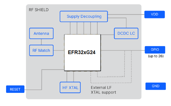
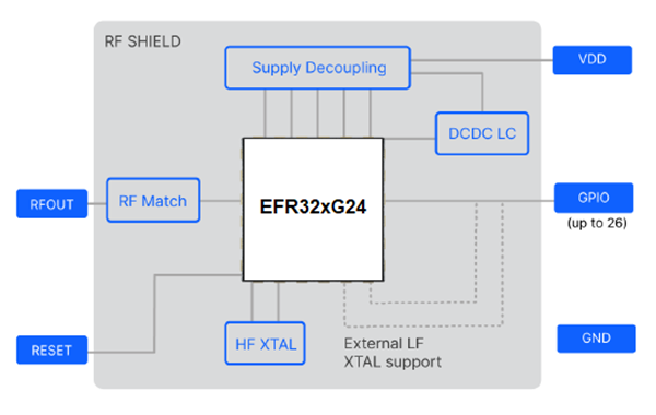
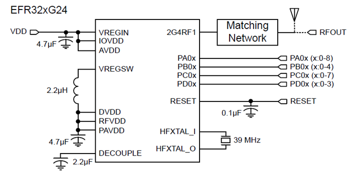
A simplified internal schematic for the Lyra 24P module is shown below.
EFR32BG24 SoC
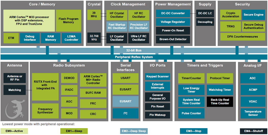
The EFR32BG24 SoC features a 32-bit ARM Cortex M33 core, a 2.4 GHz high-performance radio, 1536 kB of Flash memory, 256 kB of RAM, a dedicated core for security, a rich set of MCU peripherals, and various clock management and serial interfacing options. See the EFR32xG24 Reference Manual for details.
Integrated Antenna
Lyra 24P modules come with two antenna solutions variants: A built-in antenna or a 50 Ohms matched RF pin to support an external antenna. Typical performance characteristics of the built-in antenna are detailed in table below.
| Parameter | With Optimal Layout | Note |
|---|---|---|
| Efficiency | -1 dB | Antenna efficiency, gain, and radiation pattern are highly dependent on the application PCB layout and mechanical design. Refer toLayout on Host PCB for recommendations to achieve optimal antenna performance. |
| Peak gain | 1.82 dBi |
External Antenna
Lyra 24P module can be used with external antennas (certified by Ezurio) and requires a RF 50 Ohm track (Ground Coplanar Waveguide) to be designed to run from Lyra 24P module RFOUT (pin 33) to an RF antenna connector (IPEX MHF 4) on the host PCB. The 50 ohm RF track design and length MUST be copied as defined in section Lyra 24P 50 Ohms RF Track Design for Connecting External Antenna with the Lyra 24P Module, 20dBm, RF Pad Variant (453-00148).
The list of supported external antennas (certified by Ezurio) are listed in section External Antenna Integration with the Lyra 24P Module.
Power Supply
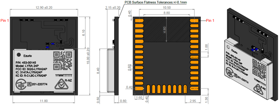
The Lyra 24P requires a single nominal supply level (VDD) to operate and supports an operating range of 1.8 to 3.8 V. The nominal level needed for +10 dBm devices (part number: 453-00142) is 3.0 V whereas +20 dBm devices (part number: 453-00145 and 453-00148) require 3.3 V in order to achieve higher TX output power. All necessary decoupling, filtering and DC-DC-related components are included in the module.
Note: The power amplifier for +10 dBm modules is supplied through an internal LDO, and thus is independent of the VDD supply. Respectively, the power amplifier for +20 dBm modules is supplied through the VDD pin with a target level of 3.3 V.
GPIO
The Lyra 24P has up to 26 General Purpose Input/Output pins. Each GPIO pin can be individually configured as either an output or input. More advanced configurations including open-drain, open-source, and glitch-filtering can be configured for each individual GPIO pin. The GPIO pins can be overridden by peripheral connections, like SPI communication. Each peripheral connection can be routed to several GPIO pins on the device. The input value of a GPIO pin can be routed through the Peripheral Reflex System to other peripherals. The GPIO subsystem supports asynchronous external pin interrupts.
All the pins on ports A and port B are EM2 capable. These pins may be used by Low-Energy peripherals in EM2/3 and may also be used as EM2/3 pin wake-ups. Pins on ports C and D are latched/retained in their current state when entering EM2 until EM2 exit upon which internal peripherals could once again drive those pads.
A few GPIOs also have EM4 wake functionality. These pins are listed in Alternate Pin Functions.
Security
Lyra 24P modules support one of two levels in the Security Portfolio offered by Silicon Labs: Secure Vault Mid or Secure Vault High. Lyra 24P modules support Secure Vault High.
Secure Vault is a collection of technologies that deliver state-of-the-art security and upgradability features to protect and future proof IoT devices against costly threats, attacks, and tampering. A dedicated security CPU enables the Secure Vault functions and isolates cryptographic functions and data from the Cortex-M33 core. Lyra 24P support Secure Vault High.
Secure Vault Features
| Feature | Secure Vault Mid | Secure Vault High |
|---|---|---|
| True Random Number Generator (TRNG) | Yes | Yes |
| Secure Boot with Root of Trust and Secure Loader (RTSL) | Yes | Yes |
| Secure Debug with Lock/Unlock | Yes | Yes |
| DPA Countermeasures | Yes | Yes |
| Anti-Tamper | Yes | |
| Secure Attestation | Yes | |
| Secure Key Management | Yes | |
| Symmetric Encryption |
|
|
| Public Key Encryption - ECDSA / ECDH / EdDSA |
|
|
| Key Derivation |
|
|
| Hashes |
|
|
Secure Boot with Root of Trust and Secure Loader (RTSL)
The Secure Boot with RTSL authenticates a chain of trusted firmware that begins from an immutable memory (ROM).
It prevents malware injection, prevents rollback, ensures that only authentic firmware is executed, and protects Over The Air updates. For more information about this feature, see Silicon Labs’ AN1218: Series 2 Secure Boot with RTSL.
Cryptographic Accelerator
The Cryptographic Accelerator is an autonomous hardware accelerator with Differential Power Analysis (DPA) countermeasures to protect keys.
It supports AES encryption and decryption with 128/192/256-bit keys, ChaCha20 encryption, and Elliptic Curve Cryptography (ECC) to support public key operations, and hashes.
Supported block cipher modes of operation for AES include:
- ECB (Electronic Code Book)
- CTR (Counter Mode)
- CBC (Cipher Block Chaining)
- CFB (Cipher Feedback)
- GCM (Galois Counter Mode)
- CCM (Counter with CBC-MAC)
- CBC-MAC (Cipher Block Chaining Message Authentication Code)
- GMAC (Galois Message Authentication Code)
The Cryptographic Accelerator accelerates Elliptical Curve Cryptography and supports the NIST (National Institute of Standards and Technology) recommended curves including P-192, P-256, P-384, and P-521 for ECDH (Elliptic Curve Diffie-Hellman) key derivation, and ECDSA (Elliptic Curve Digital Signature Algorithm) sign and verify operations. Also supported is the non-NIST Curve25519 for ECDH and Ed25519 for EdDSA (Edwards-curve Digital Signature Algorithm) sign and verify operations.
Secure Vault also supports ECJ-PAKE (Elliptic Curve variant of Password Authenticated Key Exchange by Juggling) and PBKDF2 (Password-Based Key Derivation Function 2).
Supported hashes include SHA-1, SHA-2/256/384/512 and Poly1305.
This implementation provides a fast and energy efficient solution to state of the art cryptographic needs.
True Random Number Generator
The True Random Number Generator module is a non-deterministic random number generator that harvests entropy from a thermal energy source. It includes start-up health tests for the entropy source as required by NIST SP800-90B and AIS-31 as well as online health tests required for NIST SP800-90C.
The TRNG is suitable for periodically generating entropy to seed an approved pseudo random number generator.
Secure Debug with Lock/Unlock
For obvious security reasons, it is critical for a product to have its debug interface locked before being released in the field.
In addition, Secure Vault High also provides a secure debug unlock function that allows authenticated access based on public key cryptography. This functionality is particularly useful for supporting failure analysis while maintaining confidentiality of IP and sensitive end-user data.
For more information about this feature, see Silicon Labs’ AN1190: Series 2 Secure Debug.
DPA Countermeasures
The AES and ECC accelerators have Differential Power Analysis (DPA) countermeasures support. This makes it very expensive from a time and effort standpoint to use DPA to recover secret keys.
Secure Key Management with PUF
Key material in Secure Vault High products is protected by "key wrapping" with a standardized symmetric encryption mechanism. This method has the advantage of protecting a virtually unlimited number of keys, limited only by the storage that is accessible by the Cortex-M33, which includes off-chip storage as well. The symmetric key used for this wrapping and unwrapping must be highly secure because it can expose all other key materials in the system. The Secure Vault Key Management system uses a Physically Unclonable Function (PUF) to generate a persistent device-unique seed key on power up to dynamically generate this critical wrapping/unwrapping key which is only visible to the AES encryption engine and is not retained when the device loses power.
Anti-Tamper
Secure Vault High devices provide internal tamper protection which monitors parameters such as voltage, temperature, and electro- magnetic pulses as well as detecting tamper of the security sub-system itself. Additionally, 8 external configurable tamper pins support external tamper sources, such as enclosure tamper switches.
For each tamper event, the user is able to select the severity of the tamper response ranging from an interrupt, to a reset, to destroying the PUF reconstruction data which will make all protected key materials un-recoverable and effectively render the device inoperable. The tamper system also has an internal resettable event counter with programmable trigger threshold and refresh periods to mitigate false positive tamper events.
For more information about this feature, see Silicon Labs’ AN1247: Anti-Tamper Protection Configuration and Use.
Secure Attestation
Secure Vault High products support Secure Attestation, which begins with a secure identity that is created during the Silicon Labs manufacturing process. During device production, each device generates its own public/private keypair and securely stores the wrapped private key into immutable OTP memory and this key never leaves the device. The corresponding public key is extracted from the device and inserted into a binary DER-encoded X.509 device certificate, which is signed into a Silicon Labs CA chain and then programmed back into the chip into an immutable OTP memory.
The secure identity can be used to authenticate the chip at any time in the life of the product. The production certification chain can be requested remotely from the product. This certification chain can be used to verify that the device was authentically produced by Silicon Labs. The device unique public key is also bound to the device certificate in the certification chain. A challenge can be sent to the chip at any point in time to be signed by the device private key. The public key in the device certificate can then be used to verify the challenge response, proving that the device has access to the securely stored private key, which prevents counterfeit products or impersonation attacks.
For more information about this feature, see Silicon Labs’ AN1268: Authenticating Silicon Labs Devices Using Device Certificates.
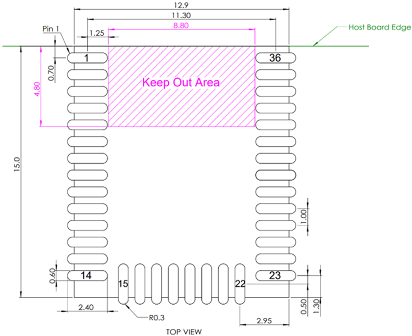
Pin-Out / Package Layout
Lyra 24P 36-Pin PCB Module Pinout
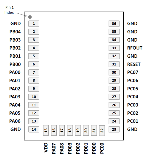
For GPIO pin to peripheral assignment in AT firmware, see User Guide – AT Interface Application – Lyra 24 Series.
The following table provides package pin connections and general descriptions of pin functionality. For detailed information on the supported features for each GPIO pin, see Alternate Pin Functions, Analog Peripheral Connectivity, and Digital Peripheral Connectivity.
| Pin Name | Pin(s) | Description | Pin Name | Pin(s) | Description |
|---|---|---|---|---|---|
| GND | 1 | Ground | PB04 | 2 | GPIO |
| PB03 | 3 | GPIO | PB02 | 4 | GPIO |
| PB01 | 5 | GPIO | PB00 | 6 | GPIO |
| PA00 | 7 | GPIO | PA01 | 8 | GPIO |
| PA02 | 9 | GPIO | PA03 | 10 | GPIO |
| PA04 | 11 | GPIO | PA05 | 12 | GPIO |
| PA06 | 13 | GPIO | GND | 14 | GND |
| VDD | 15 | Power Supply | PA07 | 16 | GPIO |
| PA08 | 17 | GPIO | PD03 | 18 | GPIO |
| PD02 | 19 | GPIO | PD01 | 20 | GPIO / LF XTAL Input (Optional) |
| PD00 | 21 | GPIO / LF XTAL Output (Optional) | PC00 | 22 | GPIO |
| GND | 23 | GPIO | PC01 | 24 | GPIO |
| PC02 | 25 | GPIO | PC03 | 26 | GPIO |
| PC04 | 27 | GPIO | PC05 | 28 | GPIO |
| PC06 | 29 | GPIO | PC07 | 30 | GPIO |
| RESETn | 31 | Reset Pin. The RESETn pin is pulled up to an internal DVDD supply. An external pull-up is not recommended. To apply an external reset source to this pin, it is required to only drive this pin low during reset, and let the internal pull-up ensure that reset is released. The RESETn pin can be left unconnected if no external reset switch or source is used. | GND | 32 | GND |
| RFOUT | 33 | RF Input/Output (External Ant.) | GND | 34 | GND |
| GND | 35 | GND | GND | 36 | GND |
Alternate Pin Functions
Some GPIOs support alternate functions like debugging, wake-up from EM4, external low frequency crystal access, etc.. The following table shows which module pins have alternate capabilities and the functions they support. Refer to the SoC's reference manual for more details.
| GPIO | Alternate Function | ||
|---|---|---|---|
| PA00 | IADC0.VREFP | ||
| PA01 | GPIO.SWCLK | ||
| PA02 | GPIO.SWDIO | ||
| PA03 | GPIO.SWV | GPIO.TDO | GPIO.TRACEDATA0 |
| PA04 | GPIO.TDI | GPIO.TRACECLK | |
| PA05 | GPIO.TRACEDATA1 | GPIO.EM4WU0 | |
| PA06 | GPIO.TRACEDATA2 | ||
| PA07 | GPIO.TRACEDATA3 | ||
| PB00 | VDAC0.VDAC_CH0_MAIN_OUTPUT | ||
| PB01 | GPIO.EM4WU3 | VDAC0.VDAC_CH_MAIN_OUTPUT | |
| PB02 | VDAC1.VDAC_CH0_MAIN_OUTPUT | ||
| PB03 | GPIO.EM4WU4 | VDAC1.VDAC_CH1_MAIN_OUTPUT | |
| PC00 | GPIO.EM4WU6 | ||
| PC01 | GPIO.EFP_TX_SDA | ||
| PC02 | GPIO.EFP_TX_SCL | ||
| PC05 | GPIO.EFP_INT | GPIO.EM4WU7 | |
| PC07 | GPIO.EM4WU8 | GPIO.THMSW_EN | GPIO.THMSW_HALFSWITCH |
| PD00 | LFXO.LFXTAL_O | ||
| PD01 | LFXO.LFXTAL_I | LFXO.LF_EXTCLK | |
| PD02 | GPIO.EM4WU9 | ||
Analog Peripheral Connectivity
Many analog resources are routable and can be connected to numerous GPIO's. The table below indicates which peripherals are available on each GPIO port. When a differential connection is being used, positive inputs are restricted to the EVEN pins and Negative inputs are restricted to the ODD pins. When a single ended connection is being used positive input is available on all pins. See the SoC’s Reference Manual for more details on the ABUS and analog peripherals, EFR32BG24 SoC.
| Peripheral | Signal | PA | PB | PC | PD | ||||
|---|---|---|---|---|---|---|---|---|---|
| EVEN | ODD | EVEN | ODD | EVEN | ODD | EVEN | ODD | ||
| ACMP0 | ana_neg | Yes | Yes | Yes | Yes | Yes | Yes | Yes | Yes |
| ana_pos | Yes | Yes | Yes | Yes | Yes | Yes | Yes | Yes | |
| ACMP1 | ana_neg | Yes | Yes | Yes | Yes | Yes | Yes | Yes | Yes |
| ana_pos | Yes | Yes | Yes | Yes | Yes | Yes | Yes | Yes | |
| IADC0 | ana_neg | Yes | Yes | Yes | Yes | Yes | Yes | Yes | Yes |
| ana_pos | Yes | Yes | Yes | Yes | Yes | Yes | Yes | Yes | |
| VDAC0 | VDAC_CH0_ABUS_OUTPUT | Yes | Yes | Yes | Yes | Yes | Yes | Yes | Yes |
| VDAC_CH1_ABUS_OUTPUT | Yes | Yes | Yes | Yes | Yes | Yes | Yes | Yes | |
| VDAC1 | VDAC_CH0_ABUS_OUTPUT | Yes | Yes | Yes | Yes | Yes | Yes | Yes | Yes |
| VDAC_CH1_ABUS_OUTPUT | Yes | Yes | Yes | Yes | Yes | Yes | Yes | Yes | |
Digital Peripheral Connectivity
Many digital resources are routable and can be connected to numerous GPIO's. The table below indicates which peripherals are available on each GPIO port.
| Peripheral.Resource | PORT | |||
|---|---|---|---|---|
| PA | PB | PC | PD | |
| ACMP0.DIGOUT | Available | Available | Available | Available |
| ACMP1.DIGOUT | Available | Available | ||
| CMU.CLKIN0 | Available | Available | ||
| CMU.CLKOUT0 | Available | Available | ||
| CMU.CLKOUT1 | Available | Available | ||
| CMU.CLKOUT2 | Available | Available | ||
| EUSART0.CS | Available | Available | ||
| EUSART0.CTS | Available | Available | ||
| EUSART0.RTS | Available | Available | ||
| EUSART0.RX | Available | Available | ||
| EUSART0.SCLK | Available | Available | ||
| EUSART0.TX | Available | Available | Available | Available |
| EUSART1.CS | Available | Available | Available | Available |
| EUSART1.CTS | Available | Available | Available | Available |
| EUSART1.RTS | Available | Available | Available | Available |
| EUSART1.RX | Available | Available | Available | Available |
| EUSART1.SCLK | Available | Available | Available | Available |
| EUSART1.TX | Available | Available | ||
| FRC.DCLK | Available | Available | ||
| FRC.DFRAME | Available | Available | ||
| FRC.DOUT | Available | Available | ||
| HFXO0.BUFOUT_REQ_IN_ASYNC | Available | Available | Available | Available |
| I2C0.SCL | Available | Available | Available | Available |
| I2C0.SDA | Available | Available | ||
| I2C1.SCL | Available | Available | ||
| I2C1.SDA | Available | Available | Available | Available |
| KEYSCAN.COL_OUT_0 | Available | Available | Available | Available |
| KEYSCAN.COL_OUT_1 | Available | Available | Available | Available |
| KEYSCAN.COL_OUT_2 | Available | Available | Available | Available |
| KEYSCAN.COL_OUT_3 | Available | Available | Available | Available |
| KEYSCAN.COL_OUT_4 | ||||
| KEYSCAN.COL_OUT_5 | Available | Available | Available | Available |
| KEYSCAN.COL_OUT_6 | Available | Available | Available | Available |
| KEYSCAN.COL_OUT_7 | Available | Available | Available | Available |
| KEYSCAN.ROW_SENSE_0 | Available | Available | ||
| KEYSCAN.ROW_SENSE_1 | Available | Available | ||
| KEYSCAN.ROW_SENSE_2 | Available | Available | ||
| KEYSCAN.ROW_SENSE_3 | Available | Available | ||
| KEYSCAN.ROW_SENSE_4 | Available | Available | ||
| KEYSCAN.ROW_SENSE_5 | Available | Available | ||
| LETIMER0.OUT0 | Available | Available | ||
| LETIMER0.OUT1 | Available | Available | ||
| MODEM.ANT0 | Available | Available | Available | Available |
| MODEM.ANT1 | Available | Available | Available | Available |
| MODEM.ANT_ROLL_OVER | Available | Available | ||
| MODEM.ANT_RR0 | Available | Available | ||
| MODEM.ANT_RR1 | Available | Available | ||
| MODEM.ANT_RR2 | Available | Available | ||
| MODEM.ANT_RR3 | Available | Available | ||
| MODEM.ANT_RR4 | Available | Available | ||
| MODEM.ANT_RR5 | Available | Available | ||
| MODEM.ANT_SW_EN | Available | Available | ||
| MODEM.ANT_SW_US | Available | Available | ||
| MODEM.ANT_TRIG | Available | Available | ||
| MODEM.ANT_TRIG_STOP | Available | Available | ||
| MODEM.DCLK | Available | Available | ||
| MODEM.DIN | Available | Available | ||
| MODEM.DOUT | Available | Available | ||
| PCNT0.S0IN | Available | Available | ||
| PCNT0.S1IN | Available | Available | ||
| PRS.ASYNCH0 | Available | Available | ||
| PRS.ASYNCH1 | Available | Available | ||
| PRS.ASYNCH2 | Available | Available | ||
| PRS.ASYNCH3 | Available | Available | ||
| PRS.ASYNCH4 | Available | Available | ||
| PRS.ASYNCH5 | Available | Available | ||
| PRS.ASYNCH6 | Available | Available | ||
| PRS.ASYNCH7 | Available | Available | ||
| PRS.ASYNCH8 | Available | Available | ||
| PRS.ASYNCH9 | Available | Available | ||
| PRS.ASYNCH10 | Available | Available | ||
| PRS.ASYNCH11 | Available | Available | ||
| PRS.ASYNCH12 | Available | Available | ||
| PRS.ASYNCH13 | Available | Available | ||
| PRS.ASYNCH14 | Available | Available | ||
| PRS.ASYNCH15 | Available | Available | ||
| PRS.SYNCH0 | Available | Available | Available | Available |
| PRS.SYNCH1 | Available | Available | Available | Available |
| PRS.SYNCH2 | Available | Available | Available | Available |
| PRS.SYNCH3 | Available | Available | Available | Available |
| RAC.LNAEN | Available | Available | Available | Available |
| RAC.PAEN | Available | Available | Available | Available |
| TIMER0.CC0 | Available | Available | Available | Available |
| TIMER0.CC1 | Available | Available | Available | Available |
| TIMER0.CC2 | Available | Available | Available | Available |
| TIMER0.CDTI0 | Available | Available | Available | Available |
| TIMER0.CDTI1 | Available | Available | Available | Available |
| TIMER0.CDTI2 | Available | Available | Available | Available |
| TIMER1.CC0 | Available | Available | Available | Available |
| TIMER1.CC1 | Available | Available | Available | Available |
| TIMER1.CC2 | Available | Available | Available | Available |
| TIMER1.CDTI0 | Available | Available | Available | Available |
| TIMER1.CDTI1 | Available | Available | Available | Available |
| TIMER1.CDTI2 | Available | Available | Available | Available |
| TIMER2.CC0 | Available | Available | ||
| TIMER2.CC1 | Available | Available | ||
| TIMER2.CC2 | Available | Available | ||
| TIMER2.CDTI0 | Available | Available | ||
| TIMER2.CDTI1 | Available | Available | ||
| TIMER2.CDTI2 | Available | Available | ||
| TIMER3.CC0 | Available | Available | ||
| TIMER3.CC1 | Available | Available | ||
| TIMER3.CC2 | Available | Available | ||
| TIMER3.CDTI0 | Available | Available | ||
| TIMER3.CDTI1 | Available | Available | ||
| TIMER3.CDTI2 | Available | Available | ||
| TIMER4.CC0 | Available | Available | ||
| TIMER4.CC1 | Available | Available | ||
| TIMER4.CC2 | Available | Available | ||
| TIMER4.CDTI0 | Available | Available | ||
| TIMER4.CDTI1 | Available | Available | ||
| TIMER4.CDTI2 | Available | Available | ||
| USART0.CLK | Available | Available | Available | Available |
| USART0.CS | Available | Available | Available | Available |
| USART0.CTS | Available | Available | Available | Available |
| USART0.RTS | Available | Available | Available | Available |
| USART0.RX | Available | Available | Available | Available |
| USART0.TX | Available | Available | Available | Available |
Mechanical Drawings
Electrical Characteristics
All electrical parameters in all tables are specified under the following conditions, unless stated otherwise:
- Typical values are based on TA=25 °C and VDD supply at 3.0 V, by production test and/or technology characterization.
- Radio performance numbers are measured in conducted mode, based on Silicon Laboratories reference designs using output power-specific external RF impedance-matching networks for interfacing to a 50 Ω antenna.
- Minimum and maximum values represent the worst conditions across supply voltage, process variation, and operating temperature, unless stated otherwise.
Absolute Maximum Ratings
| Parameter | Symbol | Test Condition | Min | Typ | Max | Unit |
|---|---|---|---|---|---|---|
| Storage temperature range | TSTG | -40 | — | +105 | °C | |
| Voltage on VDD supply pin | VDDMAX | -0.3 | — | 3.8 | V | |
| Voltage ramp rate on VDD supply pin | VDDRAMPMAX | — | — | 1.0 | V/µs | |
| DC voltage on any GPIO pin | VDIGPIN | -0.3 | — | VVDD+0.3 | V | |
| DC voltage on RESETn pin1 | VRESETn | -0.3 | — | 3.8 | V | |
| Absolute voltage on RFOUT pin | VMAX2G4 | -0.3 | — | VVDD+0.3 | V | |
| Total current into VDD pin | IVDDMAX | Source | — | — | 200 | mA |
| Total current into GND pin | IGNDMAX | Sink | — | — | 200 | mA |
| Current per I/O pin | IIOMAX | Sink | — | — | 50 | mA |
| Source | — | — | 50 | mA | ||
| Current for all I/O pins | IIOALLMAX | Sink | — | — | 200 | mA |
| Source | — | — | 200 | mA |
Notes:
- The RESETn pin has a pull-up device to the internal DVDD supply. For minimum leakage, RESETn should not exceed the voltage at DVDD, which is generated by the DC-DC converter. DVDD is equal to 1.8 V when DC-DC is active and bypassed to VDD when DC-DC is inactive.
Recommended Operating Conditions
| Parameter | Symbol | Test Condition | Min | Typ | Max | Unit |
|---|---|---|---|---|---|---|
| Operating ambient temperature range | TA | -40 | — | +105 | °C | |
| VDD operating supply voltage | VVDD | 10 dBm Module, DC-DC in regulation | 2.2 | 3.0 | 3.8 | V |
| 20 dBm Module, DC-DC in regulation | 2.2 | 3.3 | 3.8 | V | ||
| 10 dBm Module, DC-DC in bypass | 1.8 | 3.0 | 3.8 | V | ||
| 20 dBm Module, DC-DC in bypass | 1.8 | 3.3 | 3.8 | V | ||
| HCLK and SYSCLK frequency | fHCLK | VSCALE2, MODE = WS1 | — | — | 78 | MHz |
| VSCALE2, MODE = WS0 | — | — | 40 | MHz | ||
| PCLK frequency | fPCLK | VSCALE2 or VSCALE1 | — | — | 40 | MHz |
| EM01 Group A clock frequency | fEM01GRPACLK | VSCALE2 | — | — | 78 | MHz |
| VSCALE1 | — | — | 40 | MHz | ||
| EM01 Group C clock frequency | fEM01GRPBCLK | VSCALE2 | — | — | 78 | MHz |
| VSCALE1 | — | — | 40 | MHz | ||
| Radio HCLK frequency | fRHCLK | VSCALE2 or VSCALE1 | — | 39.0 | — | MHz |
Current Consumption
MCU Current Consumption with 3 V Supply
Unless otherwise indicated, typical conditions are: VDD = 3.0 V, DC-DC in regulation. Voltage scaling level = VSCALE1. TA = 25 °C. Minimum and maximum values in this table represent the worst conditions across process variation at TA = 25 °C.
| Parameter | Symbol | Test Condition | Min | Typ | Max | Unit |
|---|---|---|---|---|---|---|
| Current consumption in EM0 mode with all peripherals disabled | IACTIVE | 78 MHz HFRCO w/ DPLL referenced to 39 MHz crystal, CPU running Prime from flash, VSCALE2 | — | 33.3 | — | µA/MHz |
| 78 MHz HFRCO w/ DPLL referenced to 39 MHz crystal, CPU running while loop from flash, VSCALE2 | — | 32.8 | — | µA/MHz | ||
| 78 MHz HFRCO w/ DPLL referenced to 39 MHz crystal, CPU running CoreMark loop from flash, VSCALE2 | — | 49.1 | — | µA/MHz | ||
| 39 MHz crystal, CPU running Prime from flash | — | 33.9 | — | µA/MHz | ||
| 39 MHz crystal, CPU running while loop from flash | — | 33.4 | — | µA/MHz | ||
| 39 MHz crystal, CPU running CoreMark loop from flash | — | 49.4 | — | µA/MHz | ||
| 38 MHz HFRCO, CPU running while loop from flash | — | 28.1 | — | µA/MHz | ||
| Current consumption in EM1 mode with all peripherals disabled | IEM1 | 78 MHz HFRCO w/ DPLL referenced to 39 MHz crystal, VSCALE2 | — | 22.6 | — | µA/MHz |
| 39 MHz crystal | — | 24.4 | — | µA/MHz | ||
| 38 MHz HFRCO | — | 19.0 | — | µA/MHz | ||
| Current consumption in EM2 mode, VSCALE0 | IEM2_VS | 256 kB RAM and full Radio RAM retention, RTC running from LFXO1 | — | 2.9 | — | µA |
| 256 kB RAM and full Radio RAM retention, RTC running from LFRCO1 | — | 2.9 | — | µA | ||
| 16 kB RAM and full Radio RAM retention, RTC running from LFXO1 | — | 1.3 | — | µA | ||
| 16 kB RAM and full Radio RAM retention, RTC running from LFRCO1 | — | 1.3 | — | µA | ||
| 16 kB RAM and full Radio RAM retention, RTC running from LFRCO in precision mode1 | — | 1.9 | — | µA | ||
| Current consumption in EM3 mode, VSCALE0 | IEM3_VS | 256 kB RAM and full Radio RAM retention, RTC running from ULFRCO1 | — | 2.7 | — | µA |
| 16 kB RAM and full Radio RAM retention, RTC running from ULFRCO1 | — | 1.1 | — | µA | ||
| Current consumption in EM4 mode | IEM4 | No BURTC, No LF Oscillator | — | 0.27 | — | µA |
| BURTC with LXO | — | 0.64 | — | µA | ||
| Current consumption during reset | IRST | Hard pin reset held | — | 467 | — | µA |
Notes:
- CPU cache retained, EM0/EM1 peripheral states retained.
Radio Current Consumption with 3 V Supply
RF current consumption measured with MCU in EM1 and all MCU peripherals disabled. Unless otherwise indicated, typical conditions are: VDD = 3.0 V, DC-DC in regulation. TA = 25 °C.
| Parameter | Symbol | Test Condition | Min | Typ | Max | Unit |
|---|---|---|---|---|---|---|
| Current consumption in receive mode, active packet reception, VSCALE1, EM1P | IRX_ACTIVE | 125 kbit/s, 2GFSK, f = 2.4 GHz | — | 4.8 | — | mA |
| 500 kbit/s, 2GFSK, f = 2.4 GHz | — | 4.9 | — | mA | ||
| 1 Mbit/s, 2GFSK, f = 2.4 GHz | — | 4.5 | — | mA | ||
| 2 Mbit/s, 2GFSK, f = 2.4 GHz | — | 5.2 | — | mA | ||
Current consumption in receive mode, listening for packet, VSCALE1, EM1P | IRX_LISTEN | 125 kbit/s, 2GFSK, f = 2.4 GHz | — | 4.8 | — | mA |
| 500 kbit/s, 2GFSK, f = 2.4 GHz | — | 4.8 | — | mA | ||
| 1 Mbit/s, 2GFSK, f = 2.4 GHz | — | 4.5 | — | mA | ||
| 2 Mbit/s, 2GFSK, f = 2.4 GHz | — | 5.2 | — | mA | ||
Current consumption in transmit mode | ITX | f = 2.4 GHz, CW, 0 dBm output power | — | 4.8 | — | mA |
| f = 2.4 GHz, CW, +10 dBm output power | — | 18.8 | — | mA | ||
| f = 2.4 GHz, CW, +20 dBm output power, VDD = 3.3 V1 | — | 154.8 | — | mA |
Notes:
- Maximum output power for Bluetooth Low Energy is limited to 19.6 dBm for compliance with the Bluetooth Core Specifications.
DC Electrical Characteristics
RF Transmitter General Characteristics for the 2.4 GHz Band
Unless otherwise indicated, typical conditions are: VDD = 3.0 V, DC-DC in regulation. RF center frequency 2.45 GHz. TA=25°C.
| Parameter | Symbol | Test Condition (Output Power) | Min | Typ | Max | Unit |
|---|---|---|---|---|---|---|
| RF tuning frequency range | FRANGE | 2402 | — | 2480 | MHz | |
| Maximum TX power | POUTMAX | 0 dBm | — | -0.3 | — | dBm |
| +10 dBm | — | 10 | — | dBm | ||
| +20 dBm, VDD = 3.3 V1 | — | 19.6 | — | dBm | ||
| Minimum active TX Power | POUTMIN | 0 dBm | — | -24 | — | dBm |
| +10 dBm | — | -30 | — | dBm | ||
| +20 dBm, VDD = 3.3 V | — | -33.7 | — | dBm | ||
| Output power step size | POUTSTEP | 0 dBm | 0.1 | 0.7 | 9.9 | dBm |
| +10 dBm, -5 dBm < Output power < 0 dBm | 0.6 | 1.1 | 1.8 | dBm | ||
| +10 dBm, 0 dBm < Output power < 10 dBm | 0.1 | 0.3 | 0.8 | dBm | ||
| +20 dBm, VDD = 3.3 V, Output power < 0 dBm | 0.9 | 3.6 | 14.4 | dBm | ||
| +20 dBm, 0 dBm < Output power < 20 dBm | 0.1 | 0.2 | 1.3 | dBm | ||
| Output power variation vs VDD supply voltage variation, frequency = 2450 MHz | POUTVAR_V | 0 dBm with VDD voltage swept from 1.8 V to 3.8 V | — | 0.01 | — | dB |
| +10 dBm with VDD voltage swept from 1.8 V to 3.8 V | — | 0.05 | — | dB | ||
| +20 dBm with VDD voltage swept from 1.8 V to 3.8 V | — | 5.4 | — | dB | ||
| Output power variation vs temperature, Frequency = 2450 MHz | POUTVAR_T | 0 dBm, (-40 to +105 °C) | — | 1.0 | — | dB |
| +10 dBm, (-40 to +105 °C) | — | 0.3 | — | dB | ||
| +20 dBm, VDD = 3.3 V, (-40 to +105 °C) | — | 0.2 | — | dB | ||
| Output power variation vs RF frequency | POUTVAR_F | 0 dBm | — | 0.2 | — | dB |
| +10 dBm | — | 0.2 | — | dB | ||
| +20 dBm, VDD = 3.3 V | — | 0.2 | — | dB |
Notes:
- Maximum output power for Bluetooth Low Energy is limited to 19.6 dBm for compliance with the Bluetooth Core Specifications.
RF Receiver General Characteristics for the 2.4 GHz Band
Unless otherwise indicated, typical conditions are: VDD = 3.0 V, DC-DC in regulation. RF center frequency 2.45 GHz. TA = 25°C.
| Parameter | Symbol | Test Condition | Min | Typ | Max | Unit |
|---|---|---|---|---|---|---|
| RF tuning frequency range | FRANGE | 2402 | — | 2480 | MHz |
Unless otherwise indicated, typical conditions are: VDD = 3.0 V, DC-DC in regulation. RF center frequency 2.45 GHz. TA = 25 °C.
| Parameter | Symbol | Test Condition | Min | Typ | Max | Unit |
|---|---|---|---|---|---|---|
| Max usable receiver input level | SAT | Signal is reference signal1 | — | 10 | — | dBm |
| Sensitivity | SENS | +10 dBm Module, Signal is reference signal, 37 byte payload1 | — | -98.5 | — | dBm |
| +10 dBm Module, Signal is reference signal, 255 byte payload1 | — | -96.9 | — | dBm | ||
| +10 dBm Module, With non-ideal signals2 1 | — | -96.5 | — | dBm | ||
| +20 dBm Module, Signal is reference signal, 37 byte payload1 | — | -97.6 | — | dBm | ||
| +20 dBm Module, Signal is reference signal, 255 byte payload1 | — | -96 | — | dBm | ||
| +20 dBm Module, With non-ideal signals2 1 | — | -95.6 | — | dBm | ||
| Signal to co-channel interferer | C/ICC | (see notes)1 3 | — | 8.7 | — | dB |
| N ± 1 Adjacent channel selectivity | C/I1 | Interferer is reference signal at +1 MHz offset1 3 4 5 | — | -5.4 | — | dB |
| Interferer is reference signal at -1 MHz offset1 3 4 5 | — | -5.3 | — | dB | ||
| N ± 2 Alternate channel selectivity | C/I2 | Interferer is reference signal at +2 MHz offset1 3 4 5 | — | -40.9 | — | dB |
| Interferer is reference signal at -2 MHz offset1 3 4 5 | — | -39.7 | — | dB | ||
| N ± 3 Alternate channel selectivity | C/I3 | Interferer is reference signal at +3 MHz offset1 3 4 5 | — | -45.5 | — | dB |
| Interferer is reference signal at -3 MHz offset1 3 4 5 | — | -45.7 | — | dB | ||
| Selectivity to image frequency | C/IIM | Interferer is reference signal at image frequency with 1 MHz precision1 5 | — | -23.3 | — | dB |
| Selectivity to image frequency ± 1 MHz | C/IIM_1 | Interferer is reference signal at image frequency +1 MHz with 1 MHz precision1 5 | — | -40.9 | — | dB |
| Interferer is reference signal at image frequency -1 MHz with 1 MHz precision1 5 | — | -5.4 | — | dB | ||
| Intermodulation performance | IM | n = 3 (see note6) | — | -17.3 | — | dBm |
Notes:
- 0.017% Bit Error Rate.
- With non-ideal signals as specified in Bluetooth Test Specification RF-PHY.TS.5.0.1 section 4.7.1
- Desired signal -67 dBm.
- Desired frequency 2402 MHz ≤ Fc ≤ 2480 MHz.
- With allowed exceptions.
- As specified in Bluetooth Core specification version 5.1, Vol 6, Part A, Section 4.4
RF Receiver Characteristics for Bluetooth Low Energy in the 2.4 GHz Band 2 Mbps Data Rate
Unless otherwise indicated, typical conditions are: VDD = 3.0 V, DC-DC in regulation. RF center frequency 2.45 GHz. TA = 25 °C.
| Parameter | Symbol | Test Condition | Min | Typ | Max | Unit |
|---|---|---|---|---|---|---|
| Max usable receiver input level | SAT | Signal is reference signal1 | — | 10 | — | dBm |
| Sensitivity | SENS | +10 dBm Module, Signal is reference signal, 37 byte payload1 | — | -95.7 | — | dBm |
| +10 dBm Module, Signal is reference signal, 255 byte payload1 | — | -94.2 | — | dBm | ||
| +10 dBm Module, With non-ideal signals2 1 | — | -93.9 | — | dBm | ||
| +20 dBm Module, Signal is reference signal, 37 byte payload1 | — | -94.8 | — | dBm | ||
| +20 dBm Module, Signal is reference signal, 255 byte payload1 | — | -93.3 | — | dBm | ||
| +20 dBm Module, With non-ideal signals2 1 | — | -93.1 | — | dBm | ||
| Signal to co-channel interferer | C/ICC | (see notes)1 3 | — | 8.6 | — | dB |
| N ± 1 Adjacent channel selectivity | C/I1 | Interferer is reference signal at +2 MHz offset1 5 4 3 | — | -5.3 | — | dB |
| Interferer is reference signal at -2 MHz offset1 5 4 3 | — | -5.8 | — | dB | ||
| N ± 2 Alternate channel selectivity | C/I2 | Interferer is reference signal at +4 MHz offset1 5 4 3 | — | -42.2 | — | dB |
| Interferer is reference signal at -4 MHz offset1 5 4 3 | — | -44.2 | — | dB | ||
| N ± 3 Alternate channel selectivity | C/I3 | Interferer is reference signal at +6 MHz offset1 5 4 3 | — | -48.1 | — | dB |
| Interferer is reference signal at -6 MHz offset1 5 4 3 | — | -50.2 | — | dB | ||
| Selectivity to image frequency | C/IIM | Interferer is reference signal at image frequency with 1 MHz precision1 5 | — | -22.8 | — | dB |
| Selectivity to image frequency ± 2 MHz | C/IIM_1 | Interferer is reference signal at image frequency +2 MHz with 1 MHz precision1 5 | — | -42.2 | — | dB |
| Interferer is reference signal at image frequency -2 MHz with 1 MHz precision1 5 | — | -5.3 | — | dB | ||
| Intermodulation performance | IM | n = 3 (see note6) | — | -18.3 | — | dBm |
Notes:
- 0.017% Bit Error Rate.
- With non-ideal signals as specified in Bluetooth Test Specification RF-PHY.TS.5.0.1 section 4.7.1
- Desired signal -64 dBm.
- Desired frequency 2402 MHz ≤ Fc ≤ 2480 MHz.
- With allowed exceptions.
- As specified in Bluetooth Core specification version 5.1, Vol 6, Part A, Section 4.4
RF Receiver Characteristics for Bluetooth Low Energy in the 2.4 GHz Band 500 kbps Data Rate
Unless otherwise indicated, typical conditions are: VDD = 3.0 V, DC-DC in regulation. RF center frequency 2.45 GHz. TA = 25 °C.
| Parameter | Symbol | Test Condition | Min | Typ | Max | Unit |
|---|---|---|---|---|---|---|
| Max usable receiver input level | SAT | Signal is reference signal1 | — | 10 | — | dBm |
| Sensitivity | SENS | +10 dBm Module, Signal is reference signal, 37-byte payload1 | — | -102.2 | — | dBm |
| +10 dBm Module, Signal is reference signal, 255-byte payload1 | — | -101 | — | dBm | ||
| +10 dBm Module, With non-ideal signals2 1 | — | -100 | — | dBm | ||
| +20 dBm Module, Signal is reference signal, 37-byte payload1 | — | -101.4 | — | dBm | ||
| +20 dBm Module, Signal is reference signal, 255-byte payload1 | — | -100 | — | dBm | ||
| +20 dBm Module, With non-ideal signals2 1 | — | -99 | — | dBm | ||
| Signal to co-channel interferer | C/ICC | (see notes)1 3 | — | 2.7 | — | dB |
| N ± 1 Adjacent channel selectivity | C/I1 | Interferer is reference signal at +1 MHz offset1 3 4 5 | — | -7.1 | — | dB |
| Interferer is reference signal at -1 MHz offset1 3 4 5 | — | -7.4 | — | dB | ||
| N ± 2 Alternate channel selectivity | C/I2 | Interferer is reference signal at +2 MHz offset1 3 4 5 | — | -46.8 | — | dB |
| Interferer is reference signal at -2 MHz offset1 3 4 5 | — | -49.7 | — | dB | ||
| N ± 3 Alternate channel selectivity | C/I3 | Interferer is reference signal at +3 MHz offset1 3 4 5 | — | -49.4 | — | dB |
| Interferer is reference signal at -3 MHz offset1 3 4 5 | — | -54.5 | — | dB | ||
| Selectivity to image frequency | C/IIM | Interferer is reference signal at image frequency with 1 MHz precision1 5 | — | -49 | — | dB |
| Selectivity to image frequency ± 1 MHz | C/IIM_1 | Interferer is reference signal at image frequency +1 MHz with 1 MHz precision1 5 | — | -49.4 | — | dB |
| Interferer is reference signal at image frequency -1 MHz with 1 MHz precision1 5 | — | -46.8 | — | dB |
Notes:
- 0.017% Bit Error Rate.
- With non-ideal signals as specified in Bluetooth Test Specification RF-PHY.TS.5.0.1 section 4.7.1
- Desired signal -72 dBm.
- Desired frequency 2402 MHz ≤ Fc ≤ 2480 MHz.
- With allowed exceptions.
RF Receiver Characteristics for Bluetooth Low Energy in the 2.4 GHz Band 125 kbps Data Rate
Unless otherwise indicated, typical conditions are: VDD = 3.0 V, DC-DC in regulation. RF center frequency 2.45 GHz. TA = 25 °C.
| Parameter | Symbol | Test Condition | Min | Typ | Max | Unit |
|---|---|---|---|---|---|---|
| Max usable receiver input level | SAT | Signal is reference signal1 | — | 10 | — | dBm |
| Sensitivity | SENS | +10 dBm Module, Signal is reference signal, 37 byte payload1 | — | -106.5 | — | dBm |
| +10 dBm Module, Signal is reference signal, 255 byte payload1 | — | -106.1 | — | dBm | ||
| +10 dBm Module, With non-ideal signals2 1 | — | -105.7 | — | dBm | ||
| +20 dBm Module, Signal is reference signal, 37 byte payload1 | — | -105.6 | — | dBm | ||
| +20 dBm Module, Signal is reference signal, 255 byte payload1 | — | -105.3 | — | dBm | ||
| +20 dBm Module, With non-ideal signals2 1 | — | -104.8 | — | dBm | ||
| Signal to co-channel interferer | C/ICC | (see notes)1 3 | — | 0.9 | — | dB |
| N ± 1 Adjacent channel selectivity | C/I1 | Interferer is reference signal at +1 MHz offset1 3 4 5 | — | -12.4 | — | dB |
| Interferer is reference signal at -1 MHz offset1 3 4 5 | — | -12.8 | — | dB | ||
| N ± 2 Alternate channel selectivity | C/I2 | Interferer is reference signal at +2 MHz offset1 3 4 5 | — | -52.6 | — | dB |
| Interferer is reference signal at -2 MHz offset1 3 4 5 | — | -55.5 | — | dB | ||
| N ± 3 Alternate channel selectivity | C/I3 | Interferer is reference signal at +3 MHz offset1 3 4 5 | — | -53.8 | — | dB |
| Interferer is reference signal at -3 MHz offset1 3 4 5 | — | -60.0 | — | dB | ||
| Selectivity to image frequency | C/IIM | Interferer is reference signal at image frequency with 1 MHz precision1 5 | — | -53.0 | — | dB |
| Selectivity to image frequency ± 1 MHz | C/IIM_1 | Interferer is reference signal at image frequency +1 MHz with 1 MHz precision1 5 | — | -53.8 | — | dB |
| Interferer is reference signal at image frequency -1 MHz with 1 MHz precision1 5 | — | -52.6 | — | dB |
Notes:
- 0.017% Bit Error Rate.
- With non-ideal signals as specified in Bluetooth Test Specification RF-PHY.TS.5.0.1 section 4.7.1
- Desired signal -79 dBm.
- Desired frequency 2402 MHz ≤ Fc ≤ 2480 MHz.
- With allowed exceptions.
High-Frequency Crystal
| Parameter | Symbol | Test Condition | Min | Typ | Max | Unit |
|---|---|---|---|---|---|---|
| Crystal frequency | fHFXTAL | — | 39 | — | MHz | |
| Initial calibrated accuracy | ACCHFXTAL | -10 | ±5 | 10 | ppm | |
| Temperature drift | DRIFTHFXTAL | Across specified temperature range | -20 | — | 20 | ppm |
Low-Frequency Crystal Oscillator
| Parameter | Symbol | Test Condition | Min | Typ | Max | Unit |
|---|---|---|---|---|---|---|
| Crystal frequency | fLFXO | — | 32.768 | — | kHz | |
| Supported Crystal equivalent series resistance (ESR) | ESRLFXO | GAIN = 0 | — | — | 80 | kOhms |
| GAIN = 1 to 3 | — | — | 100 | kOhms | ||
| Supported range of crystal load capacitance1 | CL_LFXO | GAIN = 0 | 4 | — | 6 | pF |
| GAIN = 1 | 6 | — | 10 | pF | ||
| GAIN = 2 (see note 2) | 10 | — | 12.5 | pF | ||
| GAIN = 3 (see note 2) | 12.5 | — | 18 | pF | ||
| Current consumption | ICL12p5 | ESR = 70 kΩ, CL = 12.5pF, GAIN3 = 2, AGC4 = 1 | — | 294 | — | nA |
| Startup Time | TSTARTUP | ESR = 70 kΩ, CL = 7pF, GAIN3 = 1, AGC4 = 1 | — | 52 | — | ms |
| On-chip tuning cap step size | SSLFXO | — | 0.26 | — | pF | |
| On-chip tuning capacitor value at minimum setting5 | CLFXO_MIN | CAPTUNE=0 | — | 5.2 | — | pF |
| On-chip tuning capacitor value at maximum setting5 | CLFXO_MAX | CAPTUNE=0x4F | — | 26.2 | — | pF |
Notes:
- Total load capacitance seen by the crystal
- Crystals with a load capacitance of greater than 12pF require external load capacitors.
- In LFXO_CAL Register
- In LFXO_CFG Register
- The effective load capacitance seen by the crystal will be CLFXO/2. This is because each XTAL pin has a tuning cap, and the two caps will be seen in series by the crystal
Precision Low Frequency RC Oscillator (LFRCO)
| Parameter | Symbol | Test Condition | Min | Typ | Max | Unit |
|---|---|---|---|---|---|---|
| Nominal oscillation frequency | FLFRCO | — | 32.768 | — | kHz | |
| Frequency accuracy | FLFRCO_ACC | Normal mode | -3 | — | 3 | % |
| Precision mode1, across operating temperature range2 | -500 | — | 500 | ppm | ||
| Startup time | tSTARTUP | Normal mode | — | 204 | — | µs |
| Precision mode1 | — | 11.7 | — | ms | ||
| Current consumption | ILFRCO | Normal mode | — | 189.9 | — | nA |
| Precision mode1, T = stable at 25°C 3 | — | 649.8 | — | nA |
Notes:
- The LFRCO operates in high-precision mode when CFG_HIGHPRECEN is set to 1. High-precision mode is not available in EM4.
- Includes ±40 ppm frequency tolerance of the HFXO crystal.
- Includes periodic re-calibration against HFXO crystal oscillator.
GPIO Pins
| Parameter | Symbol | Test Condition | Min | Typ | Max | Unit |
|---|---|---|---|---|---|---|
| Leakage current | ILEAK_IO | MODEx = DISABLED, VDD = 3.0 V | — | 2.5 | — | nA |
| Input low voltage1 | VIL | Any GPIO pin | — | — | 0.3*VDD | V |
| RESETn | — | — | 0.3*DVDD | V | ||
| Input high voltage1 | VIH | Any GPIO pin | 0.7*VDD | — | — | V |
| RESETn | 0.7*DVDD | — | — | V | ||
| Hysteresis of input voltage | VHYS | Any GPIO pin | 0.05*VDD | — | — | V |
| RESETn | 0.05*DVDD | — | — | V | ||
| Output low voltage | VOL | Sinking 20mA, VDD = 3.0 V | — | — | 0.2*VDD | V |
| Output high voltage | VOH | Sourcing 20mA, VDD = 3.0 V | 0.8*VDD | — | — | V |
| GPIO rise time | TGPIO_RISE | VDD = 3.0V, Cload = 50pF, SLEWRATE = 4, 10% to 90% | — | 8.4 | — | ns |
| GPIO fall time | TGPIO_FALL | VDD = 3.0V, Cload = 50pF, SLEWRATE = 4, 90% to 10% | — | 7.1 | — | ns |
| Pull up/down resistance2 | RPULL | GPIO pull-up to VDD: MODEn = DISABLE, DOUT=1. GPIO pull- down to GND: MODEn = WIREDORPULLDOWN, DOUT = 0. | 35 | 44 | 55 | kΩ |
| RESETn pin pull-up to DVDD. | 35 | 44 | kΩ | |||
| Maximum filtered glitch width | TGF | MODE = INPUT, DOUT = 1 | — | 27 | — | ns |
| RESETn low time to ensure pin reset | TRESET | 100 | — | — | ns |
Notes:
- GPIO input thresholds are proportional to the VDD pin. RESETn input thresholds are proportional to the internal DVDD supply, which is generated by the DC-DC converter. DVDD is equal to 1.8 V when DC-DC is active and bypassed to VDD when DC-DC is inactive.
- GPIO pull-ups connect to VDD supply, pull-downs connect to GND. RESETn pull-up connects to internal DVDD supply, which is generated by the DC-DC converter. DVDD is equal to 1.8V when DC-DC is active and bypassed to VDD when DC-DC is inactive.
Microcontroller Peripherals
The MCU peripherals set available in Lyra 24P modules includes:
- ADC: 12-bit at 1 Msps, 16-bit at 76.9 ksps
- 16-bit and 32-bit Timers/Counters
- 24-bit Low Energy Timer for waveform generation
- 32-bit Real Time Counter
- USART (UART/SPI/SmartCards/IrDA/I2S)
- EUSART (UART/IrDA)
- I2C peripheral interfaces
- 12 Channel Peripheral Reflex System
For details on their electrical performance and to learn which GPIO ports provide access to every peripheral, consult the relevant portions of Section 4 and Section 6 in the SoC datasheet, see EFR32BG24 SoC section for datasheet link.
To learn which GPIO ports provide access to every peripheral, consult Analog Peripheral Connectivity and Digital Peripheral Connectivity..
Integration Guidelines
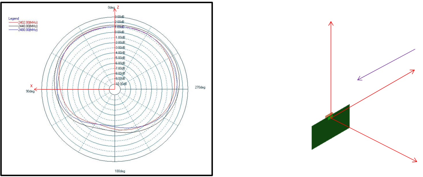
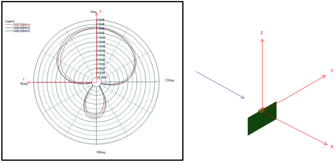
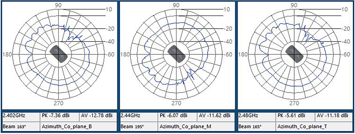
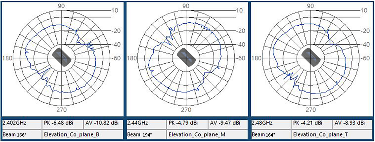
Antenna Characteristics
Lyra 24P Module Antenna
Typical performance curves indicate typical characterized performance under the stated conditions.
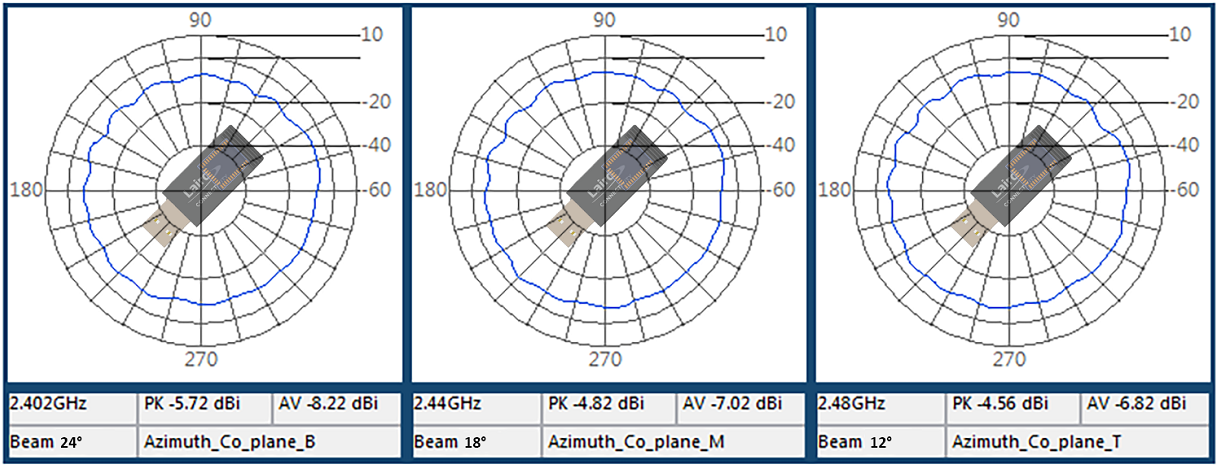
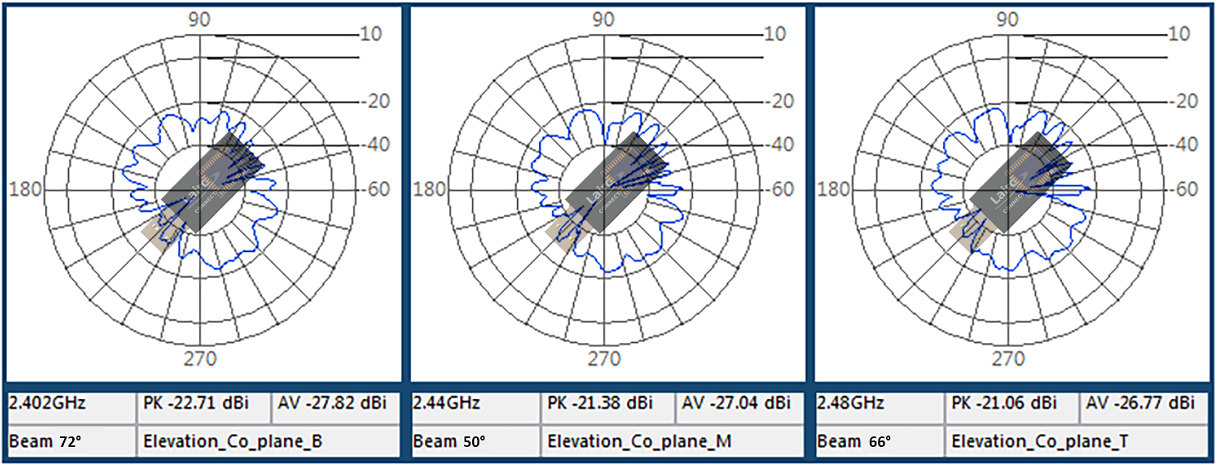
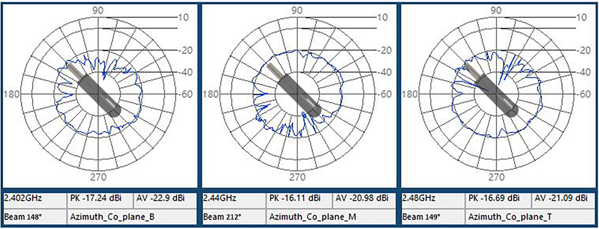
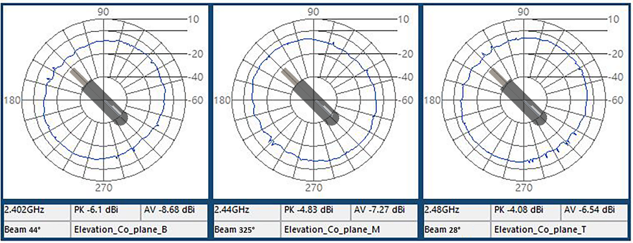
Typical Lyra 24P radiation patterns and efficiency for the integrated antenna under optimal operating conditions are plotted in the figures that follow. Antenna gain and radiation patterns have a strong dependence on the size and shape of the application PCB the module is mounted on, as well as on the proximity of any mechanical design to the antenna.
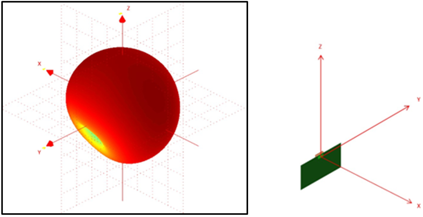
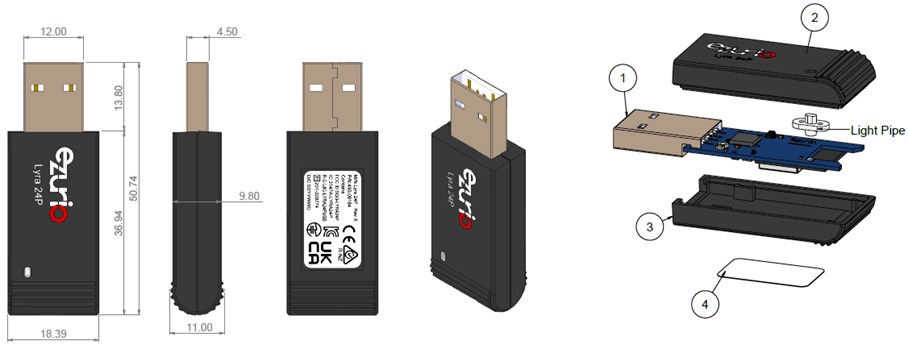
Lyra 24P USB Adapter
The Lyra 24P USB adaptor uses the 453-000145 - Lyra 24P Series - Bluetooth v5.4 PCB Module (20dBm) with integrated antenna module which has 1.82dBi antenna gain.
The Lyra 24P USB adaptor small PCB size (small ground plane) limits the radiated antenna performance. See Lyra 24P USB adaptor antenna patterns in X, Y and Z orientations for 3 channels.
| Antenna Gain in dBi | 2402MHz Peak | 2402MHz Average | 2440MHz Peak | 2440MHz Average | 2480MHz Peak | 2480MHz Average |
|---|---|---|---|---|---|---|
| X plane Azimuth | -5.72dBi | -8.22dBi | -4.82dBi | -7.02dBi | -4.56dBi | -6.82dBi |
| X plane Elevation | -22.71dBi | -27.82Bi | -21.38dBi | -27.04dBi | -21.06dBi | -26.77dBi |
| Y plane Azimuth | -17.24dBi | -22.9dBi | -16.11dBi | -20.98dBi | -16.69dBi | -21.09dBi |
| Y plane Elevation | -6.1dBi | -8.68dBi | -4.83dBi | 7.27dBi | -4.08dBi | -6.54dBi |
| Z plane Azimuth | -7.36dBi | -12.78dBi | -6.07dBi | -11.62dBi | -5.61dBi | -11.18dBi |
| Z plane Elevation | -6.48dBi | -10.82dBi | -4.79dBi | -9.47dBi | -4.21dBi | -8.93dBi |
Circuit (Overview and Checklist)
PCB Layout
PCB Layout on Host PCB - General
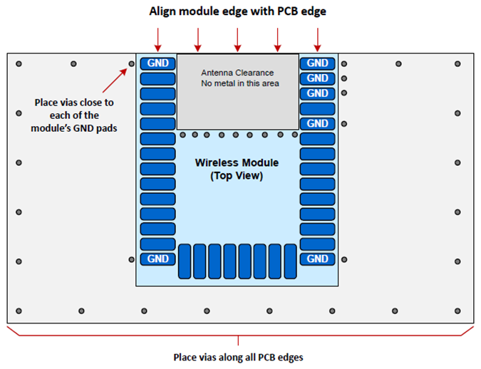
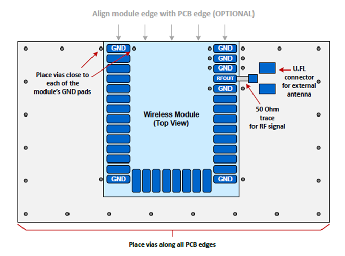
For optimal performance of the Lyra 24P:
Place the module aligned to the edge of the application PCB, as illustrated in the figures below.
- Optional on the module with the RF pin.
- Leave the antenna clearance area void of any traces, components, or copper on all layers of the application PCB if you are going to use the built-in antenna.
- Antenna clearance area is not necessary if you are using an external antenna attached to the RF pin.
- RFOUT can be left floating if not used.
Antennas external to the module, either connectorized off-the-shelf antennas or PCB trace antennas, must be well-matched to 50 Ω.
- For external antenna use cases, use a 50 Ω grounded coplanar transmission line to trace the signal from the RF pin to an external MHF4 RF connector if applicable (see Recommended Layout for Lyra 24P Using External Antenna, below).
- A general rule is to use 50 Ω transmission lines where the length of the RF trace is longer than λ/16 at the fundamental frequency, which for 2.4 GHz is approximately 3.5 mm.
- An IPEX MHF4 RF connector can be used in the host PCB for the connection to an external antenna. The use of a MHF4 connector is also recommended for conductive tests. The integrator must use a unique connector, such as a “reverse polarity SMA” or “reverse thread SMA”, if detachable antenna is offered with the host chassis. This is especially required for the FCC and ISED approvals to remain valid, and any other kind of direct connector to the antenna might require a permissive change.
- A trace length of 1.84 mm was used in the certifications host board to connect the module RF pin to the MHF4 RF connector.
- For reference, Layer 2 drawing in External Antenna Integration shows a set of parameters for a 50 Ω trace. Trace impedance should always be matched to the particular stack-up used on the host board.
Connect all ground pads directly to a solid ground plane.
Place the ground vias as close to the ground pads as possible.
Avoid plastic or any other dielectric material in contact with the antenna.
The figure below illustrates layout scenarios that will lead to severely degraded RF performance for the module.
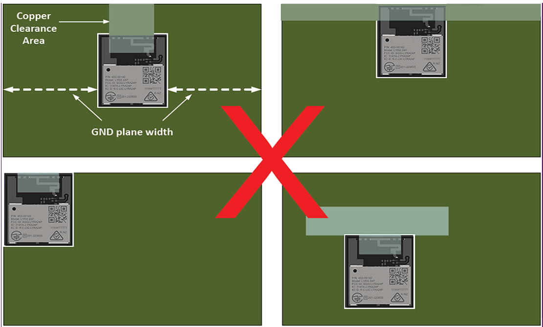
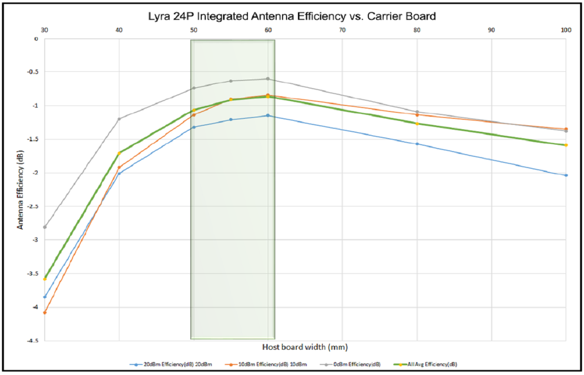
The width of the GND plane to the sides the module will impact the efficiency of the built in antenna. To achieve optimal performance, a GND plane width of 55-60 mm is recommended. See Lyra 24P Integrated Antenna for reference.
Proximity to Human Body
Placing the module in contact with or very close to the human body will negatively impact antenna efficiency and reduce range.
Antenna Keep-Out on Host PCB
External Antenna Integration
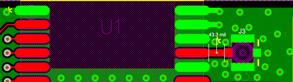
Lyra 24P 50 Ohms RF Track Design for Connecting External Antenna with the Lyra 24P Module, 20dBm, RF Pad Variant (453-00148)
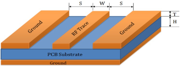
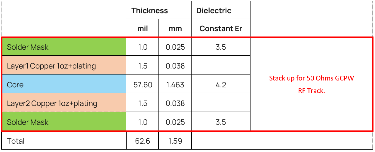
Lyra 24P module can be used with external antennas (certified by Ezurio), and requires a 50 Ohm RF trace (GCPW, that Grounded Coplanar Waveguide) to be designed to run from Lyra 24P module RFOUT (pin33) to a RF antenna connector (IPEX MHF4) on host PCB. The 50 Ohms RF track design and length MUST be copied (as specified in this section). Lyra 24P module GND pin32 and GND pin34 used to support GCPW 50Ohm RF trace.
Checklist for SCH
| Lyra 24P External antenna connection SCH | Lyra 24P External antenna connection PCB |
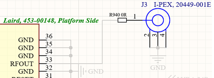 |  |
Lyra 24P for External antenna connection host PCB 50-Ohm RF trace schematic with MHF4 RF connector
Layer1 (RF Track and RF GND)
Layer2 (RF GND)
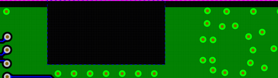
50-Ohm RF trace design (Layer1 and Layer2) on DVK-Lyra 24P development board 453-00148-K1 (or host PCB) for use with Lyra 24P (453-00148) module
Checklist for PCB:
- MUST use a 50-Ohm RF trace (GCPW, that is Grounded Coplanar Waveguide) from RFOUT pad (pin33) of the Lyra 24P module (453-00148) to RF antenna connector (IPEX MHF4 Receptable (MPN: 20449-001E)) on host PCB.
- To ensure regulatory compliance, MUST follow exactly the following considerations for 50-Ohms RF trace design and test verification:
Note 1: The plating (ENIG) above base 1ounce copper is not listed, but plating expected to be ENIG.
The 50-Ohms RF trace design MUST be Grounded Coplanar Waveguide (GCPW) with
- Layer1 RF track width (W) of 20 mil and
- Layer1 gap (S) to GND of 5 mil and where the
- Layer1 to Layer 2 dielectric thickness (H) MUST be 57.6 mil (dielectric constant Er 4.2).
- Further the Layer1 base copper must be 1-ounce base copper (that is 1.5 mil) plus the plating and
- Layer1 MUST be covered by solder mask of 1.0 mil thickness (dielectric constant Er 3.5).
- The 50-Ohms RF trace design MUST follow the PCB stack-up shown in the table above. (Layer1 to Layer2 thickness MUST be identical to the Lyra 24P development board).
- The 50-Ohms RF track should be a controlled-impedance trace e.g., ±10%.
- The 50-Ohms RF trace length MUST be identical (as seen in Layer 2 drawing above) (43.3mil) to that on the Lyra 24P development board from Lyra 24P module RFOUT RF pad (pin33) to the RF connector IPEX MHF4 Receptable (MPN: 20449-001E).
- Place GND vias regularly spaced either side of 50-Ohms RF trace to form GCPW (Grounded coplanar waveguide) transmission line (as shown in Layer 2 drawing above) and use Lyra 24P module GND pin32, GND pin34.
- Use spectrum analyzer to confirm the radiated (and conducted) signal is within the certification limit.
External Antenna Integration with the Lyra 24P Module, 20dBm, RF pad variant (453-00148)
Please refer to the Lyra 24P Regulatory Information Guide for details on using Lyra 24P module with external antennas in each regulatory region. This guide is available at https://www.ezurio.com/documentation/regulatory-information-lyra-24p.
The Lyra 24P has been designed to operate with the below external antennas (with a maximum gain of 2.0dBi). The required antenna impedance is 50 ohms. See Certified Antennas. External antennas improve radiation efficiency.
Host Platform Implementation Details
Network Co-Processor (NCP) Application with UART Host
The Lyra 24P can be controlled over the UART interface as a peripheral to an external host processor. Typical power supply, programming/debug interface, and host interface connections are shown in the figure below. For more details, see AN958: Debugging and Programming Interfaces for Custom Designs.
Note: For boot pin, see Boot section.
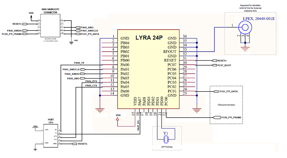
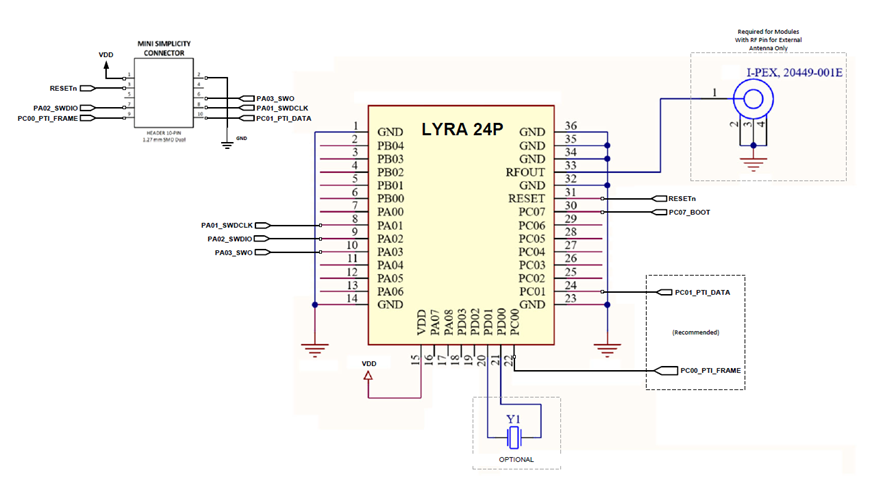
SoC Application
The Lyra 24P can be used in a stand-alone SoC configuration without an external host processor. Typical power supply and programming/debug interface connections are shown in the figure below. For more details, see AN958: Debugging and Programming Interfaces for Custom Designs.
Boot
The BOOT pin is used to determine when execution of the bootloader is required. Upon reset, execution of the bootloader begins. The state of the BOOT pin is read immediately upon start-up of the bootloader. If LOW, execution of the bootloader continues, facilitating firmware update via the UART. If the BOOT pin is HIGH, the bootloader will stop execution and pass control to the main application firmware.
Reset
The Lyra 24P can be reset by pulling the RESET line low, by the internal watchdog timer, or by software command.
The reset state does not provide power saving functionality and it is not recommended as a means to conserve power.
Debug
The Lyra 24P supports hardware debugging via 4-pin JTAG or 2-pin serial-wire debug (SWD) interfaces. It is recommended to expose the debug pins in your own hardware design for firmware update and debug purposes. The table below lists the required pins for JTAG and SWD debug interfacing, which are also presented in Section Alternate Function Table.
If JTAG interfacing is enabled, the module must be power cycled to return to a SWD debug configuration if necessary.
| Pin Name | JTAG Signal | SWD Signal | Comments |
|---|---|---|---|
| PA04 | TDI | N/A | This pin is disabled after reset. Once enabled the pin has a built-in pull-up. |
| PA03 | TDO | N/A | This pin is disabled after reset. |
| PA02 | TMS | SWDIO | Pin is enabled after reset and has a built-in pull-up. |
| PA01 | TCK | SWCLK | Pin is enabled after reset and has a built-in pull-down. |
Packet Trace Interface (PTI)
The Lyra 24P integrates a true PHY-level packet trace interface (PTI) peripheral that can capture packets non-intrusively to monitor and log device and network traffic without burdening processing resources in the module's SoC. The PTI generates two output signals that can serve as a powerful debugging tool, especially in conjunction with other hardware and software development tools available from Silicon Labs. The PTI_DATA and PTI_FRAME signals can be accessed through any GPIO on ports C and D (see FRC.DOUT and FRC.DFRAME peripheral resources in Pin Definitions.
Application Note for Surface Mount Modules
PCB Land Pattern
Dimensions for 450-00184 Lyra 24P – Bluetooth v5.4 USB Adaptor (20dBm) with Integrated Antenna (Silicon Labs EFR32BG24)
The Lyra 24P USB dongle User Guide is available on the Lyra 24 Series product page:
https://www.ezurio.com/lyra24-series
Module Label Marking
The figure below shows the module markings engraved on the RF shield.
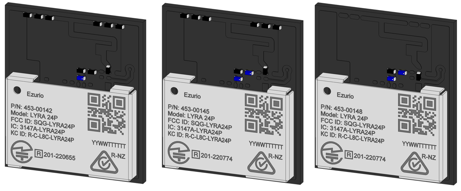
The package marking consists of:
- P/N - Part number designation
- Model: Lyra 24P Model number designation
QR Code: YYWWTTTTTT
- YY – Last two digits of the assembly year.
- WW – Two-digit workweek when the device was assembled.
- TTTTTT – Manufacturing trace code. The first two letters are the ID of the manufacturer followed by 4 digits of trace code.
Date code: YYWWTTTTTT
- YY – Last two digits of the assembly year.
- WW – Two-digit workweek when the device was assembled.
- TTTTTT – Manufacturing trace code. The first two letters are the ID of the manufacturer followed by 4 digits of trace code.
- Certification marks such as the CE logo, FCC, and IC IDs, etc as per above image.
USB Adapter Label Marking
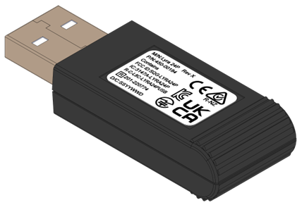
The package marking consists of:
- P/N - Part number designation
- Model: Lyra 24P Model number designation
Date Code: YYWWTTTTTT
- YY – Last two digits of the assembly year.
- WW – Two-digit workweek when the device was assembled.
- TTTTTT – Manufacturing trace code. The first two letters are the ID of the manufacturer followed by 4 digits of trace code.
- Certification marks such as the CE logo, FCC, and IC IDs, etc as per above image.
Tape and Reel
Lyra 24P modules are delivered to the customer in cut tape (250 pcs) or reel (1000 pcs) packaging with the dimensions below. All dimensions are given in mm unless otherwise indicated.
Recommended Stencil Aperture
Reflow Parameters/ Soldering
- Optimal solder reflow profile depends on solder paste properties and should be optimized as part of an overall process development.
- It is important to provide a solder reflow profile that matches the solder paste supplier's recommendations.
- Temperature ranges beyond that of the solder paste supplier's recommendation could result in poor solderability.
- All solder paste suppliers recommend an ideal reflow profile to give the best solderability.
Miscellaneous
Cleaning
In general, cleaning the populated modules is strongly discouraged. Residuals under the module cannot be easily removed with any cleaning process.
- Cleaning with water can lead to capillary effects where water is absorbed into the gap between the host board and the module. The combination of soldering flux residuals and encapsulated water could lead to short circuits between neighboring pads. Water could also damage any stickers or labels.
- Cleaning with alcohol or a similar organic solvent will likely flood soldering flux residuals into the RF shield, which is not accessible for post-washing inspection. The solvent could also damage any stickers or labels.
- Ultrasonic cleaning could damage the module permanently.
Rework
The Lyra 24P module can be unsoldered from the host board if the Moisture Sensitivity Level (MSL) requirements are met as described in this datasheet.
Never attempt a rework on the module itself, i.e. replacing individual components. Such actions terminate warranty coverage.
Environmental and Reliability
Environmental Requirements
Handling Conditions
The Lyra 24P module contain a highly sensitive electronic circuitry. Handling without proper ESD protection may damage the module permanently.
Moisture Sensitivity Level (MSL)
Per J-STD-020, devices rated as MSL 4 and not stored in a sealed bag with desiccant pack should be baked prior to use.
Devices are packaged in a Moisture Barrier Bag with a desiccant pack and Humidity Indicator Card (HIC). Devices that will be subjected to reflow should reference the HIC and J-STD-033 to determine if baking is required.
If baking is required, refer to J-STD-033 for bake procedure.
Required Storage Conditions
Per J-STD-033, the shelf life of devices in a Moisture Barrier Bag is 12 months at <40C and <90% room humidity (RH).
Do not store in salty air or in an environment with a high concentration of corrosive gas, such as Cl2, H2S, NH3, SO2, or NOX. Do not store in direct sunlight.
The product should not be subject to excessive mechanical shock.
Repeated Reflow Soldering
Only a single reflow soldering process is encouraged for host boards.
Reliability Tests
Climatic and Dynamic
Climatic and Dynamic Reliability Test Results for Lyra 24P Modules
| Test Item | Specification | Standard | Test Result |
|---|---|---|---|
| Step 1: Pre-conditioning | Pre-check:
Pre-conditioning:
Post-check:
| JESD22-A113 | Pass |
| Step 2: Temperature Cycling Non-operating |
10. Shock to 85°C within ramp rate 15 ℃/minute 11. Dwell on 85°C for 15 minutes 12. Shock to -40°C within ramp rate 15 degree C/minute 13. Repeat step 1-4 and stop to check functions at 500/ 700 cycles | JESD22-A113 | Pass |
| Mechanical Shock Non-operating |
| JEDEC 22-B110B.01 (2019) | Pass |
Climatic and Dynamic Reliability Test Results for Lyra 24P USB Adapter
| Test Item | Specification | Standard | Test Result |
|---|---|---|---|
| Thermal Shock |
| *JESD22-A106 *IEC 60068-2-14 for dwell time and number of cycles | Pass |
| Vibration Non-operating Unpackaged device |
| JEDEC 22-B103B (2016) | Pass |
| Mechanical Shock Non-operating Unpackaged device |
| JEDEC 22-B110B.01 (2019) | Pass |
Reliability Prediction
MTBF Prediction for Lyra 24P Modules
| Ezurio Part Number | Environment | Test Result 40 ℃ (Hours) |
| 453-00142R 453-00142C 453-00145R 453-00145C 453-00148R 453-00148C | Ground, Fixed, Uncontrolled | 17,000,000 |
| Ezurio Part Number | Environment | Test Result 105 ℃ (Hours) |
| 453-00142R 453-00142C 453-00145R 453-00145C 453-00148R 453-00148C | Ground, Fixed, Uncontrolled | 900,000 |
MTBF Prediction for Lyra 24P USB Adapter
| Ezurio Part Number | Environment | Test Result 40 ℃ (Hours) |
| 450-00184 | Ground, Fixed, Uncontrolled Ground, Mobile | 1,311,381.23 2,608,428.88 |
| Ezurio Part Number | Environment | Test Result 85 ℃ (Hours) |
| 450-00184 | Ground, Fixed, Uncontrolled Ground, Mobile | 148,641.17 279,361.02 |
Regulatory, Qualification & Certifications
Regulatory Approvals
Please refer to the Lyra 24P Regulatory Information Guide for details on using Lyra 24P module with external antennas in each regulatory region. This guide will be available at: http://www.ezurio.com/lyra24-series.
The Lyra 24P holds current certifications in the following countries:
| Country/Region | Regulatory ID |
|---|---|
| USA (FCC) | SQG-LYRA24P |
| Canada (ISED) | 3147A-LYRA24P |
| UK (UKCA) | N/A |
| EU | N/A |
| Japan (MIC) | 201-220655 (+10 dBm) / 201-220774 (+20 dBm) |
| Korea (KC) | R-C-L8C-LYRA24P (Module) R-C-L8C-LYRA24PUSB (USB Adapter) |
| Australia (AS) | N/A |
| New Zealand (NZS) | N/A |
Maximum Regulatory Certified RF TX Power per Country - 453-00148 Lyra 24P Series - Bluetooth v5.4 PCB Module (20dBm) w/ RF Trace Pad
For shipped AT Firmware
AT firmware implements RF TX power settings per country highlighted in below table and per country sections have detailed information.
| Country and implementation | Global | EU | UK | USA | Canada | Australia | New Zealand | Japan | South Korea | |
|---|---|---|---|---|---|---|---|---|---|---|
| AT FW | Region code | GL | EU | UK | US | CA | AU | NZ | JP | SK |
| AFH FW module? | Turned on or off | on | on | on | on | on | on | on | on | on |
20dBm mode (>15 BLE channels free) | Target TX power conducted | 17dBm | 17dBm | 17dBm | 17dBm | 17dBm | 17dBm | 17dBm | 17dBm | 17dBm |
| Antenna Gain setting. | 3.5dBi | 3.5dBi | 3.5dBi | 3.5dBi | 3.5dBi | 3.5dBi | 3.5dBi | 3.5dBi | 3.5dBi | |
| TX power setting | 20dBm | 20dBm | 20dBm | 20dBm | 20dBm | 20dBm | 20dBm | 20dBm | 20dBm | |
| Turn off CH39 2480MHz | yes | no | no | yes | yes | no | no | no | no | |
| 10dBm mode (<15 BLE channels free) | Target TX power conducted | 7dBm | 7dBm | 7dBm | 7dBm | 7dBm | 7dBm | 7dBm | 7dBm | 7dBm |
| Antenna Gain setting. | 3.5dBi | 3.5dBi | 3.5dBi | 3.5dBi | 3.5dBi | 3.5dBi | 3.5dBi | 3.5dBi | 3.5dBi | |
| TX power setting | 10dBm | 10dBm | 10dBm | 10dBm | 10dBm | 10dBm | 10dBm | 10dBm | 10dBm |
453-00148 Lyra 24P – Bluetooth v5.4 PCB Module (20dBm) with RF Trace Pad is shipped with AT firmware where the radio regulatory region “global” is set which is lowest common settings across RF TX power across certified countries.
To switch to the specific radio regulatory region country of USA, Canada, Europe, UK, Australia, New Zealand, Japan, and South Korea, customer can use appropriate AT command for setting the radio regulatory region per country.
For Customers C Code Development
Customers developing with C Code – Full software development with Silicon Labs SDK and Toolchain, MUST implement the RF TX power settings per country and other parameters mentioned in this section.
AFH Firmware Module
For BLE 20dBm modules, and whenever for radio regulatory declared radio as FHSS, the Silabs AFH FW module MUST be enabled. See Silabs AFH firmware module (in Silabs BLE stack) operation description: https://docs.silabs.com/bluetooth/5.0/general/system-and-performance/adaptive-frequency-hopping
Below is basic summary:- Does spectral scanning every one second (takes about 10ms to scan 40 BLE channels) AFTER first transmission (after an advertisement is sent)
- If RF interference is present on a channel (above -71dBm), then that channel is NOT used and is blacklisted for at least 8 afh_scan_intervals
- You are allowed to use TX power above +10 dBm when AFH is enabled and at least 15 channels are available
- Note that high transmit power is only allowed once for each channel after a measurement on that channel occurs. In other words, if you use the same channel multiple times for transmitting within afh_scan_interval, the second and consecutive transmission will use +10 dBm. If you have a short connection interval and long afh_scan_interval, this can easily happen,
- Other limitations:
“When AFH is applied, the length of the connection events (not to be confused with the connection interval) is limited to 40 ms. In other words, in every connection interval you can send packets only for 40 ms. This is usually not a problem because it takes around 2.5 ms to transmit a packet with 251B payload. However, to achieve maximum throughput with unacknowledged data transmission (see Throughput with Bluetooth Low Energy, you have to take into account this limitation. For example, if you have 100 ms connection interval, you can send packets only 40% of the time. To achieve maximum throughput, decrease your connection interval to 40 ms or lower.”
- AFH FW module has high 20dBm mode and lower 10dBm mode (in both cases actual RF TX power is lower as per Ezurio certified tables).
- AFH FW module uses high (20dBm) mode when at least 15 BLE channels are available.
- AFH FW module uses low (10dBm) mode If the number of available BLE channels are less than 15. E.g. when using legacy BLE Advert (which has only 3 BLE channels namely 2402, 2440, 2480MHz), then the AFH FW module drops to 10dBm mode.
NOTE: In both cases actual RF TX power is lower as per below Ezurio certified table. - Why is Antenna Gain setting used? Implemented (in AT firmware) lower RF TX power (for both 20dBm and 10dBm modes) than certified in 10dBm mode. Reason for this is the 10dBm mode TX power setting is hardcoded to 10dBm (by Silabs), so to achieve Ezurio certified TX power e.g. 7dBm for CE (which is lower than 10dBm for CE), the method of using Antenna Gain setting is used to produce the actual TX power that Ezurio certified in the 10dBm mode. Since Antenna Gain setting applies to both 10dBm mode and 20dBm mode and all countries, so it impacts RF TX power across both modes (20dBm and 10dBm modes) and countries.
Silabs BLE SDK 5.0.0.0 GA (December 14, 2022) version does NOT allow TX power setting in 10dBm mode to be modified.
Europe (CE), UK (UKCA), Australia (RCM, New Zealand (RCM) Radio RF TX power Table
20dBm mode - Europe (CE), UK (UKCA), Australia (RCM, New Zealand (RCM) Radio TX power table
| Module Ezurio Part number | 453-00148 | |||||||
| Description | Lyra 24P - Bluetooth v5.4 PCB Module (20dBm) with RF Trace Pad (Silicon Labs EFR32BG24) | |||||||
| Antenna Gain (dBi) | 2.0dBi peak external antenna | |||||||
| Radio Regulatory country: | Europe (CE), UK (UKCA), Australia (RCM) and New Zealand (RCM) | |||||||
| Declared as FHSS or DTS? | FHSS (uses Silabs AFH FW module ON) | |||||||
| AFH FW module? | AFH firmware module turned ON. | |||||||
| Silabs BLE SDK: Silabs Gecko SDK Suite: | 5.0.0.0 GA (December 14, 2022). 4.2 (December 14, 2022). | |||||||
| 20dBm Mode. Declared as FHSS. | CERTIFIED maximum conducted RF TX power per BLE PHY | CERTIFIED LOWEST COMMON RF TX power setting across BLE PHY’s, other restrict… | IMPLEMENTED in Ezurio AT FW or Customer MUST implement in customers own developed C-code. AFH firmware module turned ON. | |||||
| NOTE 1 | NOTE 2 | NOTE 3 | NOTE 4A | NOTE 4B | ||||
| BLE PHY | Physical channel (channel Index) | Frequency (MHz) channel centre. | Certified conducted Maximum TX Power setting dBm | Certified measured Conducted Peak POWER (dBm) | Certified Lowest common conducted RF TX power setting across all 4 BLE data rates. | Target RF TX power conducted to implement in FW. Other restrictions (if any). | Antenna Gain setting in FW | Conducted TX power setting in FW |
| BLE 1Mbps | CH0 (CH37) | 2402 MHz | 17dBm | 17.41dBm | 17dBm | 17dBm | 3.5dBi | 20dBm |
| CH39 (CH39) | 2480 MHz | 17dBm | 17.14 dBm | 17dBm | 17dBm | 3.5dBi | 20dBm | |
| BLE 2Mbps | CH1 (CH0) | 2404 MHz | 17dBm | 17.44dBm | 17dBm | 17dBm | 3.5dBi | 20dBm |
| CH38 (CH36) | 2478 MHz | 17dBm | 17.22dBm | 17dBm | 17dBm | 3.5dBi | 20dBm | |
| BLE 125kbps | CH0 (CH37) | 2402 MHz | 17dBm | 17.40dBm | 17dBm | 17dBm | 3.5dBi | 20dBm |
| CH39 (CH39) | 2480 MHz | 17dBm | 17.10dBm | 17dBm | 17dBm | 3.5dBi | 20dBm | |
| BLE 500kbps | CH0 (CH37) | 2402 MHz | 17dBm | 17.40dBm | 17dBm | 17dBm | 3.5dBi | 20dBm |
| CH39 (CH39) | 2480 MHz | 17dBm | 17.15dBm | 17dBm | 17dBm | 3.5dBi | 20dBm | |
10dBm mode - Europe (CE), UK (UKCA), Australia (RCM, New Zealand (RCM) Radio TX power table
10dBm mode. Declared as DTS. | CERTIFIED maximum conducted RF TX power per BLE PHY | CERTIFIED LOWEST COMMON RF TX power setting across BLE PHY’s, other restrict… | IMPLEMENTED in Ezurio AT FW or customer MUST implement in customers own developed C-code. AFH firmware module turned ON. | |||||
| NOTE 1 | NOTE 2 | NOTE 3 | NOTE 4A | NOTE 4B | ||||
| BLE PHY | Physical channel (channel Index) | Frequency (MHz) channel centre. | Certified conducted Maximum TX Power setting dBm | Certified Measured Conducted Peak POWER (dBm) | Certified Lowest common conducted RF TX power setting across all 4 BLE data rates. | Target RF TX power conducted to implement in FW. Other restrictions (if any). | Antenna Gain setting in FW | TX power setting in FW |
| BLE 1Mbps | CH0 (CH37) | 2402 MHz | 7dBm | 7.58dBm | 7dBm | 7dBm | 3.5dBi | 10dBm |
| CH39 (CH39) | 2480 MHz | 7dBm | 7.20dBm | 7dBm | 7dBm | 3.5dBi | 10dBm | |
| BLE 2Mbps | CH1 (CH0) | 2404 MHz | 7dBm | 7.59dBm | 7dBm | 7dBm | 3.5dBi | 10dBm |
| CH38 (CH36) | 2478 MHz | 7dBm | 7.25dBm | 7dBm | 7dBm | 3.5dBi | 10dBm | |
| BLE 125kbps | CH0 (CH37) | 2402 MHz | 7dBm | 7.58dBm | 7dBm | 7dBm | 3.5dBi | 10dBm |
| CH39 (CH39) | 2480 MHz | 7dBm | 7.20dBm | 7dBm | 7dBm | 3.5dBi | 10dBm | |
| BLE 500kbps | CH0 (CH37) | 2402 MHz | 7dBm | 7.58dBm | 7dBm | 7dBm | 3.5dBi | 10dBm |
| CH39 (CH39) | 2480 MHz | 7dBm | 7.20dBm | 7dBm | 7dBm | 3.5dBi | 10dBm | |
Notes:
- NOTE 1: CERTIFIED maximum conducted RF TX power per BLE PHY in 20dBm mode or 10dBm mode tables. This is not what is implemented in AT firmware, this is what was certified only.
- NOTE 2: Certified Lowest common TX power setting across BLE PHY’s. This lowest common TX power setting is stated since we do not use per BLE RF TX power setting in AT firmware, but same TX power setting across all 4 BLE PHY’s.
- NOTE 3: IMPLEMENT in AT firmware target RF TX power conducted. This target actual implemented in AT firmware. For CE, UKCA, RCM (Australia and New Zealand), this is actual target 17dBm conducted (in 20dBm mode) and 7dBm conducted (in 10dBm mode). To implement that, NOTE 4A defines what Antenna Gain setting MUST be used and NOTE 4B defines what TX power setting MUST be used.
NOTE 4: IMPLEMENTED in AT firmware (or MUST implement in customers own developed C-code) the Actual target RF TX power conducted:
- NOTE 4A: the Antenna Gain setting of 3.5dBi and
- NOTE 4B: the TX power setting to 20dBm (in 20dBm mode) and 10dBm (in 10dBm mode) which results in:
Target Actual RF TX power (dBm) = TX power setting (dBm) - Antenna Gain setting(dBi)
17dBm = 20dBm – 3.5dBi
7dBm = 10dBm – 3.5dBi
USA (FCC), Canada (ISED) Radio RF TX power Table
20dBm mode - USA (FCC), Canada (ISED) Radio TX power table
| Module Ezurio Part Number | 453-00148 | |||||||
| Description | Lyra 24P - Bluetooth v5.4 PCB Module (20dBm) with RF Trace Pad (Silicon Labs EFR32BG24) | |||||||
| Antenna Gain (dBi) | 2.0dBi peak external antenna | |||||||
| Radio Regulatory Country: | USA (FCC), CANADA (ISED) | |||||||
| Declared as FHSS or DTS? | FHSS (uses Silabs AFH FW module ON) | |||||||
| AFH FW Module? | AFH firmware module turned ON. | |||||||
| Silabs BLE SDK: Silabs Gecko SDK Suite: | 5.0.0.0 GA (December 14, 2022). 4.2 (December 14, 2022). | |||||||
20dBm mode. FHSS. | CERTIFIED maximum conducted RF TX power per BLE PHY | CERTIFIED LOWEST COMMON RF TX power setting across BLE PHY’s, other restrict… | IMPLEMENTED in Ezurio AT FW Or customer MUST implement in customers own developed C-code. AFH firmware module turned ON.
| |||||
| NOTE 1 | NOTE 2 | NOTE 3 | NOTE 4A | NOTE 4B | ||||
| BLE PHY | Physical channel (channel Index) | Frequency (MHz) channel centre. | Certified conducted Maximum TX Power setting dBm | Certified Measured Conducted Peak POWER (dBm) | Certified Lowest common conducted RF TX power setting across all 4 BLE data rates. | Target RF TX power conducted to implement in FW. Other restrictions (if any). | Antenna Gain setting in FW | TX power setting in FW |
| BLE 1Mbps | CH0 (CH37) | 2402MHz | 20dBm | 19.95dBm | 17dBm | 17dBm | 3.5dBi | 20dBm |
| CH19 (CH17) | 2440MHz | 20dBm | 19.93dBm | 17dBm | 17dBm | 3.5dBi | 20dBm | |
| CH38 (CH36) | 2478MHZ | 18dBm | 18.10dBm | 17dBm | 17dBm | 3.5dBi | 20dBm | |
| CH39 (CH39) | 2480MHz | 15dBm | 15.53dBm | Turn OFF CH39 (2480MHz) | Turn OFF CH39 (2480MHz) in FW. | |||
| BLE 2Mbps | CH1 (CH0) | 2404MHz | 20dBm | 19.94dBm | 17dBm | 17dBm | 3.5dBi | 20dBm |
| CH19 (CH17) | 2440MHz | 20dBm | 19.92dBm | 17dBm | 17dBm | 3.5dBi | 20dBm | |
| CH38 (CH36) | 2478MHz | 17dBm | 17.21dBm | 17dBm | 17dBm | 3.5dBi | 20dBm | |
| BLE coded PHY 125kbps | CH0 (CH37) | 2402MHz | 20dBm | 19.94dBm | 17dBm | 17dBm | 3.5dBi | 20dBm |
| CH19 (CH17) | 2440MHz | 20dBm | 19.91dBm | 17dBm | 17dBm | 3.5dBi | 20dBm | |
| CH38 (CH36) | 2478MHz | 18dBm | 18.09dBm | 17dBm | 17dBm | 3.5dBi | 20dBm | |
| CH39 (CH39) | 2480MHz | 15dBm | 15.52dBm | Turn OFF CH39 (2480MHz) | Turn OFF CH39 (2480MHz) in FW. | |||
| BLE coded PHY 500kbps | CH0 (CH37) | 2402MHz | 20dBm | 19.93dBm | 17dBm | 17dBm | 3.5dBi | 20dBm |
| CH19 (CH17) | 2440MHz | 20dBm | 19.90dBm | 17dBm | 17dBm | 3.5dBi | 20dBm | |
| CH38 (CH36) | 2478MHz | 18dBm | 18.08dBm | 17dBm | 17dBm | 3.5dBi | 20dBm | |
| CH39 (CH39) | 2480MHz | 15dBm | 15.51dBm | Turn OFF CH39 (2480MHz) | Turn OFF CH39 (2480MHz) in FW. | |||
10dBm mode - USA (FCC), Canada (ISED) Radio TX power table
10dBm mode. DTS. | CERTIFIED maximum conducted RF TX power per BLE PHY | CERTIFIED LOWEST COMMON RF TX power setting across BLE PHY’s, other restrict… | Implemented in Ezurio AT FW or customer MUST implement in customers own developed C-code. AFH firmware module turned ON. | |||||
| NOTE 1 | NOTE 2 | NOTE 3 | NOTE 4A | NOTE 4B | ||||
| BLE PHY | Physical channel (channel Index) | Frequency (MHz) channel centre. | Certified conducted Maximum TX Power setting dBm | Certified Measured Conducted Peak POWER (dBm) | Certified Lowest common conducted RF TX power setting across all 4 BLE data rates. | Target RF TX power conducted to implement in FW. Other restrictions (if any). | Antenna Gain setting in FW | TX power setting in FW |
| BLE 1Mbps | CH0 (CH37) | 2402MHz | 10dBm | 10.32dBm | 10dBm | 7dBm | 3.5dBi | 10dBm |
| CH19 (CH17) | 2440MHz | 10dBm | 10.18dBm | 10dBm | 7dBm | 3.5dBi | 10dBm | |
| CH38 (CH36) | 2478MHz | 10dBm | 10.05dBm | 10dBm | 7dBm | 3.5dBi | 10dBm | |
| CH39 (CH39) | 2480MHz | 10dBm | 10.02dBm | 10dBm | 7dBm | 3.5dBi | 10dBm | |
| BLE 2Mbps | CH1 (CH0) | 2404MHz | 10dBm | 10.31dBm | 10dBm | 7dBm | 3.5dBi | 10dBm |
| CH19 (CH17) | 2440MHz | 10dBm | 10.17dBm | 10dBm | 7dBm | 3.5dBi | 10dBm | |
| CH38 (CH36) | 2478MHz | 10dBm | 10.03dBm | 10dBm | 7dBm | 3.5dBi | 10dBm | |
| BLE coded PHY 125kbps | CH0 (CH37) | 2402MHz | 10dBm | 10.30dBm | 10dBm | 7dBm | 3.5dBi | 10dBm |
| CH19 (CH17) | 2440MHz | 10dBm | 10.17dBm | 10dBm | 7dBm | 3.5dBi | 10dBm | |
| CH38 (CH36) | 2478MHz | 10dBm | 10.02dBm | 10dBm | 7dBm | 3.5dBi | 10dBm | |
| CH39 (CH39) | 2480MHz | 10dBm | 10.01dBm | 10dBm | 7dBm | 3.5dBi | 10dBm | |
| BLE coded PHY 500kbps | CH0 (CH37) | 2402MHz | 10dBm | 10.29dBm | 10dBm | 7dBm | 3.5dBi | 10dBm |
| CH19 (CH17) | 2440MHz | 10dBm | 10.16dBm | 10dBm | 7dBm | 3.5dBi | 10dBm | |
| CH38 (CH36) | 2478MHz | 10dBm | 10.02dBm | 10dBm | 7dBm | 3.5dBi | 10dBm | |
| CH39 (CH39) | 2480MHz | 10dBm | 10.01dBm | 10dBm | 7dBm | 3.5dBi | 10dBm | |
Notes:
- NOTE 1: CERTIFIED maximum conducted RF TX power per BLE PHY in 20dBm mode or 10dBm mode tables. This is not what is implemented in AT firmware, this is what was certified only.
- NOTE 2: Certified Lowest common TX power setting across BLE PHY’s is 17dBm AND BLE CH39 2480MHz is turned OFF. Why do we turn OFF BLE CH39 2480MHz is because theCH39 2480MHz RF TX power that FCC, ISED pass was achieved at 15dBm, which is lower than 17dBm achieved at some of the other BLE channels. To use the lowest common RF TX power setting of 17dBm AND MUST turn OFF BLE channel CH39 2480MHz.
- NOTE 3: IMPLEMENT in AT firmware target RF TX power conducted. This target actual implemented in AT firmware. For FCC (USA), ISED (Canada), this is actual 17dBm conducted (in 20dBm mode) and 7dBm conducted (in 10dBm mode). To implement that, NOTE 4A defines what Antenna Gain setting MUST be used and NOTE 4B defines what TX power setting MUST be used.
NOTE 4: IMPLEMENTED in AT firmware (or MUST implement in customers own developed C-code) the Actual target RF TX power conducted:
- NOTE 4A: the Antenna Gain setting of 3.5dBi and
- NOTE 4B: the TX power setting to 20dBm (in 20dBm mode) and 10dBm (in 10dBm mode) which results in:
Target Actual RF TX power (dBm) = TX power setting (dBm) - Antenna Gain setting(dBi)
17dBm = 20dBm – 3.5dBi
7dBm = 10dBm – 3.5dBi
Australia (RCM, New Zealand (RCM) Radio RF TX Power Table
Same as EU (CE). Refer to Europe (CE), UK (UKCA), Australia (RCM, New Zealand (RCM) Radio RF TX power Table.
Japan (MIC) Radio RF TX Power Table
20dBm mode - Japan (MIC) Radio TX power table
| Module Ezurio Part number | 453-00148 | |||||||
| Description | Lyra 24P - Bluetooth v5.4 PCB Module (20dBm) with RF Trace Pad (Silicon Labs EFR32BG24) | |||||||
| Antenna Gain (dBi) | 2.0dBi peak external antenna | |||||||
| Radio Regulatory country: | Japan (MIC) | |||||||
| Declared as FHSS or DTS? | FHSS (uses Silabs AFH FW module ON) | |||||||
| AFH FW module? | AFH firmware module turned ON. | |||||||
| Silabs BLE SDK: Silabs Gecko SDK Suite: | 5.0.0.0 GA (December 14, 2022). 4.2 (December 14, 2022). | |||||||
20dBm mode. FHSS. | CERTIFIED maximum conducted RF TX power per BLE PHY | CERTIFIED LOWEST COMMON RF TX power setting across BLE PHY’s, other restrict… | IMPLEMENTED in Ezurio AT FW or customer MUST implement in customers own developed C-code. AFH firmware module turned ON. | |||||
| NOTE 1 | NOTE 2 | NOTE 3 | NOTE 4A | NOTE 4B | ||||
| BLE PHY | Physical channel (channel Index) | Frequency (MHz) channel centre. | Certified conducted Maximum TX Power setting dBm | Certified measured Conducted Peak POWER (dBm) | Certified Lowest common conducted RF TX power setting across all 4 BLE data rates. | Target RF TX power conducted to implement in FW. Other restrictions (if any). | Antenna Gain setting in FW | Conducted TX power setting in FW |
| BLE 1Mbps | CH0 (CH37) | 2402 MHz | 18dBm | 18.50dBm | 18dBm | 17dBm | 3.5dBi | 20dBm |
| CH39 (CH39) | 2480 MHz | 20dBm | 17.54dBm | 18dBm | 17dBm | 3.5dBi | 20dBm | |
| BLE 2Mbps | CH1 (CH0) | 2404 MHz | 18dBm | 18.22dBm | 18dBm | 17dBm | 3.5dBi | 20dBm |
| CH38 (CH36) | 2478 MHz | 18dBm | 18.02dBm | 18dBm | 17dBm | 3.5dBi | 20dBm | |
| BLE 125kbps | CH0 (CH37) | 2402 MHz | 18dBm | 18.49dBm | 18dBm | 17dBm | 3.5dBi | 20dBm |
| CH39 (CH39) | 2480 MHz | 18dBm | 18.30dBm | 18dBm | 17dBm | 3.5dBi | 20dBm | |
| BLE 500kbps | CH0 (CH37) | 2402 MHz | 18dBm | 18.21dBm | 18dBm | 17dBm | 3.5dBi | 20dBm |
| CH39 (CH39) | 2480 MHz | 18dBm | 18.10dBm | 18dBm | 17dBm | 3.5dBi | 20dBm | |
10dBm mode - Japan (MIC) Radio TX power table
10dBm mode. DTS. | CERTIFIED maximum conducted RF TX power per BLE PHY | CERTIFIED LOWEST COMMON RF TX power setting across BLE PHY’s, other restrict… | IMPLEMENTED in Ezurio AT FW or customer MUST implement in customers own developed C-code. AFH firmware module turned ON. | |||||
| NOTE 1 | NOTE 2 | NOTE 3 | NOTE 4A | NOTE 4B | ||||
| BLE PHY | Physical channel (channel Index) | Frequency (MHz) channel centre. | Certified conducted Maximum TX Power setting dBm | Certified Measured Conducted Peak POWER (dBm) | Certified Lowest common conducted RF TX power setting across all 4 BLE data rates. | Target RF TX power conducted to implement in FW. Other restrictions (if any). | Antenna Gain setting in FW | TX power setting in FW |
| BLE 1Mbps | CH0 (CH37) | 2402 MHz | 9dBm | 9.76dBm | 9dBm | 7dBm | 3.5dBi | 10dBm |
| CH39 (CH39) | 2480 MHz | 9dBm | 9.48dBm | 9dBm | 7dBm | 3.5dBi | 10dBm | |
| BLE 2Mbps | CH1 (CH0) | 2404 MHz | 9dBm | 9.74dBm | 9dBm | 7dBm | 3.5dBi | 10dBm |
| CH38 (CH36) | 2478 MHz | 9dBm | 9.49dBm | 9dBm | 7dBm | 3.5dBi | 10dBm | |
| BLE 125kbps | CH0 (CH37) | 2402 MHz | 9dBm | 9.73dBm | 9dBm | 7dBm | 3.5dBi | 10dBm |
| CH39 (CH39) | 2480 MHz | 9dBm | 9.43dBm | 9dBm | 7dBm | 3.5dBi | 10dBm | |
| BLE 500kbps | CH0 (CH37) | 2402 MHz | 9dBm | 9.76dBm | 9dBm | 7dBm | 3.5dBi | 10dBm |
| CH39 (CH39) | 2480 MHz | 9dBm | 9.46dBm | 9dBm | 7dBm | 3.5dBi | 10dBm | |
Notes:
- NOTE 1: CERTIFIED maximum conducted RF TX power per BLE PHY in 20dBm mode or 10dBm mode tables. This is not what is implemented in AT firmware, this is what was certified only.
- NOTE 2: Certified Lowest common TX power setting across BLE PHY’s. This lowest common TX power setting is stated since we do not use per BLE RF TX power setting in AT firmware, but same TX power setting across all 4 BLE PHY’s.
- NOTE 3: IMPLEMENT in AT firmware target RF TX power conducted. This target actual implemented in AT firmware. For Japan, this is the actual target 17dBm conducted (in 20dBm mode) and 7dBm conducted (in 10dBm mode). To implement that, NOTE 4A defines what Antenna Gain setting MUST be used and NOTE 4B defines what TX power setting MUST be used.
NOTE 4: IMPLEMENTED in AT firmware (or MUST implement in customers own developed C-code) the Actual target RF TX power conducted:
- NOTE 4A: the Antenna Gain setting of 3.5dBi and
- NOTE 4B: the TX power setting to 20dBm (in 20dBm mode) and 10dBm (in 10dBm mode) which results in:
Target Actual RF TX power (dBm) = TX power setting (dBm) - Antenna Gain setting(dBi)
17dBm = 20dBm – 3.5dBi
7dBm = 10dBm – 3.5dBi
South Korea Radio RF TX Power Table
20dBm mode - South Korea TX power table
| Module Ezurio Part number | 453-00148 | |||||||
| Description | Lyra 24P - Bluetooth v5.4 PCB Module (20dBm) with RF Trace Pad (Silicon Labs EFR32BG24) | |||||||
| Antenna Gain (dBi) | 2.0dBi peak external antenna | |||||||
| Radio Regulatory country: | South Korea (SK) | |||||||
| Declared as FHSS or DTS? | FHSS (uses Silabs AFH FW module ON) | |||||||
| AFH FW module? | AFH firmware module turned ON. | |||||||
| Silabs BLE SDK: Silabs Gecko SDK Suite: | 5.0.0.0 GA (December 14, 2022) 4.2 (December 14, 2022) | |||||||
| 20dBm mode. FHSS. | CERTIFIED maximum conducted RF TX power per BLE PHY | CERTIFIED LOWEST COMMON RF TX power setting across BLE PHY’s, other restrict… | IMPLEMENTED in Ezurio AT FW or customer MUST implement in customers own developed C-code. AFH firmware module turned ON. | |||||
| NOTE 1 | NOTE 2 | NOTE 3 | NOTE 4A | NOTE 4B | ||||
| BLE PHY | Physical channel (channel Index) | Frequency (MHz) channel centre. | Certified conducted Maximum TX Power setting dBm | Certified measured Conducted Peak POWER (dBm) | Certified Lowest common conducted RF TX power setting across all 4 BLE data rates. | Target RF TX power conducted to implement in FW. Other restrictions (if any). | Antenna Gain setting in FW | Conducted TX power setting in FW |
| BLE 1Mbps | CH0 (CH37) | 2402 MHz | 20dBm | 19.89dBm | 20dBm | 17dBm | 3.5dBi | 20dBm |
| CH39 (CH39) | 2480 MHz | 20dBm | 17.23dBm | 20dBm | 17dBm | 3.5dBi | 20dBm | |
| BLE 2Mbps | CH1 (CH0) | 2404 MHz | 20dBm | 19.91dBm | 20dBm | 17dBm | 3.5dBi | 20dBm |
| CH38 (CH36) | 2478 MHz | 20dBm | 19.79dBm | 20dBm | 17dBm | 3.5dBi | 20dBm | |
| BLE 125kbps | CH0 (CH37) | 2402 MHz | 20dBm | 19.88dBm | 20dBm | 17dBm | 3.5dBi | 20dBm |
| CH39 (CH39) | 2480 MHz | 20dBm | 19.25dBm | 20dBm | 17dBm | 3.5dBi | 20dBm | |
| BLE 500kbps | CH0 (CH37) | 2402 MHz | 20dBm | 19.89dBm | 20dBm | 17dBm | 3.5dBi | 20dBm |
| CH39 (CH39) | 2480 MHz | 20dBm | 19.25dBm | 20dBm | 17dBm | 3.5dBi | 20dBm | |
10dBm mode – South Korea Radio TX power table
10dBm mode. DTS. | CERTIFIED maximum conducted RF TX power per BLE PHY | CERTIFIED LOWEST COMMON RF TX power setting across BLE PHY’s, other restrict… | IMPLEMENTED in Ezurio AT FW or customer MUST implement in customers own developed C-code. AFH firmware module turned ON. | |||||
| NOTE 1 | NOTE 2 | NOTE 3 | NOTE 4A | NOTE 4B | ||||
| BLE PHY | Physical channel (channel Index) | Frequency (MHz) channel centre. | Certified conducted Maximum TX Power setting dBm | Certified Measured Conducted Peak POWER (dBm) | Certified common conducted RF TX power setting across all 4 BLE data rates. | Target RF TX power conducted to implement in FW. Other restrictions (if any). | Antenna Gain setting in FW | TX power setting in FW |
| BLE 1Mbps | CH0 (CH37) | 2402 MHz | 10dBm | 10dBm | 7dBm | 3.5dBi | 10dBm | |
| CH39 (CH39) | 2480 MHz | 10dBm | 10dBm | 7dBm | 3.5dBi | 10dBm | ||
| BLE 2Mbps | CH1 (CH0) | 2404 MHz | 10dBm | 10dBm | 7dBm | 3.5dBi | 10dBm | |
| CH38 (CH36) | 2478 MHz | 10dBm | 10dBm | 7dBm | 3.5dBi | 10dBm | ||
| BLE 125kbps | CH0 (CH37) | 2402 MHz | 10dBm | 10dBm | 7dBm | 3.5dBi | 10dBm | |
| CH39 (CH39) | 2480 MHz | 10dBm | 10dBm | 7dBm | 3.5dBi | 10dBm | ||
| BLE 500kbps | CH0 (CH37) | 2402 MHz | 10dBm | 10dBm | 7dBm | 3.5dBi | 10dBm | |
| CH39 (CH39) | 2480 MHz | 10dBm | 10dBm | 7dBm | 3.5dBi | 10dBm | ||
Notes:
- NOTE 1: CERTIFIED maximum conducted RF TX power per BLE PHY in 20dBm mode or 10dBm mode tables. This is not what is implemented in AT firmware, this is what was certified only.
- NOTE 2: Certified Lowest common TX power setting across BLE PHY’s. This lowest common TX power setting is stated since we do not use per BLE RF TX power setting in AT firmware, but same TX power setting across all 4 BLE PHY’s.
- NOTE 3: IMPLEMENT in AT firmware target RF TX power conducted. This target actual implemented in AT firmware. For South Korea, this is the actual target 17dBm conducted (in 20dBm mode) and 7dBm conducted (in 10dBm mode). To implement that, NOTE 4A defines what Antenna Gain setting MUST be used and NOTE 4B defines what TX power setting MUST be used.
NOTE 4: IMPLEMENTED in AT firmware (or MUST implement in customers own developed C-code) the Actual target RF TX power conducted:
- NOTE 4A: the Antenna Gain setting of 3.5dBi and
- NOTE 4B: the TX power setting to 20dBm (in 20dBm mode) and 10dBm (in 10dBm mode) which results in:
Target Actual RF TX power (dBm) = TX power setting (dBm) - Antenna Gain setting(dBi)
17dBm = 20dBm – 3.5dBi
7dBm = 10dBm – 3.5dBi
Global (Lowest Common Across Certified Countries) Radio RF TX Power Table
Same as EU (CE) AND additionally BLE CH39 2480MHz turned OFF. Refer to Europe (CE), UK (UKCA), Australia (RCM, New Zealand (RCM) Radio RF TX power Table.
Max Regulatory Certified RF TX Power per Country – 453-00145 Lyra 24P – Bluetooth v5.4 PCB Module (20dBm) w/ Integrated Antenna
For Shipped AT Firmware
AT firmware implements RF TX power settings per country highlighted below sections.
| Country | Global | EU | UK | USA | Canada | Australia | New Zealand | Japan | South Korea | |
|---|---|---|---|---|---|---|---|---|---|---|
| AT FW | Region code | GL | EU | UK | US | CA | AU | NZ | JP | SK |
| AFH? | Turned on or off? | on | on | on | on | on | on | on | on | on |
| 20dBm mode | Target TX power conducted | 17dBm | 17dBm | 17dBm | 17dBm | 17dBm | 17dBm | 17dBm | 17dBm | 17dBm |
| Antenna Gain setting. NOTE 5 | 3.5dBi | 3.5dBi | 3.5dBi | 3.5dBi | 3.5dBi | 3.5dBi | 3.5dBi | 3.5dBi | 3.5dBi | |
| TX power setting | 20dBm | 20dBm | 20dBm | 20dBm | 20dBm | 20dBm | 20dBm | 20dBm | 20dBm | |
| Turn off CH39 2480MHz? | no | no | no | no | no | no | no | no | no | |
| 10dBm mode | Target TX power conducted | 7dBm | 7dBm | 7dBm | 7dBm | 7dBm | 7dBm | 7dBm | 7dBm | 7dBm |
| Antenna Gain setting | 3.5dBi | 3.5dBi | 3.5dBi | 3.5dBi | 3.5dBi | 3.5dBi | 3.5dBi | 3.5dBi | 3.5dBi | |
| TX power setting | 10dBm | 10dBm | 10dBm | 10dBm | 10dBm | 10dBm | 10dBm | 10dBm | 10dBm |
453-00145 Lyra 24P – Bluetooth v5.4 PCB Module (20dBm) with Integrated Antenna when loaded with AT firmware where the radio regulatory region “global” is set which is lowest common settings across RF TX power across certified countries. To switch to the specific radio regulatory region country of USA, Canada, Europe, UK, Australia, New Zealand, Japan and South Korea, customer can use appropriate AT command for setting the radio regulatory region per country.
For Customers C Code Development
Customers developing with C Code – Full software development with Silicon Labs SDK and Toolchain, MUST implement the maximum RF TX power settings per country and other parameters mentioned in this section.
AFH Firmware Module Description
See section AFH Firmware Module.
Europe (CE), UK (UKCA), Australia (RCM, New Zealand (RCM) Radio RF TX power Table
20dBm mode - Europe (CE), UK (UKCA), Australia (RCM, New Zealand (RCM) Radio TX power table
| Module Ezurio Part number | 453-00145 | |||||||
| Description | Lyra 24P - Bluetooth v5.4 PCB Module (20dBm) with integrated antenna (Silicon Labs EFR32BG24) | |||||||
| Antenna Gain (dBi) | 1.82dBi peak | |||||||
| Radio Regulatory country: | Europe (CE), UK (UKCA), Australia (RCM) and New Zealand (RCM) | |||||||
| Declared as FHSS or DTS? | FHSS (uses Silabs AFH FW module ON) | |||||||
| AFH FW module? | AFH firmware module turned ON. | |||||||
| Silabs BLE SDK: Silabs Gecko SDK Suite: | 5.0.0.0 GA (December 14, 2022) 4.2 (December 14, 2022) | |||||||
20dBm mode. FHSS. | CERTIFIED maximum conducted RF TX power per BLE PHY | CERTIFIED LOWEST COMMON RF TX power setting across BLE PHY’s, other restrict… | IMPLEMENTED in Ezurio AT FW or customer MUST implement in customers own developed C-code. AFH firmware module turned ON. | |||||
| NOTE 1 | NOTE 2 | NOTE 3 | NOTE 4A | NOTE 4B | ||||
| BLE PHY | Physical channel (channel Index) | Frequency (MHz) channel centre. | Certified conducted Maximum TX Power setting dBm | Certified measured Conducted Peak POWER (dBm) | Certified Lowest common conducted RF TX power setting across all 4 BLE data rates. | Target RF TX power conducted to implement in FW. Other restrictions (if any). | Antenna Gain setting in FW | Conducted TX power setting in FW |
| BLE 1Mbps | CH0 (CH37) | 2402 MHz | 17dBm | 17.41dBm | 17dBm | 17dBm | 3.5dBi | 20dBm |
| CH39 (CH39) | 2480 MHz | 17dBm | 17.14 dBm | 17dBm | 17dBm | 3.5dBi | 20dBm | |
| BLE 2Mbps | CH1 (CH0) | 2404 MHz | 17dBm | 17.44dBm | 17dBm | 17dBm | 3.5dBi | 20dBm |
| CH38 (CH36) | 2478 MHz | 17dBm | 17.22dBm | 17dBm | 17dBm | 3.5dBi | 20dBm | |
| BLE 125kbps | CH0 (CH37) | 2402 MHz | 17dBm | 17.40dBm | 17dBm | 17dBm | 3.5dBi | 20dBm |
| CH39 (CH39) | 2480 MHz | 17dBm | 17.10dBm | 17dBm | 17dBm | 3.5dBi | 20dBm | |
| BLE 500kbps | CH0 (CH37) | 2402 MHz | 17dBm | 17.40dBm | 17dBm | 17dBm | 3.5dBi | 20dBm |
| CH39 (CH39) | 2480 MHz | 17dBm | 17.15dBm | 17dBm | 17dBm | 3.5dBi | 20dBm | |
10dBm mode - Europe (CE), UK (UKCA), Australia (RCM, New Zealand (RCM) Radio TX power table
| 10dBm mode. DTS | CERTIFIED maximum conducted RF TX power per BLE PHY | CERTIFIED LOWEST COMMON RF TX power setting across BLE PHY’s, other restrict… | IMPLEMENTED in Ezurio AT FW or customer MUST implement in customers own developed C-code. AFH firmware module turned ON. | |||||
| NOTE 1 | NOTE 2 | NOTE 3 | NOTE 4A | NOTE 4B | ||||
| BLE PHY | Physical channel (channel Index) | Frequency (MHz) channel centre. | Certified conducted Maximum TX Power setting dBm | Certified Measured Conducted Peak POWER (dBm) | Certified Lowest common conducted RF TX power setting across all 4 BLE data rates. | Target RF TX power conducted to implement in FW. Other restrictions (if any). | Antenna Gain setting in FW | TX power setting in FW |
| BLE 1Mbps | CH0 (CH37) | 2402 MHz | 7dBm | 7.43dBm | 7dBm | 7dBm | 3.5dBi | 10dBm |
| CH19 (CH17) | 2440 MHz | 8dBm | 8.13dBm | 7dBm | 7dBm | 3.5dBi | 10dBm | |
| CH39 (CH39) | 2480 MHz | 8dBm | 7.99dBm | 7dBm | 7dBm | 3.5dBi | 10dBm | |
| BLE 2Mbps | CH1 (CH0) | 2404 MHz | 7dBm | 7.44dBm | 7dBm | 7dBm | 3.5dBi | 10dBm |
| CH19 (CH17) | 2440 MHz | 7dBm | 7.27dBm | 7dBm | 7dBm | 3.5dBi | 10dBm | |
| CH38 (CH36) | 2478 MHz | 8dBm | 8.03dBm | 7dBm | 7dBm | 3.5dBi | 10dBm | |
| BLE 125kbps | CH0 (CH37) | 2402 MHz | 7dBm | 7.43dBm | 7dBm | 7dBm | 3.5dBi | 10dBm |
| CH19 (CH17) | 2440 MHz | 8dBm | 8.13dBm | 7dBm | 7dBm | 3.5dBi | 10dBm | |
| CH39 (CH39) | 2480 MHz | 8dBm | 7.98dBm | 7dBm | 7dBm | 3.5dBi | 10dBm | |
| BLE 500kbps | CH0 (CH37) | 2402 MHz | 7dBm | 7.43dBm | 7dBm | 7dBm | 3.5dBi | 10dBm |
| CH19 (CH17) | 2440 MHz | 8dBm | 8.13dBm | 7dBm | 7dBm | 3.5dBi | 10dBm | |
| CH39 (CH39) | 2480 MHz | 8dBm | 7.99dBm | 7dBm | 7dBm | 3.5dBi | 10dBm | |
Notes:
- NOTE 1: CERTIFIED maximum conducted RF TX power per BLE PHY in 20dBm mode or 10dBm mode tables. This is not what is implemented in AT firmware, this is what was certified only.
- NOTE 2: Certified Lowest common TX power setting across BLE PHY’s. This lowest common TX power setting is stated since we do not use per BLE RF TX power setting in AT firmware, but same TX power setting across all 4 BLE PHY’s.
- NOTE 3: IMPLEMENT in AT firmware target RF TX power conducted. This target actual implemented in AT firmware. So for CE, UKCA, RCM (Australia and New Zealand), this is actual target 17dBm conducted (in 20dBm mode) and 7dBm conducted (in 10dBm mode). To implement that, NOTE 4A defines what Antenna Gain setting MUST be used and NOTE 4B defines what TX power setting MUST be used.
NOTE 4: IMPLEMENTED in AT firmware (or MUST implement in customers own developed C-code) the Actual target RF TX power conducted:
- NOTE 4A: the Antenna Gain setting of 3.5dBi and
- NOTE 4B: the TX power setting to 20dBm (in 20dBm mode) and 10dBm (in 10dBm mode) which results in:
Target Actual RF TX power (dBm) = TX power setting (dBm) - Antenna Gain setting(dBi)
17dBm = 20dBm – 3.5dBi
7dBm = 10dBm – 3.5dBi
USA (FCC), Canada (ISED) Radio RF TX Power Table
20dBm mode - Usa (FCC), Canada (ISED) Radio TX power table
| Module Ezurio Part number | 453-00145 | |||||||
| Description | Lyra 24P - Bluetooth v5.4 PCB Module (20dBm) with integrated antenna (Silicon Labs EFR32BG24) | |||||||
| Antenna Gain (dBi) | 1.82dBi peak | |||||||
| Radio Regulatory country: | USA (FCC), CANADA (ISED) | |||||||
| Declared as FHSS or DTS? | FHSS (uses Silabs AFH FW module ON) | |||||||
| AFH FW module? | AFH firmware module turned ON. | |||||||
| Silabs BLE SDK: Silabs Gecko SDK Suite: | 5.0.0.0 GA (December 14, 2022). 4.2 (December 14, 2022). | |||||||
20dBm mode. FHSS. | CERTIFIED maximum conducted RF TX power per BLE PHY | CERTIFIED LOWEST COMMON RF TX power setting across BLE PHY’s, other restrict… | IMPLEMENTED in Ezurio AT FW or customer MUST implement in customers own developed C-code. AFH firmware module turned ON.
| |||||
| NOTE 1 | NOTE 2 | NOTE 3 | NOTE 4A | NOTE 4B | ||||
| BLE PHY | Physical channel (channel Index) | Frequency (MHz) channel centre. | Certified conducted Maximum TX Power setting dBm | Certified Measured Conducted Peak POWER (dBm) | Certified Lowest common conducted RF TX power setting across all 4 BLE data rates. | Target RF TX power conducted to implement in FW. Other restrictions (if any). | Antenna Gain setting in FW | TX power setting in FW |
| BLE 1Mbps | CH0 (CH37) | 2402 MHz | 20dBm | 19.63dBm | 20dBm | 17dBm | 3.5dBi | 20dBm |
| CH39 (CH39) | 2480 MHz | 20dBm | 17.12dBm | 20dBm | 17dBm | 3.5dBi | 20dBm | |
| BLE 2Mbps | CH1 (CH0) | 2404 MHz | 20dBm | 19.62dBm | 20dBm | 17dBm | 3.5dBi | 20dBm |
| CH38 (CH36) | 2478 MHz | 20dBm | 19.45dBm | 20dBm | 17dBm | 3.5dBi | 20dBm | |
| BLE 125kbps | CH0 (CH37) | 2402 MHz | 20dBm | 19.62dBm | 20dBm | 17dBm | 3.5dBi | 20dBm |
| CH39 (CH39) | 2480 MHz | 20dBm | 19.23dBm | 20dBm | 17dBm | 3.5dBi | 20dBm | |
| BLE 500kbps | CH0 (CH37) | 2402 MHz | 20dBm | 19.61dBm | 20dBm | 17dBm | 3.5dBi | 20dBm |
| CH39 (CH39) | 2480 MHz | 20dBm | 19.22dBm | 20dBm | 17dBm | 3.5dBi | 20dBm | |
10dBm mode - USA (FCC), Canada (ISED) Radio TX power table
10dBm mode. DTS. | CERTIFIED maximum conducted RF TX power per BLE PHY | CERTIFIED LOWEST COMMON RF TX power setting across BLE PHY’s, other restrict… | Implemented in Ezurio AT FW or customer MUST implement in customers own developed C-code. | |||||
| NOTE 1 | NOTE 2 | NOTE 3 | NOTE 4A | NOTE 4B | ||||
| BLE PHY | Physical channel (channel Index) | Frequency (MHz) channel centre. | Certified conducted Maximum TX Power setting dBm | Certified Measured Conducted Peak POWER (dBm) | Certified Lowest common conducted RF TX power setting across all 4 BLE data rates. | Target RF TX power conducted to implement in FW. Other restrictions (if any). | Antenna Gain setting in FW | TX power setting in FW |
| BLE 1Mbps | CH0 (CH37) | 2402 MHz | 10dBm | 9.83dBm | 10dBm | 7dBm | 3.5dBi | 10dBm |
| CH39 (CH39) | 2480 MHz | 10dBm | 9.31dBm | 10dBm | 7dBm | 3.5dBi | 10dBm | |
| BLE 2Mbps | CH1 (CH0) | 2404 MHz | 10dBm | 9.82dBm | 10dBm | 7dBm | 3.5dBi | 10dBm |
| CH38 (CH36) | 2478 MHz | 10dBm | 9.30dBm | 10dBm | 7dBm | 3.5dBi | 10dBm | |
| BLE 125kbps | CH0 (CH37) | 2402 MHz | 10dBm | 9.81dBm | 10dBm | 7dBm | 3.5dBi | 10dBm |
| CH39 (CH39) | 2480 MHz | 10dBm | 9.47dBm | 10dBm | 7dBm | 3.5dBi | 10dBm | |
| BLE 500kbps | CH0 (CH37) | 2402 MHz | 10dBm | 9.79dBm | 10dBm | 7dBm | 3.5dBi | 10dBm |
| CH39 (CH39) | 2480 MHz | 10dBm | 9.28dBm | 10dBm | 7dBm | 3.5dBi | 10dBm | |
Notes:
- NOTE 1: CERTIFIED maximum conducted RF TX power per BLE PHY in 20dBm mode or 10dBm mode tables. This is not what is implemented in AT firmware, this is what was certified only.
- NOTE 2: Certified Lowest common TX power setting across BLE PHY’s is 17dBm AND BLE CH39 2480MHz is turned OFF. Why do we turn OFF BLE CH39 2480MHz is because the CH39 2480MHz RF TX power that FCC, ISED pass was achieved at 15dBm, which is lower than 17dBm achieved at some of the other BLE channels. So, to use the lowest common RF TX power setting of 17dBm AND MUST turn OFF BLE channel CH39 2480MHz.
- NOTE 3: IMPLEMENT in AT firmware target RF TX power conducted. This target actual implemented in AT firmware. So for FCC (USA), ISED (Canada), this is actual 17dBm conducted (in 20dBm mode) and 7dBm conducted (in 10dBm mode). To implement that, NOTE 4A defines what Antenna Gain setting MUST be used and NOTE 4B defines what TX power setting MUST be used.
NOTE 4: IMPLEMENTED in AT firmware (or MUST implement in customers own developed C-code) the Actual target RF TX power conducted:
- NOTE 4A: the Antenna Gain setting of 3.5dBi and
- NOTE 4B: the TX power setting to 20dBm (in 20dBm mode) and 10dBm (in 10dBm mode) which results in:
Target Actual RF TX power (dBm) = TX power setting (dBm) - Antenna Gain setting (dBi)
17dBm = 20dBm – 3.5dBi
7dBm = 10dBm – 3.5dBi
Japan (MIC) Radio RF TX Power Table
20dBm mode - Japan (MIC) Radio TX Power Table
| Module Ezurio Part number | 453-00145 | |||||||
| Description | Lyra 24P - Bluetooth v5.4 PCB Module (20dBm) with integrated antenna (Silicon Labs EFR32BG24) | |||||||
| Antenna Gain (dBi) | 1.82dBi peak | |||||||
| Radio Regulatory country: | Japan (MIC) | |||||||
| Declared as FHSS or DTS? | FHSS (uses Silabs AFH FW module ON) | |||||||
| AFH FW module? | AFH firmware module turned ON. | |||||||
| Silabs BLE SDK: Silabs Gecko SDK Suite: | 5.0.0.0 GA (December 14, 2022). 4.2 (December 14, 2022). | |||||||
20dBm mode. FHSS. | CERTIFIED maximum conducted RF TX power per BLE PHY | CERTIFIED LOWEST COMMON RF TX power setting across BLE PHY’s, other restrict… | IMPLEMENTED in Ezurio AT FW or customer MUST implement in customers own developed C-code. AFH firmware module turned ON.
| |||||
| NOTE 1 | NOTE 2 | NOTE 3 | NOTE 4A | NOTE 4B | ||||
| BLE PHY | Physical channel (channel Index) | Frequency (MHz) channel centre. | Certified conducted Maximum TX Power setting dBm | Certified Measured Conducted Peak POWER (dBm) | Certified Lowest common conducted RF TX power setting across all 4 BLE data rates. | Target RF TX power conducted to implement in FW. Other restrictions (if any). | Antenna Gain setting in FW | TX power setting in FW |
| BLE 1Mbps | CH0 (CH37) | 2402 MHz | 18dBm | 18.19dBm | 18dBm | 17dBm | 3.5dBi | 20dBm |
| CH39 (CH39) | 2480 MHz | 20dBm | 17.66dBm | 18dBm | 17dBm | 3.5dBi | 20dBm | |
| BLE 2Mbps | CH1 (CH0) | 2404 MHz | 18dBm | 18.16dBm | 18dBm | 17dBm | 3.5dBi | 20dBm |
| CH38 (CH36) | 2478 MHz | 18dBm | 18.05dBm | 18dBm | 17dBm | 3.5dBi | 20dBm | |
| BLE 125kbps | CH0 (CH37) | 2402 MHz | 18dBm | 18.12dBm | 18dBm | 17dBm | 3.5dBi | 20dBm |
| CH39 (CH39) | 2480 MHz | 18dBm | 17.96dBm | 18dBm | 17dBm | 3.5dBi | 20dBm | |
| BLE 500kbps | CH0 (CH37) | 2402 MHz | 18dBm | 18.12dBm | 18dBm | 17dBm | 3.5dBi | 20dBm |
| CH39 (CH39) | 2480 MHz | 18dBm | 17.95dBm | 18dBm | 17dBm | 3.5dBi | 20dBm | |
10dBm mode - Japan (MIC) Radio TX power table
10dBm mode. DTS. | CERTIFIED maximum conducted RF TX power per BLE PHY | CERTIFIED LOWEST COMMON RF TX power setting across BLE PHY’s, other restrict… | Implemented in Ezurio AT FW or customer MUST implement in customers own developed C-code. | |||||
| NOTE 1 | NOTE 2 | NOTE 3 | NOTE 4A | NOTE 4B | ||||
| BLE PHY | Physical channel (channel Index) | Frequency (MHz) channel centre. | Certified conducted Maximum TX Power setting dBm | Certified Measured Conducted Peak POWER (dBm) | Certified Lowest common conducted RF TX power setting across all 4 BLE data rates. | Target RF TX power conducted to implement in FW. Other restrictions (if any). | Antenna Gain setting in FW | TX power setting in FW |
| BLE 1Mbps | CH0 (CH37) | 2402 MHz | 10dBm | 9.65dBm | 10dBm | 7dBm | 3.5dBi | 10dBm |
| CH39 (CH39) | 2480 MHz | 10dBm | 9.43dBm | 10dBm | 7dBm | 3.5dBi | 10dBm | |
| BLE 2Mbps | CH1 (CH0) | 2404 MHz | 10dBm | 9.63dBm | 10dBm | 7dBm | 3.5dBi | 10dBm |
| CH38 (CH36) | 2478 MHz | 10dBm | 9.44dBm | 10dBm | 7dBm | 3.5dBi | 10dBm | |
| BLE 125kbps | CH0 (CH37) | 2402 MHz | 10dBm | 9.62dBm | 10dBm | 7dBm | 3.5dBi | 10dBm |
| CH39 (CH39) | 2480 MHz | 10dBm | 9.42dBm | 10dBm | 7dBm | 3.5dBi | 10dBm | |
| BLE 500kbps | CH0 (CH37) | 2402 MHz | 10dBm | 9.64dBm | 10dBm | 7dBm | 3.5dBi | 10dBm |
| CH39 (CH39) | 2480 MHz | 10dBm | 9.45dBm | 10dBm | 7dBm | 3.5dBi | 10dBm | |
Notes:
- NOTE 1: CERTIFIED maximum conducted RF TX power per BLE PHY in 20dBm mode or 10dBm mode tables. This is not what is implemented in AT firmware, this is what was certified only.
- NOTE 2: Certified Lowest common TX power setting across BLE PHY’s. This lowest common TX power setting is stated since we do not use per BLE RF TX power setting in AT firmware, but same TX power setting across all 4 BLE PHY’s.
- NOTE 3: IMPLEMENT in AT firmware target RF TX power conducted. This target actual implemented in AT firmware. So for Japan, this is the actual target 17dBm conducted (in 20dBm mode) and 7dBm conducted (in 10dBm mode). To implement that, NOTE 4A defines what Antenna Gain setting MUST be used and NOTE 4B defines what TX power setting MUST be used.
NOTE 4: IMPLEMENTED in AT firmware (or MUST implement in customers own developed C-code) the Actual target RF TX power conducted:-
- NOTE 4A: the Antenna Gain setting of 3.5dBi and
- NOTE 4B: the TX power setting to 20dBm (in 20dBm mode) and 10dBm (in 10dBm mode) which results in:
Target Actual RF TX power (dBm) = TX power setting (dBm) - Antenna Gain setting(dBi)
17dBm = 20dBm – 3.5dBi
7dBm = 10dBm – 3.5dBi
South Korea Radio RF TX Power Table
20dBm mode – South Korea Radio TX Power Table
| Module Ezurio Part number | 453-00145 | |||||||
| Description | Lyra 24P - Bluetooth v5.4 PCB Module (20dBm) with integrated antenna (Silicon Labs EFR32BG24) | |||||||
| Antenna Gain (dBi) | 1.82dBi peak | |||||||
| Radio Regulatory country: | South Korea | |||||||
| Declared as FHSS or DTS? | FHSS (uses Silabs AFH FW module ON) | |||||||
| AFH FW module? | AFH firmware module turned ON. | |||||||
| Silabs BLE SDK: Silabs Gecko SDK Suite: | 5.0.0.0 GA (December 14, 2022). 4.2 (December 14, 2022). | |||||||
20dBm mode. FHSS. | CERTIFIED maximum conducted RF TX power per BLE PHY | CERTIFIED LOWEST COMMON RF TX power setting across BLE PHY’s, other restrict… | IMPLEMENTED in Ezurio AT FW or customer MUST implement in customers own developed C-code. AFH firmware module turned ON.
| |||||
| NOTE 1 | NOTE 2 | NOTE 3 | NOTE 4A | NOTE 4B | ||||
| BLE PHY | Physical channel (channel Index) | Frequency (MHz) channel centre. | Certified conducted Maximum TX Power setting dBm | Certified Measured Conducted Peak POWER (dBm) | Certified Lowest common conducted RF TX power setting across all 4 BLE data rates. | Target RF TX power conducted to implement in FW. Other restrictions (if any). | Antenna Gain setting in FW | TX power setting in FW |
| BLE 1Mbps | CH0 (CH37) | 2402 MHz | 20dBm | 19.22dBm | 20dBm | 17dBm | 3.5dBi | 20dBm |
| CH39 (CH39) | 2480 MHz | 20dBm | 16.77dBm | 20dBm | 17dBm | 3.5dBi | 20dBm | |
| BLE 2Mbps | CH1 (CH0) | 2404 MHz | 20dBm | 19.28dBm | 20dBm | 17dBm | 3.5dBi | 20dBm |
| CH38 (CH36) | 2478 MHz | 20dBm | 19.26dBm | 20dBm | 17dBm | 3.5dBi | 20dBm | |
| BLE 125kbps | CH0 (CH37) | 2402 MHz | 20dBm | 19.27dBm | 20dBm | 17dBm | 3.5dBi | 20dBm |
| CH39 (CH39) | 2480 MHz | 20dBm | 18.73dBm | 20dBm | 17dBm | 3.5dBi | 20dBm | |
| BLE 500kbps | CH0 (CH37) | 2402 MHz | 20dBm | 19.26dBm | 20dBm | 17dBm | 3.5dBi | 20dBm |
| CH39 (CH39) | 2480 MHz | 20dBm | 18.76dBm | 20dBm | 17dBm | 3.5dBi | 20dBm | |
10dBm mode – South Korea Radio TX power table
10dBm mode. DTS. | CERTIFIED maximum conducted RF TX power per BLE PHY | CERTIFIED LOWEST COMMON RF TX power setting across BLE PHY’s, other restrict… | Implemented in Ezurio AT FW or customer MUST implement in customers own developed C-code. | |||||
| NOTE 1 | NOTE 2 | NOTE 3 | NOTE 4A | NOTE 4B | ||||
| BLE PHY | Physical channel (channel Index) | Frequency (MHz) channel centre. | Certified conducted Maximum TX Power setting dBm | Certified Measured Conducted Peak POWER (dBm) | Certified Lowest common conducted RF TX power setting across all 4 BLE data rates. | Target RF TX power conducted to implement in FW. Other restrictions (if any). | Antenna Gain setting in FW | TX power setting in FW |
| BLE 1Mbps | CH0 (CH37) | 2402 MHz | 10dBm | 10dBm | 7dBm | 3.5dBi | 10dBm | |
| CH39 (CH39) | 2480 MHz | 10dBm | 10dBm | 7dBm | 3.5dBi | 10dBm | ||
| BLE 2Mbps | CH1 (CH0) | 2404 MHz | 10dBm | 10dBm | 7dBm | 3.5dBi | 10dBm | |
| CH38 (CH36) | 2478 MHz | 10dBm | 10dBm | 7dBm | 3.5dBi | 10dBm | ||
| BLE 125kbps | CH0 (CH37) | 2402 MHz | 10dBm | 10dBm | 7dBm | 3.5dBi | 10dBm | |
| CH39 (CH39) | 2480 MHz | 10dBm | 10dBm | 7dBm | 3.5dBi | 10dBm | ||
| BLE 500kbps | CH0 (CH37) | 2402 MHz | 10dBm | 10dBm | 7dBm | 3.5dBi | 10dBm | |
| CH39 (CH39) | 2480 MHz | 10dBm | 10dBm | 7dBm | 3.5dBi | 10dBm | ||
Notes:
- NOTE 1: CERTIFIED maximum conducted RF TX power per BLE PHY in 20dBm mode or 10dBm mode tables. This is not what is implemented in AT firmware, this is what was certified only.
- NOTE 2: Certified Lowest common TX power setting across BLE PHY’s. This lowest common TX power setting is stated since we do not use per BLE RF TX power setting in AT firmware, but same TX power setting across all 4 BLE PHY’s.
- NOTE 3: IMPLEMENT in AT firmware target RF TX power conducted. This target actual implemented in AT firmware. For South Korea, this is the actual target 17dBm conducted (in 20dBm mode) and 7dBm conducted (in 10dBm mode). To implement that, NOTE 4A defines what Antenna Gain setting MUST be used and NOTE 4B defines what TX power setting MUST be used.
NOTE 4: IMPLEMENTED in AT firmware (or MUST implement in customers own developed C-code) the Actual target RF TX power conducted:
- NOTE 4A: the Antenna Gain setting of 3.5dBi and
- NOTE 4B: the TX power setting to 20dBm (in 20dBm mode) and 10dBm (in 10dBm mode) which results in:
Target Actual RF TX power (dBm) = TX power setting (dBm) - Antenna Gain setting(dBi)
17dBm = 20dBm – 3.5dBi
7dBm = 10dBm – 3.5dBi
Global (Lowest Common across Certified Countries) Radio RF TX Power Table
Same as EU (CE). Refer to Europe (CE), UK (UKCA), Australia (RCM, New Zealand (RCM) Radio RF TX power Table.
Max Regulatory Certified RF TX Power per Country – 453-00184 Lyra 24P – Bluetooth v5.4 USB Adaptor (20dBm) w/ Integrated Antenna
The Lyra 24P USB adaptor uses the 453-000145 - Lyra 24P Series - Bluetooth v5.4 PCB Module (20dBm) with integrated antenna module. The maximum regulatory certified TX power per country for the 453-00184 Lyra 24P – Bluetooth v5.4 USB Adaptor with Integrated Antenna is the same as the Max Regulatory Certified RF TX Power per Country – 453-00145 Lyra 24P – Bluetooth v5.4 PCB Module (20dBm) w/ Integrated Antenna.
The certifications for the Lyra 24 USB Adaptor are performed with the DCDC converter turned on only.
Max Regulatory Certified RF TX Power per Country – 453-00142 Lyra 24P – Bluetooth v5.4 PCB Module (10dBm) w/ Integrated Antenna
For Shipped AT Firmware
Ezurio AT firmware implements maximum RF TX power settings per country highlighted below.
| Country | Global | EU | UK | USA | Canada | Australia | New Zealand | Japan | South Korea | |
|---|---|---|---|---|---|---|---|---|---|---|
| AT FW | Region code | GL | EU | UK | US | CA | AU | NZ | JP | SK |
| AFH? | Turned on or off | off | off | off | off | off | off | off | off | off |
| 10dBm mode | Target TX power conducted | 7dBm | 7dBm | 7dBm | 10dBm | 10dBm | 7dBm | 7dBm | 9dBm | 10dBm |
| Antenna Gain setting | 0dBi | 0dBi | 0dBi | 0dBi | 0dBi | 0dBi | 0dBi | 0dBi | 0dBi | |
| TX power setting | 7dBm | 7dBm | 7dBm | 10dBm | 10dBm | 7dBm | 7dBm | 9dBm | 10dBm |
453-00142 Lyra 24P – Bluetooth v5.4 PCB Module (10dBm) with Integrated Antenna is shipped AT firmware where the radio regulatory region “global” is set which is lowest common settings across RF TX power across certified countries. To switch to the specific radio regulatory region country of USA, Canada, Europe, UK, Australia, New Zealand, Japan and South Korea, customer can use appropriate AT command for setting the radio regulatory region per country.
For Customers C Code Development
Customers developing with C Code – Full software development with Silicon Labs SDK and Toolchain, MUST implement the maximum RF TX power settings per country and other parameters mentioned in this section.
AFH Firmware Module Description
See section AFH Firmware Module.
Europe (CE), UK (UKCA), Australia (RCM, New Zealand (RCM) Radio RF TX Power Table
| Module Ezurio Part number | 453-00142 | |||||||
| Description | Lyra 24P - Bluetooth v5.4 PCB Module (10dBm) with integrated antenna (Silicon Labs EFR32BG24) | |||||||
| Antenna Gain (dBi) | 1.82dBi peak | |||||||
| Radio Regulatory country: | Europe (CE), UK (UKCA), Australia (RCM) and New Zealand (RCM) | |||||||
| Declared as FHSS or DTS? | DTS (uses Silabs AFH FW module ON to cover Adaptivity test) | |||||||
| AFH FW module? | AFH firmware module turned ON. | |||||||
| Silabs BLE SDK: Silabs Gecko SDK Suite: | 5.0.0.0 GA (December 14, 2022). 4.2 (December 14, 2022). | |||||||
| 10dBm | CERTIFIED maximum conducted RF TX power per BLE PHY | CERTIFIED LOWEST COMMON RF TX power setting across BLE PHY’s, other restrict… | IMPLEMENTED in Ezurio AT FW or customer MUST implement in customers own developed C-code. AFH firmware module turned ON. | |||||
| NOTE 1 | NOTE 2 | NOTE 3 | NOTE 4A | NOTE 4B | ||||
| BLE PHY | Physical channel (channel Index) | Frequency (MHz) channel centre. | Certified conducted Maximum TX Power setting dBm | Certified measured Conducted Peak POWER (dBm) | Certified Lowest common conducted RF TX power setting across all 4 BLE data rates. | Target RF TX power conducted to implement in FW. Other restrictions (if any). | Antenna Gain setting in FW | Conducted TX power setting in FW |
| BLE 1Mbps | CH0 (CH37) | 2402 MHz | 7dBm | 7.75dBm | 7dBm | 7dBm | 0dBi | 7dBm |
| CH39 (CH39) | 2480 MHz | 7dBm | 7.66dBm | 7dBm | 7dBm | 0dBi | 7dBm | |
| BLE 2Mbps | CH1 (CH0) | 2404 MHz | 7dBm | 7.76dBm | 7dBm | 7dBm | 0dBi | 7dBm |
| CH38 (CH36) | 2478 MHz | 7dBm | 7.68dBm | 7dBm | 7dBm | 0dBi | 7dBm | |
| BLE 125kbps | CH0 (CH37) | 2402 MHz | 7dBm | 7.75dBm | 7dBm | 7dBm | 0dBi | 7dBm |
| CH39 (CH39) | 2480 MHz | 7dBm | 7.66dBm | 7dBm | 7dBm | 0dBi | 7dBm | |
| BLE 500kbps | CH0 (CH37) | 2402 MHz | 7dBm | 7.75dBm | 7dBm | 7dBm | 0dBi | 7dBm |
| CH39 (CH39) | 2480 MHz | 7dBm | 7.67dBm | 7dBm | 7dBm | 0dBi | 7dBm | |
Notes:
- NOTE 1: CERTIFIED maximum conducted RF TX power per BLE PHY. This is not what is implemented in AT firmware, this is what was certified only.
- NOTE 2: Certified Lowest common TX power setting across BLE PHY’s. This lowest common TX power setting is stated since we do not use per BLE RF TX power setting in AT firmware, but same TX power setting across all 4 BLE PHY’s.
- NOTE 3: IMPLEMENT in AT firmware target RF TX power conducted. This target actual implemented in AT firmware. So for CE, UKCA, RCM (Australia and New Zealand), this is actual target 7dBm conducted. To implement that, NOTE 4A defines what Antenna Gain setting MUST be used and NOTE 4B defines what TX power setting MUST be used.
NOTE 4: IMPLEMENTED in AT firmware (or MUST implement in customers own developed C-code) the Actual target RF TX power conducted:-
- NOTE 4A: the Antenna Gain setting of 0dBi and
- NOTE 4B: the TX power setting to 7dBm which results in:
Target Actual RF TX power (dBm) = TX power setting (dBm) - Antenna Gain setting(dBi)
7dBm = 7dBm – 0dBi
USA (FCC), Canada (ISED) Radio RF TX Power Table
| Module Ezurio Part number | 453-00142 | |||||||
| Description | Lyra 24P - Bluetooth v5.4 PCB Module (10dBm) with integrated antenna (Silicon Labs EFR32BG24) | |||||||
| Antenna Gain (dBi) | 1.82dBi peak | |||||||
| Radio Regulatory country: | USA (FCC), Canada (ISED) | |||||||
| Declared as FHSS or DTS? | DTS ( Silabs AFH FW module OFF) | |||||||
| AFH FW module? | AFH firmware module turned OFF. | |||||||
| Silabs BLE SDK: Silabs Gecko SDK Suite: | 5.0.0.0 GA (December 14, 2022). 4.2 (December 14, 2022). | |||||||
| 10dBm | CERTIFIED maximum conducted RF TX power per BLE PHY | CERTIFIED LOWEST COMMON RF TX power setting across BLE PHY’s, other restrict… | IMPLEMENTED in Ezurio AT FW or customer MUST implement in customers own developed C-code. AFH firmware module turned ON. | |||||
| NOTE 1 | NOTE 2 | NOTE 3 | NOTE 4A | NOTE 4B | ||||
| BLE PHY | Physical channel (channel Index) | Frequency (MHz) channel centre. | Certified conducted Maximum TX Power setting dBm | Certified measured Conducted Peak POWER (dBm) | Certified Lowest common conducted RF TX power setting across all 4 BLE data rates. | Target RF TX power conducted to implement in FW. Other restrictions (if any). | Antenna Gain setting in FW | Conducted TX power setting in FW |
| BLE 1Mbps | CH0 (CH37) | 2402 MHz | 10dBm | 9.91dBm | 10dBm | 10dBm | 0dBi | 10dBm |
| CH39 (CH39) | 2480 MHz | 10dBm | 9.74dBm | 10dBm | 10dBm | 0dBi | 10dBm | |
| BLE 2Mbps | CH1 (CH0) | 2404 MHz | 10dBm | 9.90dBm | 10dBm | 10dBm | 0dBi | 10dBm |
| CH38 (CH36) | 2478 MHz | 10dBm | 9.74dBm | 10dBm | 10dBm | 0dBi | 10dBm | |
| BLE 125kbps | CH0 (CH37) | 2402 MHz | 10dBm | 9.89dBm | 10dBm | 10dBm | 0dBi | 10dBm |
| CH39 (CH39) | 2480 MHz | 10dBm | 9.73dBm | 10dBm | 10dBm | 0dBi | 10dBm | |
| BLE 500kbps | CH0 (CH37) | 2402 MHz | 10dBm | 9.89dBm | 10dBm | 10dBm | 0dBi | 10dBm |
| CH39 (CH39) | 2480 MHz | 10dBm | 9.72dBm | 10dBm | 10dBm | 0dBi | 10dBm | |
Notes:
- NOTE 1: CERTIFIED maximum conducted RF TX power per BLE PHY. This is not what is implemented in AT firmware, this is what was certified only.
- NOTE 2: Certified Lowest common TX power setting across BLE PHY’s. This lowest common TX power setting is stated since we do not use per BLE RF TX power setting in AT firmware, but same TX power setting across all 4 BLE PHY’s.
- NOTE 3: IMPLEMENT in AT firmware target RF TX power conducted. This target actual implemented in AT firmware. So for FCC, ISED, this is actual target 7dBm conducted. To implement that, NOTE 4A defines what Antenna Gain setting MUST be used and NOTE 4B defines what TX power setting MUST be used.
NOTE 4: IMPLEMENTED in AT firmware (or MUST implement in customers own developed C-code) the Actual target RF TX power conducted:-
- NOTE 4A: the Antenna Gain setting of 0dBi and
- NOTE 4B: the TX power setting to 7dBm which results in:
Target Actual RF TX power (dBm) = TX power setting (dBm) - Antenna Gain setting(dBi)
7dBm = 7dBm – 0dBi
Japan (MIC) Radio RF TX Power Table
| Module Ezurio Part number | 453-00142 | |||||||
| Description | Lyra 24P - Bluetooth v5.4 PCB Module (10dBm) with integrated antenna (Silicon Labs EFR32BG24) | |||||||
| Antenna Gain (dBi) | 1.82dBi peak | |||||||
| Radio Regulatory country: | Japan (MIC) | |||||||
| Declared as FHSS or DTS? | DTS ( Silabs AFH FW module OFF) | |||||||
| AFH FW module? | AFH firmware module turned OFF. | |||||||
| Silabs BLE SDK: Silabs Gecko SDK Suite: | 5.0.0.0 GA (December 14, 2022). 4.2 (December 14, 2022). | |||||||
| 10dBm | CERTIFIED maximum conducted RF TX power per BLE PHY | CERTIFIED LOWEST COMMON RF TX power setting across BLE PHY’s, other restrict… | IMPLEMENTED in Ezurio AT FW or customer MUST implement in customers own developed C-code. AFH firmware module turned ON. | |||||
| NOTE 1 | NOTE 2 | NOTE 3 | NOTE 4A | NOTE 4B | ||||
| BLE PHY | Physical channel (channel Index) | Frequency (MHz) channel centre. | Certified conducted Maximum TX Power setting dBm | Certified measured Conducted Peak POWER (dBm) | Certified Lowest common conducted RF TX power setting across all 4 BLE data rates. | Target RF TX power conducted to implement in FW. Other restrictions (if any). | Antenna Gain setting in FW | Conducted TX power setting in FW |
| BLE 1Mbps | CH0 (CH37) | 2402 MHz | 9dBm | 8.63dBm | 9dBm | 9dBm | 0dBi | 9dBm |
| CH39 (CH39) | 2480 MHz | 9dBm | 8.49dBm | 9dBm | 9dBm | 0dBi | 9dBm | |
| BLE 2Mbps | CH1 (CH0) | 2404 MHz | 9dBm | 8.55dBm | 9dBm | 9dBm | 0dBi | 9dBm |
| CH38 (CH36) | 2478 MHz | 9dBm | 8.41dBm | 9dBm | 9dBm | 0dBi | 9dBm | |
| BLE 125kbps | CH0 (CH37) | 2402 MHz | 9dBm | 8.69dBm | 9dBm | 9dBm | 0dBi | 9dBm |
| CH39 (CH39) | 2480 MHz | 9dBm | 8.56dBm | 9dBm | 9dBm | 0dBi | 9dBm | |
| BLE 500kbps | CH0 (CH37) | 2402 MHz | 9dBm | 8.61dBm | 9dBm | 9dBm | 0dBi | 9dBm |
| CH39 (CH39) | 2480 MHz | 9dBm | 8.50dBm | 9dBm | 9dBm | 0dBi | 9dBm | |
Notes:
- NOTE 1: CERTIFIED maximum conducted RF TX power per BLE PHY. This is not what is implemented in AT firmware, this is what was certified only.
- NOTE 2: Certified Lowest common TX power setting across BLE PHY’s. This lowest common TX power setting is stated since we do not use per BLE RF TX power setting in AT firmware, but same TX power setting across all 4 BLE PHY’s.
- NOTE 3: IMPLEMENT in AT firmware target RF TX power conducted. This target actual implemented in AT firmware. So for Japan (MIC), this is actual target 7dBm conducted. To implement that, NOTE 4A defines what Antenna Gain setting MUST be used and NOTE 4B defines what TX power setting MUST be used.
NOTE 4: IMPLEMENTED in AT firmware (or MUST implement in customers own developed C-code) the Actual target RF TX power conducted:-
- NOTE 4A: the Antenna Gain setting of 0dBi and
- NOTE 4B: the TX power setting to 7dBm which results in:
Target Actual RF TX power (dBm) = TX power setting (dBm) - Antenna Gain setting(dBi)
7dBm = 7dBm – 0dBi
South Korea Radio RF TX Power Table
| Module Ezurio Part number | 453-00142 | |||||||
| Description | Lyra 24P - Bluetooth v5.4 PCB Module (10dBm) with integrated antenna (Silicon Labs EFR32BG24) | |||||||
| Antenna Gain (dBi) | 1.82dBi peak | |||||||
| Radio Regulatory country: | South Korea | |||||||
| Declared as FHSS or DTS? | FHSS (Silabs AFH FW module ON) | |||||||
| AFH FW module? | AFH firmware module turned ON. | |||||||
| Silabs BLE SDK: Silabs Gecko SDK Suite: | 5.0.0.0 GA (December 14, 2022). 4.2 (December 14, 2022). | |||||||
| 10dBm | CERTIFIED maximum conducted RF TX power per BLE PHY | CERTIFIED LOWEST COMMON RF TX power setting across BLE PHY’s, other restrict… | IMPLEMENTED in Ezurio AT FW or customer MUST implement in customers own developed C-code. AFH firmware module turned ON. | |||||
| NOTE 1 | NOTE 2 | NOTE 3 | NOTE 4A | NOTE 4B | ||||
| BLE PHY | Physical channel (channel Index) | Frequency (MHz) channel centre. | Certified conducted Maximum TX Power setting dBm | Certified measured Conducted Peak POWER (dBm) | Certified Lowest common conducted RF TX power setting across all 4 BLE data rates. | Target RF TX power conducted to implement in FW. Other restrictions (if any). | Antenna Gain setting in FW | Conducted TX power setting in FW |
| BLE 1Mbps | CH0 (CH37) | 2402 MHz | 10dBm | 9.95dBm | 10dBm | 10dBm | 0dBi | 10dBm |
| CH39 (CH39) | 2480 MHz | 10dBm | 9.88dBm | 10dBm | 10dBm | 0dBi | 10dBm | |
| BLE 2Mbps | CH1 (CH0) | 2404 MHz | 10dBm | 9.94dBm | 10dBm | 10dBm | 0dBi | 10dBm |
| CH38 (CH36) | 2478 MHz | 10dBm | 9.87dBm | 10dBm | 10dBm | 0dBi | 10dBm | |
| BLE 125kbps | CH0 (CH37) | 2402 MHz | 10dBm | 9.96dBm | 10dBm | 10dBm | 0dBi | 10dBm |
| CH39 (CH39) | 2480 MHz | 10dBm | 9.88dBm | 10dBm | 10dBm | 0dBi | 10dBm | |
| BLE 500kbps | CH0 (CH37) | 2402 MHz | 10dBm | 9.95dBm | 10dBm | 10dBm | 0dBi | 10dBm |
| CH39 (CH39) | 2480 MHz | 10dBm | 9.87dBm | 10dBm | 10dBm | 0dBi | 10dBm | |
Notes:
- NOTE 1: CERTIFIED maximum conducted RF TX power per BLE PHY. This is not what is implemented in AT firmware, this is what was certified only.
- NOTE 2: Certified Lowest common TX power setting across BLE PHY’s. This lowest common TX power setting is stated since we do not use per BLE RF TX power setting in AT firmware, but same TX power setting across all 4 BLE PHY’s.
- NOTE 3: IMPLEMENT in AT firmware target RF TX power conducted. This target actual implemented in AT firmware. So for South Korea, this is actual target 7dBm conducted. To implement that, NOTE 4A defines what Antenna Gain setting MUST be used and NOTE 4B defines what TX power setting MUST be used.
NOTE 4: IMPLEMENTED in AT firmware (or MUST implement in customers own developed C-code) the Actual target RF TX power conducted:-
- NOTE 4A: the Antenna Gain setting of 0dBi and
- NOTE 4B: the TX power setting to 7dBm which results in:
Target Actual RF TX power (dBm) = TX power setting (dBm) - Antenna Gain setting(dBi)
7dBm = 7dBm – 0dBi
Global (Lowest Common Across Certified Countries) Radio RF TX Power Table
Same as EU (CE). Refer to Europe (CE), UK (UKCA), Australia (RCM, New Zealand (RCM) Radio RF TX Power Table.
Certified Antennas
The Lyra 24P has been designed to operate with the below external antennas (with a maximum gain of 2.0dBi). The required antenna impedance is 50 ohms.
| Manufacturer | Model | Ezurio Part Number | Weight | Dimensions | Type | Connector | Peak Gain @ 2400-2500 MHz | Peak Gain @ 2400-2480 MHz |
|---|---|---|---|---|---|---|---|---|
| Ezurio (Laird Connectivity) | NanoBlue | EBL2400A1-10MH4L | 44.45mm x 12.7mm x 0.81 mm | PCB Dipole | IPEX MHF4 | 2 dBi | - | |
| Ezurio (Laird Connectivity) | FlexPIFA | 001-0022 | 1.13g | 40.1mm x 11.0mm x 2.5mm | PIFA | IPEX MHF4 | - | 2 dBi |
| Mag Layers | EDA-8709-2G4C1-B27-CY | 0600-00057 | NA | NA | Dipole | IPEX MHF4 | 2 dBi | - |
| Ezurio (Laird Connectivity) | mFlexPIFA | EFA2400A3S-10MH4L | 1.8g | 25.4 mm × 23.4 mm × 2.5 mm | PIFA | IPEX MHF4 | - | 2 dBi |
Bluetooth SIG Qualification
The Bluetooth Qualification Process promotes global product interoperability and reinforces the strength of the Bluetooth® brand and ecosystem to the benefit of all Bluetooth SIG members. The Bluetooth Qualification Process helps member companies ensure their products that incorporate Bluetooth technology comply with the Bluetooth Patent & Copyright License Agreement and the Bluetooth Trademark License Agreement (collectively, the Bluetooth License Agreement) and Bluetooth Specifications.
The Bluetooth Qualification Process is defined by the Qualification Program Reference Document (QPRD) v3.
To demonstrate that a product complies with the Bluetooth Specification(s), each member must for each of its products:
- Identify the product, the design included in the product, the Bluetooth Specifications that the design implements, and the features of each implemented specification
- Complete the Bluetooth Qualification Process by submitting the required documentation for the product under a user account belonging to your company
The Bluetooth Qualification Process consists of the phases shown below:

To complete the Qualification Process the company developing a Bluetooth End Product shall be a member of the Bluetooth SIG. To start the application please use the following link: Apply for Adopter Membership
Scope
This guide is intended to provide guidance on the Bluetooth Qualification Process for End Products that reference multiple existing designs, that have not been modified, (refer to Section 3.2.2.1 of the Qualification Program Reference Document v3).
For a Product that includes a new Design created by combining two or more unmodified designs that have DNs or QDIDs into one of the permitted combinations in https://rfpros.atlassian.net/wiki/spaces/rfpros/pages/3314679809/Datasheet+-+Lyra+24P#Example-Design-Combinations of the QPRDv3, a Member must also provide the following information:
- DNs or QDIDs for Designs included in the new Design
- The desired Core Configuration of the new Design (if applicable, see https://rfpros.atlassian.net/wiki/spaces/rfpros/pages/3314679809/Datasheet+-+Lyra+24P#Example-Design-Combinations below)
- The active TCRL Package version used for checking the applicable Core Configuration (including transport compatibility) and evaluating test requirements
Any included Design must not implement any Layers using withdrawn specification(s).
When creating a new Design using Option 2a, the Inter-Layer Dependency (ILD) between Layers included in the Design will be checked based on the latest TCRL Package version used among the included Designs.
For the purposes of this document, it is assumed that the member is combining unmodified Core-Controller Configuration and Core-Host Configuration designs, to complete a Core-Complete Configuration.
Qualification Steps When Referencing a single existing design, (unmodified) – Option 1 in the QPRDv3
For this qualification, follow these steps:
- To start a listing, go to: https://qualification.bluetooth.com/
- Select Start the Bluetooth Qualification Process.
- Product Details to be entered:
- Project Name (this can be the product name or the Bluetooth Design name).
- Product Description
- Model Number
- Product Publication Date (the product publication date may not be later than 90 days after submission)
- Product Website (optional)
- Internal Visibility (this will define if the product will be visible to other users prior to publication)
- If you have multiple End Products to list then you can select ‘Import Multiple Products’, firstly downloading and completing the template, then by ‘Upload Product List’. This will populate Qualification Workspace with all your products.
- Specify the Design:
- Do you include any existing Design(s) in your Product? Answer Yes, I do.
- Enter the single DN or QDID used in your, (for Option 1 only one DN or QDID can be referenced)
- Once the DN or QDID is selected it will appear on the left-hand side, indicating the layers covered by the design.
- Select ‘I’m finished entering DN’s
- What do you want to do next? Answer, ‘Use this Design without Modification’
- Save and go to Product Qualification Fee
- Product Qualification Fee:
- It’s important to make sure a Prepaid Product Qualification fee is available as it is required at this stage to complete the Qualification Process.
- Prepaid Product Qualification Fee’s will appear in the available list so select one for the listing.
- If one is not available select ‘Pay Product Qualification Fee’, payment can be done immediately via credit card, or you can pay via Invoice. Payment via credit will release the number immediately, if paying via invoice the number will not be released until the invoice is paid.
- Once you have selected the Prepaid Qualification Fee, select ‘Save and go to Submission’
- Submission:
- Some automatic checks occur to ensure all submission requirements are complete.
- To complete the listing any errors must be corrected
- Once you have confirmed all design information is correct, tick all of the three check boxes and add your name to the signature page.
- Now select ‘Complete the Submission’.
- You will be asked a final time to confirm you want to proceed with the submission, select ‘Complete the Submission’.
- Qualification Workspace will confirm the submission has been submitted. The Bluetooth SIG will email confirmation once the submission has been accepted, (normally this takes 1 working day).
- Download Product and Design Details:
- You can now download a copy of the confirmed listing from the design listing page and save a copy in your Compliance Folder
For further information, please refer to the following webpage:
https://www.bluetooth.com/develop-with-bluetooth/qualification-listing/
Example Design Combinations
The following gives an example of a design possible under option 1:
Ezurio End Product design using Silicon Labs Component based design
| Design Name | Owner | Declaration ID | QD ID | Link to listing on the SIG website |
|---|---|---|---|---|
| Lyra 24P / Lyra 24S | Ezurio | D063149 | 221359 | https://qualification.bluetooth.com/ListingDetails/192322 |
Qualify More Products
If you develop further products based on the same design in the future, it is possible to add them free of charge. The new product must not modify the existing design i.e add ICS functionality, otherwise a new design listing will be required.
To add more products to your design, select ‘Manage Submitted Products’ in the Getting Started page, Actions, Qualify More Products. The tool will take you through the updating process.
Ordering Information
| Part | Description |
|---|---|
| 453-00142R | Lyra 24P Series - Bluetooth v5.4 PCB Module (10dBm) with integrated antenna (Silicon Labs EFR32BG24) - Tape / Reel |
| 453-00142C | Lyra 24P Series - Bluetooth v5.4 PCB Module (10dBm) with integrated antenna (Silicon Labs EFR32BG24) – Cut / Tape |
| 453-00145R | Lyra 24P Series - Bluetooth v5.4 PCB Module (20dBm) with integrated antenna (Silicon Labs EFR32BG24) - Tape / Reel |
| 453-00145C | Lyra 24P Series - Bluetooth v5.4 PCB Module (20dBm) with integrated antenna (Silicon Labs EFR32BG24) – Cut / Tape |
| 453-00148R | Lyra 24P Series - Bluetooth v5.4 PCB Module (20dBm) with RF Trace Pad (Silicon Labs EFR32BG24) - Tape / Reel |
| 453-00148C | Lyra 24P Series - Bluetooth v5.4 PCB Module (20dBm) with RF Trace Pad (Silicon Labs EFR32BG24) – Cut / Tape |
| 453-00142-K1 | Lyra 24P Series - Development Kit - Bluetooth v5.4 PCB Module (10dBm) with integrated antenna |
| 453-00145-K1 | Lyra 24P Series - Development Kit - Bluetooth v5.4 PCB Module (20dBm) with integrated antenna |
| 453-00148-K1 | Lyra 24P Series - Development Kit - Bluetooth v5.4 PCB Module (20dBm) with RF Trace Pad |
| 450-00184 | Lyra 24P Series - Bluetooth v5.4 USB Adapter (20dBm) with integrated antenna (Silicon Labs EFR32BG24) |
Notes:
- Lyra 24P series modules operate in the 2.4 GHz ISM frequency band.
- The maximum RF TX power allowed by different regional regulatory authorities may differ from the maximum output power a module can produce. End-product manufacturers must then verify that the module is configured to meet the regulatory limits for each region in accordance with the local rules and the formal certification test reports.
- See section 13.2, 13.3, and 13.5 per Lyra 24P module part number.
- Lyra 24P modules are pre-programmed with Lyra 24P BGAPI UART/OTA DFU bootloader. Lyra 24P AT firmware can be loaded by the customer (via SWD interface or via boot loader (UART or OTA)). Lyra 24P USB dongle ships with bootloader and AT firmware.
Legacy - Revision History
| Version | Date | Notes | Contributors | Approver |
|---|---|---|---|---|
| 1.0 | 24 May 2023 | Initial Release | Robert Gosewehr, Raj Khatri, Dave Drogowski | Jonathan Kaye |
| 1.1 | 26 May 2023 | Updated figure in section Lyra 24P USB Adaptor Label Marking | Raj Khatri | Jonathan Kaye |
| 1.2 | 15 June 2023 | Added Lyra 24P USB Adapter Environmental and Reliability Information Table 28: MTBF Prediction for Lyra 24P USB Adapter | Connie Lin | Andrew Chen |
| 1.3 | 21 June 2023 | Updated Figure 1: LYRA 24P +10 dBm Module image and Figure 2: Lyra 24P Top Marking – +10dBm (Integrated antenna) | Raj Khatri | Jonathan Kaye |
| 1.4 | 26 June 2023 | Added content into Maximum Regulatory Certified RF TX Power per Country 13.2, 13.3, and 13.5. | Raj Khatri | Jonathan Kaye |
| 1.5 | 22 August 2023 | Updated mechanical drawing in Dimensions for 450-00184 Lyra 24P – Bluetooth v5.4 USB Adaptor (20dBm) with Integrated Antenna (Silicon Labs EFR32BG24). | Dave Drogowski, Ivy Tseng | Jonathan Kaye |
| 1.6 | 31 August 2023 | Removed mention of Matter support | Dave Drogowski | Jonathan Kaye |
| 1.7 | 13 September 2023 | Added Korea ID for Lyra 24P USB Adapter | Connie Lin | Andrew Chen |
| 1.8 | 15 Sept 2023 | Updated Bluetooth SIG Qualification. Updated to Bluetooth 5.4. | Dave Drogowski | Jonathan Kaye |
| 1.9 | 26 Sept 2023 | Added section 8.6 Lyra 24P USB Adapter Antenna Radiation Pattern. Added section Max Regulatory Certified RF TX Power per Country – 453-00184 Lyra 24P – Bluetooth v5.4 USB Adaptor (20dBm) w/ Integrated Antenna | Dave Drogowski, Raj Khatri | Jonathan Kaye |
| 2.0 | 30 Oct 2024 | Updated Bluetooth SIG Qualification. | Dave Drogowski | Jonathan Kaye |
| 3.0 | 11 Mar 2025 | Changed Laird Connectivity to Ezurio and drawings | Dave Drogowski, Raj Khatri | Jonathan Kaye |