/filters:background_color(white)/2025-12/Sona%20NX611%20-%20Family.png)
Scope
This document describes key hardware aspects of the Ezurio Sona™NX611 series wireless modules providing either SDIO for WLAN connection or UART/PCM for Bluetooth® connection. This document is intended to assist device manufacturers and related parties with the integration of this radio into their host devices. Data in this document is drawn from several sources and includes information found in the NXP NX611 and NX612 data sheets along with other documents provided from NXP.
Note: The information in this document is subject to change. Please contact Ezurio to obtain the most recent version of this document.
Introduction
Overview
This document describes key hardware aspects of the Sona NX611 SIP, M.2 1216, and M.2 2230 modules. This document is intended to assist device manufacturers and related parties with the integration of this radio into their host devices. Data in this document is drawn from several sources. For full documentation on the NX611, visit:
https://www.ezurio.com/nx611-series
General Description
The Sona™NX61x series wireless modules are highly integrated 2.4/5 GHz dual-band 1x1 Wi-Fi 6, Bluetooth/Bluetooth Low Energy 5.4 single-chip solution optimized for a broad array of IoT and industrial applications.
This device is pre-calibrated and integrates the complete transmit/receive RF paths including diplexer, LNA’s, RF switches, reference crystal oscillator, and power management units (PMU).
Sona™NX611 include a full-feature Wi-Fi subsystem powered by NXP’s 802.11ax (Wi-Fi 6) technology bringing higher throughput, better network efficiency, lower latency, and improved range over previous generation Wi-Fi standards. The Wi-Fi subsystem integrates a Wi-Fi MAC, baseband, and direct-conversion radio with integrated PA, LNA, and transmit/receive switch removing the need for an RF front end module (FEMs), saving cost, and reducing system complexity.
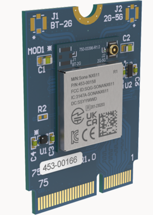
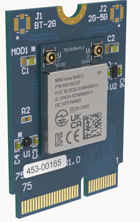
The SONA™NX611 series wireless modules include several product SKUs with different form factor, integration levels and RF paths. Please contact Ezurio Sales/FAE for further information. Ordering information is listed below.
This datasheet is subject to change. Please contact Ezurio for further information.
| Part Number | Description |
|---|---|
| 453-00155R | Module, Sona NX611 SIP, 2 RF Trace Pin, Tape and Reel |
| 453-00155C | Module, Sona NX611 SIP, 2 RF Trace Pin, Cut Tape |
| 453-00156R | Module, Sona NX611 SIP, 1 RF Trace Pin, Tape and Reel |
| 453-00156C | Module, Sona NX611 SIP, 1 RF Trace Pin, Cut Tape |
| 453-00157R | Module, Sona NX611 M.2 1216, 2 MHF4, Tape and Reel |
| 453-00157C | Module, Sona NX611 M.2 1216, 2 MHF4, Cut Tape |
| 453-00158R | Module, Sona NX611 M.2 1216, 1 MHF4, Tape and Reel |
| 453-00158C | Module, Sona NX611 M.2 1216, 1 MHF4, Cut Tape |
| 453-00165 | Module, Sona NX611 M.2 2230, 2 MHF4 |
| 453-00166 | Module, Sona NX611 M.2 2230, 1 MHF4 |
| 453-00155-K1 | Development Kit, Module, Sona NX611 SIP, 2 RF Trace Pin |
| 453-00156-K1 | Development Kit, Module, Sona NX611 SIP, 1 RF Trace Pin |
| 453-00165-K1 | Development Kit, Module, Sona NX611 M.2 2230, 2 MHF4 |
| 453-00166-K1 | Development Kit, Module, Sona NX611 M.2 2230, 1 MHF4 |
Features & Benefits
The Sona NX611 device features and benefits are described in the following table.
| Feature | Description |
|---|---|
| Key Wi-Fi Features |
|
| Key Bluetooth Features |
|
Specification Summary
Processor / SoC / Chipset
| Wireless | NXP NX611 or NX612 |
Wi-Fi
| Standards |
| ||||||||||||||||||||||||||||||||||||||||||||||||||||||||||||||||||||||||||||||||||||||||||||||||||||||||||||
| Interface | SDIO 3.0 (4-bit SDIO and 1-bit SDIO) with transfer rates up to SDR104 (208 MHz) | ||||||||||||||||||||||||||||||||||||||||||||||||||||||||||||||||||||||||||||||||||||||||||||||||||||||||||||
| Frequency Range | 5 GHz and 2.4 GHz Wi-Fi band operation | ||||||||||||||||||||||||||||||||||||||||||||||||||||||||||||||||||||||||||||||||||||||||||||||||||||||||||||
| Channel Support | 2.4 GHz:
5 GHz:
RF Channel Conversion Values - 2.4 GHz Channels
RF Channel Conversion Values - 5 GHz Channels
| ||||||||||||||||||||||||||||||||||||||||||||||||||||||||||||||||||||||||||||||||||||||||||||||||||||||||||||
| Wi-Fi Encryption |
| ||||||||||||||||||||||||||||||||||||||||||||||||||||||||||||||||||||||||||||||||||||||||||||||||||||||||||||
| Wi-Fi MAC |
| ||||||||||||||||||||||||||||||||||||||||||||||||||||||||||||||||||||||||||||||||||||||||||||||||||||||||||||
| Wi-Fi Baseband |
| ||||||||||||||||||||||||||||||||||||||||||||||||||||||||||||||||||||||||||||||||||||||||||||||||||||||||||||
| Power | Integrated PA, LNA | ||||||||||||||||||||||||||||||||||||||||||||||||||||||||||||||||||||||||||||||||||||||||||||||||||||||||||||
| Transmit Beamforming |
| ||||||||||||||||||||||||||||||||||||||||||||||||||||||||||||||||||||||||||||||||||||||||||||||||||||||||||||
| Coexistence |
|
Bluetooth
| Bluetooth Features |
|
| Bluetooth LE Features |
|
| Interface | Host Controller Interface (HCI) using high speed UART with support up to 3 Mbps baud rate |
Radio Performance
| 2.4 GHz Frequency Bands |
|
| 5 GHz Frequency Bands | EU:
FCC:
ISED:
MIC:
RCM:
|
| 6 GHz Frequency Bands | Complete / remove as needed |
Interfaces
| Physical Interfaces |
|
| Network Interfaces | Wi-Fi: SDIO 3.0 (4-bit SDIO and 1-bit SDIO) with transfer rates up to SDR104 (208 MHz) Bluetooth: Host Controller Interface (HCI) using high speed UART with support up to 3 Mbps baud rate |
| Memory Interfaces | One Time Programmable (OTP) memory to store the MAC address and calibration data |
| Audio Interfaces | Digital Audio:
|
Power
| Input Voltage | SIP- 76-pin LGA package:
1216- 96-pin LGA:
2230 Key E package:
|
| Power Management |
|
| I/O Signal Voltage | Set to 3.3V or 1.8V, by the power domains connected to VIO and VIO_SD |
Mechanical
| Dimensions | SIP- 76-pin LGA package:
1216- 96-pin LGA:
2230 Key E package:
|
| Weight | SIP- 76-pin LGA package:
1216- 96-pin LGA:
2230 Key E package:
|
Software
| OS Support | Linux Android |
| Security | Hardware root of trust Authenticated and secured boot. OTP-based life-cycle state support |
Environmental
| Operating Temperature | Operating temperature: -40 to 85°C |
| Storage Temperature | Storage temperature: -55 to 125°C |
| Operating Humidity | Less than 85% RH (non-condensing) |
| Storage Humidity | Less than 60% RH (non-condensing) |
| MSL (Moisture Sensitivity Level) | MSL4 (SIP), MSL1 (M2) |
| Maximum Electrostatic Discharge | Conductive 4KV; Air coupled 8KV (follow EN61000-4-2) |
| Lead Free | Lead-free and RoHS Compliant |
Certifications
| Regulatory Compliance |
|
| Compliance Standards | EU
FCC
ISED Canada
AS/NZS
|
| Bluetooth SIG | Bluetooth® SIG Qualification |
Development
| Development Kit |
|
Warranty
| Warranty Terms | One Year Warranty |
Functional Descriptions
Bluetooth Functional Description
I2S/PCM Interface Signals
| Pin Name | Type | Description | GPIO |
|---|---|---|---|
| PCM_DOUT / I2S_DOUT | O | PCM/I2S data out | GPIO[5] |
| PCM_DIN / I2S_DIN | I | PCM/I2S data in | GPIO[6] |
| PCM_CLK / I2S_BLCK | I/O | PCM/I2S clock, can be output (if central) or input (if peripheral) | GPIO[4] |
| PCM_SYNC / I2S_LRCLK | I/O | PCM/I2S sync, can be output (if central) or input (if peripheral) | GPIO[7] |
| PCM_MCLK / I2S_CCLK | O | Optional clock pins | GPIO[3] |
Clock frequency and audio data resolutions
Audio data may arrive with different input data formats with different sampling rates.
In master mode, the I2S interface uses an audio input clock of 4.096 MHz or 2.048 MHz to provide the appropriate M clock (MCLK) and bit clock (I2S_BCLK) frequency to match the sampling rates of each audio data format. The sampling rates can be 8 kHz to 16 kHz.
In slave mode, the I2S interface does not provide the bit clock (I2S_BCLK) but it can provide the M clock (MCLK).
Hardware Architecture
Block Diagrams
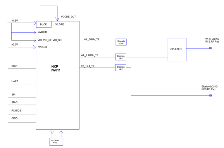
Sona NX611 SIP- 2 RF Trace Pin
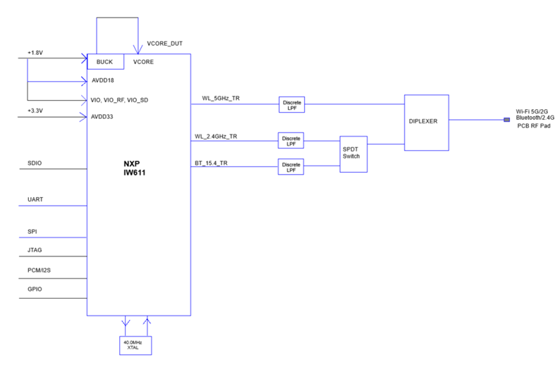
Sona NX611 SIP- 1 RF Trace Pin
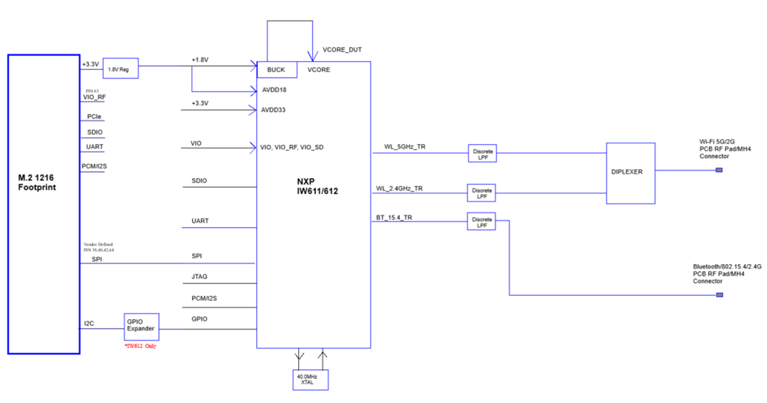
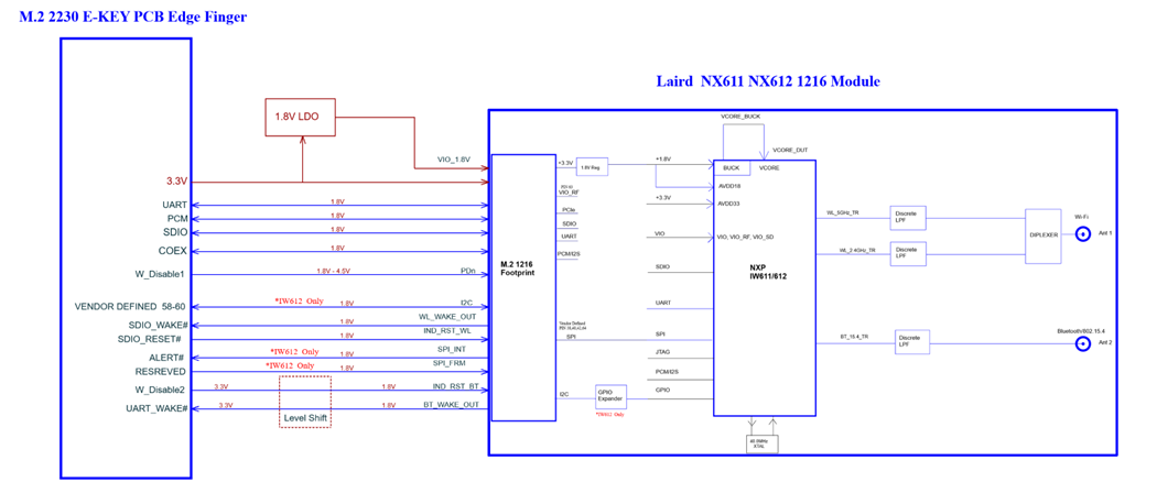
Sona NX611 1216 - 2 Trace Pin/MH4 Connector
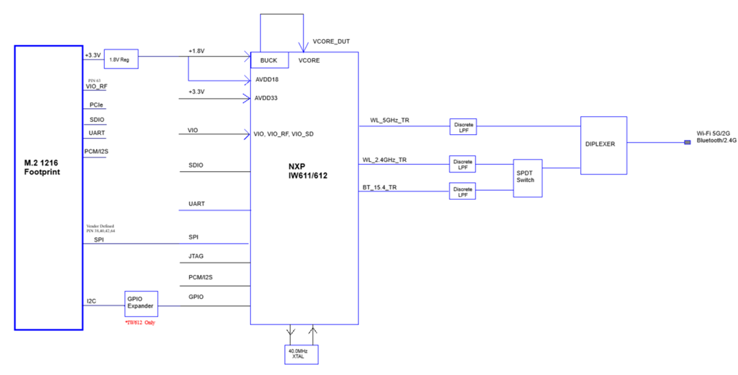
Sona NX611 1216- 1 RF Trace Pin/MH4 Connector
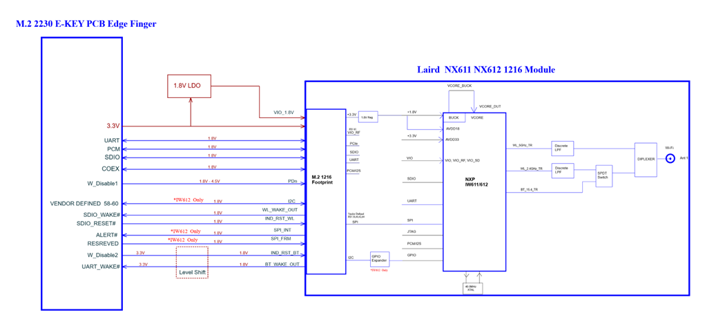
Sona NX611 M.2 2230- 2 MH4 Connector
Sona NX611 M.2 2230- 1 MH4
Pin-Out
The pin states information provided in the tables includes:
- No Pad Power State indicates the state when there is no power
- PwrDwn State denotes the power-down state in default configuration. Many pads have programmable power down values, which can be set by firmware.
- Reset State is the state after the power-on-reset state and before the hardware state (HW State)
- HW State (hardware state) is the state after boot code finishes and before firmware download begins (firmware may change the pin state). HW State may differ based on the pin muxing/strap setting. For example, for UART_RTSn and UART_SOUT, the boot code will enable the UART interface when the device is in SDIO-UARTmode, making the HW states output high and output low, respectively.
- PwrDwn Prog indicates if the power-down state can be programmed
Internal PU/PD columns indicates the following (the internal pull-up or pull-down applies when the pin is in input mode):
- Type of PU/PD (weak vs nominal)
- The polarity (PU vs. PD)
- PU denotes whether the pull-up can be programmed or not
- PD denotes whether the pull-down can be programmed or not
- Pull-up and pull-down are only effective when the pad is in input mode
After firmware is downloaded, the pads (GPIO, RF control, and so on) are programmed in functional mode per the functionality of the pins
- Internal weak pull-up resistance 800kΩ
- Internal nominal pull-up resistance 100kΩ
- All pins No Pad power state are tristate
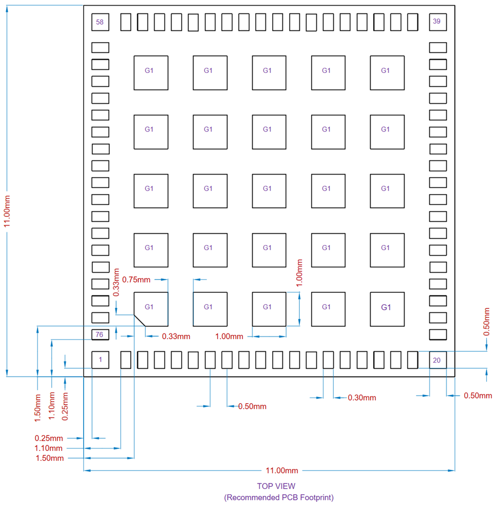
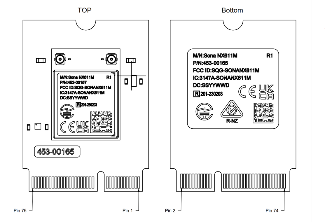
NX611 SiP Pinout
| Pin # | Pin Name | Description | Supply Domain | Reset State | HW State | PwrDwn state | PwrDwn prog. | Internal PU/PD | PU | PD | Comment |
|---|---|---|---|---|---|---|---|---|---|---|---|
| 1 | GND | Ground | - | - | - | - | - | - | - | - | |
| 2 | VIO_SD | SDIO Logic Level | VIO_SD | - | - | - | - | - | - | - | 1.8V required for SDR data rates |
| 3 | GND | Ground | - | - | - | - | - | - | - | - | |
| 4 | SD_CMD | SD CMD (input/output) | VIO_SD | Input | Input | Tristate | No | Nominal PU | Yes | Yes | |
| 5 | SD_CLK | SD Clock input | VIO_SD | Input | Input | Tristate | No | Nominal PU | Yes | Yes | |
| 6 | SD_DAT[1] | SD Data line bit[1] | VIO_SD | Input | Input | Tristate | No | Nominal PU | Yes | Yes | |
| 7 | SD_DAT[3] | SD Data line bit[3] | VIO_SD | Input | Input | Tristate | No | Nominal PU | Yes | Yes | |
| 8 | GND | Ground | - | - | - | - | - | - | - | - | |
| 9 | SD_DAT[2] | SD Data line bit[2] | VIO_SD | Input | Input | Tristate | No | Nominal PU | Yes | Yes | |
| 10 | SD_DAT[0] | SD Data line bit[0] | VIO_SD | Input | Input | Tristate | No | Nominal PU | Yes | Yes | |
| 11 | GPIO[21]/ SD_INT | SDIO interrupt signal (output). | VIO | Output high | Output low | Drive low | Yes | Nominal PU | Yes | Yes | |
| 12 | BUCK_SENSE | Internal buck voltage | - | - | - | - | - | - | - | - | Do not connect. For troubleshooting only. |
| 13 | VIO | 1.8V/3.3V digital I/O power supply | - | - | - | - | - | - | - | - | Sets Logic Levels for GPIO and Control Lines |
| 14 | GPIO[8]/ UART_CTS | UART clear-to-send input signal (active low) | VIO | Input | Input | Tristate | Yes | Weak PU | Yes | Yes | |
| 15 | GPIO[10]/ UART_RX | UART serial input signal. | VIO | Input | Input | Tristate | Yes | Nominal PU | Yes | Yes | |
| 16 | GPIO[9]/ UART_RTS | UART request-to-send output signal (active low). | VIO | Output high | Output high | Drive high | Yes | Nominal PU | Yes | Yes | |
| 17 | GPIO[11]/ UART_TX | UART serial output signal. | VIO | Output high | Output high | Drive low | Yes | Nominal PU | Yes | Yes | |
| 18 | GPIO[13]/ EXT_REQ | External radio request input signal (COEX) | VIO | Input | Input | Drive high | Yes | Nominal PU | Yes | Yes | |
| 19 | GPIO[12]/ EXT_STATE | External radio state input signal (COEX) | VIO | Input | Input | Tristate | Yes | Weak PU | Yes | Yes | |
| 20 | GND | Ground | - | - | - | - | - | - | - | - | |
| 21 | GPIO[14]/ EXT_GNT | External radio grant output signal (COEX) | VIO | Input | Input | Tristate | Yes | Nominal PU | Yes | Yes | |
| 22 | GPIO[15]/EXT_PRI | External radio input priority signal (COEX) | VIO | Output low | Output low | Drive low | Yes | Nominal PU | Yes | Yes | |
| 23 | GPIO[0]/XOSC_EN | Oscillator enable (output) | VIO | Output | Output high | Drive low | Yes | Nominal PU | Yes | Yes | May be used as an additional GPIO. |
| 24 | GPIO[20]/EXT_FREQ | External radio frequency input signal (COEX) | VIO | Input | Input | Drive low | Yes | Nominal PU | Yes | Yes | |
| 25 | CONFIG_ HOST[1] | NC | AVDD18 | Input | Input | Tristate | No | Weak PU | Yes | Yes | Do not connect. |
| 26 | CONFIG _HOST[0] | NC | AVDD18 | Input | Input | Tristate | No | Weak PU | Yes | Yes | Do not connect. |
| 27 | GND | Ground | - | - | - | - | - | - | - | - | - |
| 28 | GPIO[4]/ PCM_CLK | PCM data clock | VIO | Input | Input | Tristate | Yes | Weak PU | Yes | Yes | Output if master, input if slave |
| 29 | GPIO[3]/ PCM_MCLK | PCM clock output (optional) | VIO | Input | Input | Tristate | Yes | Nominal PU | Yes | Yes | |
| 30 | GPIO[5]/ PCM_DOUT | PCM transmit data(output) | VIO | Input | Input | Tristate | Yes | Weak PU | Yes | Yes | |
| 31 | GPIO[6]/ PCM_DIN | PCM receive data(input) | VIO | Input | Input | Tristate | Yes | Weak PU | Yes | Yes | |
| 32 | GPIO[7]/ PCM_SYNC | PCM frame sync | VIO | Input | Input | Tristate | Yes | Nominal PU | Yes | Yes | Output if master, input if slave |
| 33 | GPIO[2]/ IND_RST_BT | Independent software reset Bluetooth (input) | VIO | Input | Input | Tristate | Yes | Nominal PU | Yes | Yes | |
| 34 | GPIO[1]/ IND_RST_WL | Independent software reset Wi-Fi (input) | VIO | Input | Input | Tristate | Yes | Nominal PU | Yes | Yes | |
| 35 | GND | Ground | - | - | - | - | - | - | - | - | |
| 36 | AVDD18 | 1.8V analog supply | - | - | - | - | - | - | - | - | |
| 37 | AVDD18 | 1.8V analog supply | - | - | - | - | - | - | - | - | |
| 38 | GND | Ground | - | - | - | - | - | - | - | - | - |
| 39 | GND | Ground | - | - | - | - | - | - | - | - | - |
| 40 | PDn | Full Power-down (input) 0 = full power-down mode 1 = normal mode
| VIO | - | - | - | - | Weak PD | - | - | Module has a 51K Ω Pull Up to 3.3V. For increased noise and ESD immunity, connect to host output pin. |
| 41 | GND | Ground | - | - | - | - | - | - | - | - | - |
| 42 | GND | Ground | - | - | - | - | - | - | - | - | - |
| 43 | GND | Ground | - | ||||||||
| 44 | RF_TR_5 |
| AVDD18 | ||||||||
| 45 | GND | Ground | - | - | - | - | - | - | - | - | - |
| 46 | AVDD33 | 3.3V analog supply | - | - | - | - | - | - | - | - | - |
| 47 | AVDD33 | 3.3V analog supply | - | - | - | - | - | - | - | - | - |
| 48 | GND | Ground | - | - | - | - | - | - | - | - | - |
| 49 | GND | Ground | - | - | - | - | - | - | - | - | - |
| 50 | GND | Ground | - | - | - | - | - | - | - | - | - |
| 51 | GND | Ground | - | - | - | - | - | - | - | - | - |
| 52 | BRF_ANT |
| AVDD18 | - | - | - | - | - | - | - | |
| 53 | GND | Ground | - | - | - | - | - | - | - | - | - |
| 54 | GND | Ground | - | - | - | - | - | - | - | - | - |
| 55 | GND | Ground | - | - | - | - | - | - | - | - | - |
| 56 | GPIO[26]/ WCI_SOUT | Receive signal from external radio (input) (COEX) | VIO | Input | Input | Drive low | Yes | Nominal PU | Yes | Yes | |
| 57 | GPIO[25]/ WCI-2_SIN | Transmit signal to external radio (output) (COEX) | VIO | Input | Input | Tristate | Yes | Nominal PU | Yes | Yes | |
| 58 | GND | Ground | - | - | - | - | - | - | - | - | - |
| 59 | RF_CNTL4 | RF control line 4 | AVDD33 | ||||||||
| 60 | RF_CNTL3 | RF control line 3 | AVDD33 | Input | Input | Drive high | Yes | Weak PU | No | No | |
| 61 | RF_CNTL2 | RF control line 2 | AVDD33 | Output low | Output low | Drive low | Yes | Nominal PU | No | No | |
| 62 | RF_CNTL1 | RF control line 1 | AVDD33 | Output high | Output high | Drive high | Yes | Weak PU | No | No | |
| 63 | RF_CNTL0 | RF control line 0 | AVDD33 | Output low | Output low | Drive low | Yes | Nominal PU | No | No | |
| 64 | GPIO[18]/ BT_WAKE_IN | Bluetooth wake-up signal (Input) | VIO | Input | Input | Tristate | Yes | Weak PU | Yes | Yes | |
| 65 | GPIO[19]/ BT_WAKE_OUT | Bluetooth wake-up signal (output) | VIO | Input | Input | Drive low | Yes | Nominal PU | Yes | Yes | |
| 66 | GPIO[17]/ WL_WAKE_OUT | Wi-Fi radio wake-up signal (output) | VIO | Input | Input | Drive low | Yes | Nominal PU | Yes | Yes | |
| 67 | GPIO[16]/WL_WAKE_IN | Wi-Fi radio wake-up signal (input) | VIO | Input | Input | Tristate | Yes | Weak PU | Yes | Yes | |
| 68 | GND | Ground | - | - | - | - | - | - | - | - | - |
| 69 | GPIO[22] | I/O | VIO | Output high | Output low | Tristate | Yes | Nominal PU | Yes | Yes | |
| 70 | GPIO[23] | I/O | VIO | Input | Input | Tristate | Yes | Nominal PU | Yes | Yes | |
| 71 | GPIO[24] | I/O | VIO | Output low | Output high | Tristate | Yes | Weak PU | Yes | Yes | |
| 72 | GPIO[27] | I/O | VIO | Input | Input | Tristate | Yes | Weak PU | Yes | Yes | |
| 73 | GPIO[29]/ JTAG_TMS | JTAG controller select (input) | VIO | Input | Input | Tristate | Yes | Nominal PU | Yes | Yes | |
| 74 | GPIO[31]/ JTAG_TDO | JTAG test data signal (output) | VIO | Input | Input | Tristate | Yes | Weak PU | Yes | Yes | |
| 75 | GPIO[28]/ JTAG_TCK | JTAG test clock signal (input) | VIO | Input | Input | Tristate | Yes | Nominal PU | Yes | Yes | |
| 76 | GPIO[30]/ JTAG_TDI | JTAG test data signal (input) | VIO | Input | Input | Tristate | Yes | Nominal PU | Yes | Yes | |
| G1 | GND | Ground | - | - | - | - | - | - | - | - | - |
NX611 M.2 1216 Pinout
Notes:
Pins may be Multi-Functional Pins (MFP).
All GPIO can be programmed with PU or PD
| Pin # | NX611 Pin Name | Description | Supply Domain | Reset State | HW State | PwrDwn State | PwrDwnProg | Internal PU/PD | Comment |
|---|---|---|---|---|---|---|---|---|---|
| 1 | UIM_POWER_ SRC/ GPIO1 | Not Used | - | - | - | - | - | - | NO CONNECTION |
| 2 | UIM_POWER_ SNK | Not Used | - | - | - | - | - | - | NO CONNECTION |
| 3 | UIM_SWP | Not Used | - | - | - | - | - | - | NO CONNECTION |
| 4 | 3.3V | 3.3V Supply | - | - | - | - | - | - | |
| 5 | 3.3V | 3.3V Supply | - | - | - | - | - | - | |
| 6 | GND | Module Ground | - | - | - | - | - | - | |
| 7 | RESERVED | Not Used | - | NO CONNECTION | |||||
| 8 | ALERT# | Not Used | - | - | - | - | - | - | NO CONNECTION |
| 9 | I2C_CLK | Not Used | - | - | - | - | - | - | NO CONNECTION |
| 10 | I2C_DATA | Not Used | - | - | - | - | - | - | NO CONNECTION |
| 11 | COEX_RXD | GPIO25/WCI-2_SIN MFP -WCI-2 coexistence serial interface input | VIO | Input | Input | Tristate | Yes | Nominal PU | |
| 12 | COEX_TXD | GPIO26/WCI-2_SOUT MFP -WCI-2 coexistence serial interface output | VIO | Input | Input | Drive low | Yes | Nominal PU | |
| 13 | COEX3 | Not Used | - | - | - | - | - | - | NO CONNECTION |
| 14 | SYSCLK/ GNSS_0 | Not Used | - | - | - | - | - | - | NO CONNECTION |
| 15 | TX_BLANKING/ GNSS_1 | Not Used | - | - | - | - | - | - | NO CONNECTION |
| 16 | RESERVED | Not Used | - | - | - | - | - | - | NO CONNECTION |
| 17 | GND | Module Ground | - | - | - | - | - | - | |
| 18 | RESERVED | Not Used | - | - | - | - | - | - | NO CONNECTION |
| 19 | RESERVED | GPIO13 | VIO | Input | Input | Drive high | Yes | Nominal PU | Can be used as GPIO. No connect if unused |
| 20 | GND | Module Ground | - | - | - | - | - | ||
| 21 | PETn1 | Not Used | - | - | - | - | - | - | NO CONNECTION |
| 22 | PETp1 | Not Used | - | - | - | - | - | - | NO CONNECTION |
| 23 | GND | Module Ground | - | - | - | - | - | - | |
| 24 | PERn1 | Not Used | - | - | - | - | - | - | NO CONNECTION |
| 25 | PERp1 | Not Used | - | - | - | - | - | - | NO CONNECTION |
| 26 | GND | Module Ground | - | - | - | - | - | - | |
| 27 | SUSCLK(32kHz) | Not Used | - | - | - | - | - | - | NO CONNECTION |
| 28 | W_DISABLE1# | PDn Full Power-down (input) 0 = full power-down mode 1 = normal mode
| 1.8V | Module has a weak 51K Ω Pull Up. For increased noise and ESD immunity, connect to host output pin. | |||||
| 29 | PEWAKE# | Not Used | - | - | - | - | - | - | NO CONNECTION |
| 30 | CLKREQ# | Not Used | - | - | - | - | - | - | NO CONNECTION |
| 31 | PERST# | Not Used | - | - | - | - | - | - | NO CONNECTION |
| 32 | GND | Module Ground | - | - | - | - | - | - | |
| 33 | REFCLKn0 | Not Used | - | - | - | - | - | - | NO CONNECTION |
| 34 | REFCLKp0 | Not Used | - | - | - | - | - | - | NO CONNECTION |
| 35 | GND | Module Ground | - | - | - | - | - | - | |
| 36 | PETn0 | Not Used | - | - | - | - | - | - | NO CONNECTION |
| 37 | PETp0 | Not Used | - | - | - | - | - | - | NO CONNECTION |
| 38 | GND | Module Ground | - | - | - | - | - | - | |
| 39 | PERn0 | Not Used | - | - | - | - | - | - | NO CONNECTION |
| 40 | PERp0 | Not Used | - | - | - | - | - | - | NO CONNECTION |
| 41 | GND | Module Ground | - | - | - | - | - | - | |
| 42 | VENDOR DEFINED | GPIO15 | VIO | Output low | Output low | Drive low | Yes | Nominal PU | Can be used as GPIO. No connect if unused |
| 43 | VENDOR DEFINED | GPIO18/BT_WAKE_IN MFP -Bluetooth radio wake-up (input) | VIO | Output low | Output low | Drive low | Yes | Nominal PU | |
| 44 | VENDOR DEFINED | GPIO16/WL_WAKE_IN MFP -WiFI radio wake-up (input) | VIO | Input | Input | Tristate | Yes | Weak PU | |
| 45 | SDIO RESET# | GPIO1/IND_RST_WL MFP -Independent software reset for Wi-Fi (input) | VIO | Input | Input | Tristate | Yes | Nominal PU | |
| 46 | SDIO WAKE# | GPIO17/WL_WAKE_OUT Wi-Fi radio to host wake-up (output) | VIO | Input | Input | Drive low | Yes | Nominal PU | |
| 47 | SDIO DATA3 | SDIO DATA3 | VIO | Input | Input | Tristate | No | Nominal PU | |
| 48 | SDIO DATA2 | SDIO DATA2 | VIO | Input | Input | Tristate | No | Nominal PU | |
| 49 | SDIO DATA1 | SDIO DATA1 | VIO | Input | Input | Tristate | No | Nominal PU | |
| 50 | SDIO DATA0 | SDIO DATA0 | VIO | Input | Input | Tristate | No | Nominal PU | |
| 51 | SDIO CMD | SDIO CMD | VIO | Input | Input | Tristate | No | Nominal PU | Input |
| 52 | SDIO CLK | SDIO CLK | VIO | Input | Input | Tristate | No | Nominal PU | |
| 53 | UART WAKE# | GPIO19/BT_WAKE_OUT# MFP -Bluetooth to host wake-up (output) | VIO | Input | Input | Drive low | Yes | Nominal PU | |
| 54 | UART CTS | GPIO8/UART_CTS MFP UART clear to send input (active low) | VIO | Input | Input | Tristate | Yes | Weak PU | |
| 55 | UART Tx | GPIO11/UART_TX MFP UART TX output | VIO | Output high | Output high | Drive low | Yes | Nominal PU | |
| 56 | UART Rx | GPIO10/UART_RX MFP UART RX input | VIO | Input | Input | Tristate | Yes | Nominal PU | |
| 57 | UART RTS | GPIO9/UART_RTS MFP UART request to send output (active low) | VIO | Output high | Output high | Drive high | Yes | Nominal PU | |
| 58 | PCM_SYNC/I2S_WS | GPIO7/PCM_SYNC MFP -PCM frame sync -I2S left/right clock | VIO | Input | Input | Tristate | Yes | Nominal PU | |
| 59 | PCM_IN/I2S_SD_IN | GPIO6/PCM_DIN MFP PCM/I2S receive data signal (input) | VIO | Input | Input | Tristate | Yes | Weak PU | |
| 60 | PCM_OUT/I2S_ SD_OUT | GPIO5/PCM_DOUT MFP PCM/I2S transmit data (output) | VIO | Input | Input | Tristate | Yes | Weak PU | |
| 61 | PCM_CLK/I2S_ SCK | GPIO4/PCM_CLK MFP
-I2S_BCLK - I2S bit clock | VIO | Input | Input | Tristate | Yes | Weak PU | |
| 62 | GND | Module Ground | - | ||||||
| 63 | W_DISABLE2# | GPIO2/IND_RST_BT# MFP -Independent software reset for Bluetooth | VIO | Input | Input | Tristate | Yes | Nominal PU | |
| 64 | LED_2# | Not Used | - | - | - | - | NO CONNECTION | ||
| 65 | LED_1# | Not Used | - | - | - | - | NO CONNECTION | ||
| 66 | RESERVED/ VIO_1.8 | GPIO Voltage Sets logic level for all GPIo, UART and SDIO | 1.8V or 3.3V | - | - | - | 1.8V required for extended SDIO Data rates | ||
| 67 | RESERVED | Not Used | - | - | - | - | NO CONNECTION | ||
| 68 | GND | Module Ground | - | - | - | - | |||
| 69 | USB_D- | Not Used | - | - | - | - | NO CONNECTION | ||
| 70 | USB_D+ | Not Used | - | - | - | - | NO CONNECTION | ||
| 71 | GND | Module Ground | - | - | - | - | |||
| 72 | 3.3V | 3.3V Supply | - | - | - | - | |||
| 73 | 3.3V | 3.3V Supply | - | - | - | - | |||
| 74 | GND | Module Ground | - | - | - | - | |||
| 75 | GND | Module Ground | - | - | - | - | |||
| 76 | GND/VIO_CFG | Not Used | - | - | - | - | NO CONNECTION | ||
| 77 | GND | Module Ground | - | - | - | - | |||
| 78 | GND | Module Ground | - | - | - | - | |||
| 79 | GND | Module Ground | - | - | - | - | |||
| 80 | GND | Module Ground | - | - | - | - | |||
| 81 | WL_C2 | Not Used | - | - | - | - | NO CONNECTION | ||
| 82 | GND | Module Ground | - | - | - | - | |||
| 83 | GND | Module Ground | - | - | - | - | |||
| 84 | GND | Module Ground | - | - | - | - | |||
| 85 | GND | Module Ground | - | - | - | - | |||
| 86 | WL_C0 | Not Used | - | - | - | - | NO CONNECTION | ||
| 87 | GND | Module Ground | - | - | - | - | |||
| 88 | GND | Module Ground | - | - | - | - | |||
| 89 | GND | Module Ground | - | - | - | - | |||
| 90 | GND | Module Ground | - | - | - | - | |||
| 91 | GND | Module Ground | - | - | - | - | |||
| 92 | WL_C1 | Not Used | - | - | - | - | NO CONNECTION | ||
| 93 | GND | Module Ground | - | - | - | - | |||
| 94 | GND | Module Ground | - | - | - | - | |||
| 95 | GND | Module Ground | - | - | - | - | |||
| 96 | GND | Module Ground | - | - | - | - | |||
| G1 | GND | Module Ground | - | - | - | - |
NX611 M.2 2230 Key E Pinout
Notes:
Pins may be Multi-Functional Pins (MFP).
All GPIO can be programmed with PU or PD
| Pin # | NX611 Pin Name | Description | Supply Domain | Reset State | HW State | PwrDwn State | PwrDwnProg | Internal PU/PD | Comment |
|---|---|---|---|---|---|---|---|---|---|
| 1 | GND | Module Ground | - | - | - | - | - | - | |
| 2 | 3.3 V | 3.3V Supply | - | - | - | - | - | - | |
| 3 | USB_D+ | Not Used | - | - | - | - | - | - | Do Not Connect |
| 4 | 3.3 V | 3.3V Supply | - | - | - | - | - | - | |
| 5 | USB_D- | Not Used | - | - | - | - | - | - | Do Not Connect |
| 6 | LED_1# (I)(OD) | Not Used | - | - | - | - | - | - | Do Not Connect |
| 7 | GND | Module Ground | - | - | - | - | - | - | |
| 8 | PCM_CLK/I2S_SCK (I/O)(0/1.8V) | GPIO4/PCM_CLK MFP
-I2S_BCLK - I2S bit clock | 1.8V | Input | Input | Tristate | Yes | Weak PU | |
| 9 | SDIO_CLK/SYSCLK (I) (0/1.8V) | SDIO_CLK | 1.8V | Input | Input | Tristate | No | Nominal PU | |
| 10 | PCM_SYNC/ I2S_WS (I/O)(0/1.8V) | GPIO7/PCM_SYNC MFP -PCM frame sync -I2S left/right clock | 1.8V | Input | Input | Tristate | Yes | Nominal PU | |
| 11 | SDIO_CMD (I/O) (0/1.8V) | SDIO_CMD | 1.8V | Input | Input | Tristate | No | Nominal PU | |
| 12 | PCM_OUT/I2S_SD_OUT (O)(0/1.8V) | GPIO5/PCM_DOUT PCM/I2S TXD (output) | 1.8V | Input | Input | Tristate | Yes | Weak PU | |
| 13 | SDIO_DATA0 (I/O) (0/1.8V) | SDIO_DATA0 | 1.8V | Input | Input | Tristate | No | Nominal PU | |
| 14 | PCM_IN/I2S_SD_IN (I)(0/1.8V) | GPIO6/PCM_DIN PCM/I2S RXD (input) | 1.8V | Input | Input | Tristate | Yes | Weak PU | |
| 15 | SDIO_DATA1 (I/O) (0/1.8V) | SDIO_DATA1 | 1.8V | Input | Input | Tristate | No | Nominal PU | |
| 16 | LED_2# (I)(OD) | Not Used | - | - | - | - | - | - | NO CONNECTION |
| 17 | SDIO_DATA2 (I/O) (0/1.8V) | SDIO_DATA2 | 1.8V | Input | Input | Tristate | No | Nominal PU | |
| 18 | GND/VIO_CFG | Module Ground | Ground | ||||||
| 19 | SDIO_DATA3 (I/O) (0/1.8V) | SDIO_DATA3 | 1.8V | Input | Input | Tristate | No | Nominal PU | |
| 20 | UART WAKE# (O)(0/3.3V) | GPIO19/BT_WAKE_OUT# Bluetooth to host wake-up (output) | 3.3V | Input | Input | Drive low | Yes | Nominal PU | |
| 21 | SDIO WAKE# (O)(0/1.8V) | GPIO17/WL_WAKE_OUT Wi-Fi radio to host wake-up (output) | 1.8V | Input | Input | Drive low | Yes | Nominal PU | |
| 22 | UART TXD (O)(0/1.8V) | GPIO11/UART_TX UART TX output | 1.8V | Output high | Output high | Drive low | Yes | Nominal PU | |
| 23 | SDIO RESET# (I)(0/1.8V) | GPIO1/IND_RST_WL Independent software reset for Wi-Fi (input) | 1.8V | Input | Input | Tristate | Yes | Nominal PU | |
| 24-31 | CONNECTOR KEY E | Not Used | - | - | - | - | - | No Pins. Used for Keying. | |
| 32 | UART_RXD (I)(0/1.8V) | GPIO10/UART_RX UART RX input | 1.8V | Input | Input | Tristate | Yes | Nominal PU | |
| 33 | GND | Module Ground | - | - | - | - | - | ||
| 34 | UART_RTS (O)(0/1.8V) | GPIO9/UART_RTS UART (output) | 1.8V | Output high | Output high | Drive high | Yes | Nominal PU | |
| 35 | PETp0 | Not Used | - | - | - | - | - | ||
| 36 | UART_CTS (I)(0/1.8V) | GPIO8/UART_CTS UART (input) | 1.8V | Input | Input | Tristate | Yes | Weak PU | |
| 37 | PERn0 | Not Used | - | - | - | - | - | NO CONNECTION | |
| 38 | VENDOR DEFINED | GPIO15 | 1.8V | Output low | Output low | Drive low | Yes | Nominal PU | Can be used as GPIO. No connect if unused |
| 39 | GND | Module Ground | |||||||
| 40 | VENDOR DEFINED | GPIO16/WL_WAKE_IN WiFI radio wake-up (input) | 1.8V | Input | Input | Tristate | Yes | Weak PU | |
| 41 | PETp0 | Not Used | - | - | - | - | - | NO CONNECTION | |
| 42 | VENDOR DEFINED | GPIO18/BT_WAKE_IN -Bluetooth radio wake-up (input) | 1.8V | Input | Input | Tristate | Yes | Weak PU | |
| 43 | PETn0 | Not Used | - | - | - | - | - | - | NO CONNECTION |
| 44 | COEX3 (I/O)(0/1.8V) | Not Used | - | - | - | - | - | - | NO CONNECTION |
| 45 | GND | Module Ground | - | - | - | - | - | - | |
| 46 | COEX_TXD (O)(0/1.8V) | GPIO26/WCI-2_SOUT -WCI-2 coexistence serial interface output | Input | Input | Drive low | Yes | Nominal PU | ||
| 47 | REFCLKp0 | Not Used | - | - | - | - | - | - | NO CONNECTION |
| 48 | COEX_RXD (I)(0/1.8V) | GPIO25/WCI-2_SIN -WCI-2 coexistence serial interface input | Input | Input | Tristate | Yes | Nominal PU | ||
| 49 | REFCLKn0 | Not Used | - | - | - | - | - | - | NO CONNECTION |
| 50 | SUSCLK (I)( 0/1.8V/3.3V) | Not Used | - | - | - | - | - | - | NO CONNECTION |
| 51 | GND | Module Ground | - | - | - | - | - | - | |
| 52 | PERST0# (I)( 0/1.8V/3.3V) | Not Used | - | - | - | - | - | - | NO CONNECTION |
| 53 | CLKREQ0# (I/O)( 0/1.8V/3.3V) | Not Used | - | - | - | - | - | - | NO CONNECTION |
| 54 | W_DISABLE2# (I)(0/3.3V) | GPIO2/IND_RST_BT# Independent software reset for Bluetooth | 3.3V | Input | Input | Tristate | Yes | Nominal PU | |
| 55 | PEWAKE0# (I/O)( 0/1.8V/3.3V) | Not Used | - | - | - | - | - | - | NO CONNECTION |
| 56 | W_DISABLE1# (I)(0/3.3V) | PDn Full Power-down (input) 0 = full power-down mode 1 = normal mode
| 1.8V | - | - | - | - | - | Module has a weak 51K Ω Pull Up. For increased noise and ESD immunity, connect to host output pin. |
| 57 | GND | Module Ground | - | - | - | - | |||
| 58 | I2C_DATA (I/O)(0/1.8 V) | Not Used | - | - | - | NO CONNECTION | |||
| 59 | RESERVED/PERp1 | Not Used | - | - | - | - | NO CONNECTION | ||
| 60 | I2C_CLK (O)(0/1.8 V) | Not Used | - | - | - | - | NO CONNECTION | ||
| 61 | RESERVED/PERn1 | Not Used | - | - | - | - | NO CONNECTION | ||
| 62 | ALERT# (I)(0/1.8 V) | Not Used | - | - | - | - | NO CONNECTION | ||
| 63 | GND | Module Ground | - | - | - | - | |||
| 64 | RESERVED/VIO 1.8V | Not Used | - | - | - | - | |||
| 65 | RESERVED/PETp1 | Not Used | - | - | - | - | NO CONNECTION | ||
| 66 | UIM_SWP/PERST1# | Not Used | - | - | - | - | NO CONNECTION | ||
| 67 | RESERVED/PETn1 | Not Used | - | - | - | - | NO CONNECTION | ||
| 68 | UIM_POWER_SNK/CLKREQ1# | Not Used | - | - | - | - | NO CONNECTION | ||
| 69 | GND | Module Ground | - | - | - | - | |||
| 70 | UIM_POWER_SRC/GPIO_1/PEWAKE1# | Not Used | - | - | - | - | NO CONNECTION | ||
| 71 | RESERVED | Not Used | - | - | - | - | NO CONNECTION | ||
| 72 | 3.3 V | 3.3V Supply | - | - | - | - | |||
| 73 | RESERVED | Not Used | - | - | - | - | NO CONNECTION | ||
| 74 | 3.3 V | 3.3V Supply | - | - | - | - | |||
| 75 | GND | Module Ground | - | - | - | - |
Mechanical Drawings
NX611 SIP Module
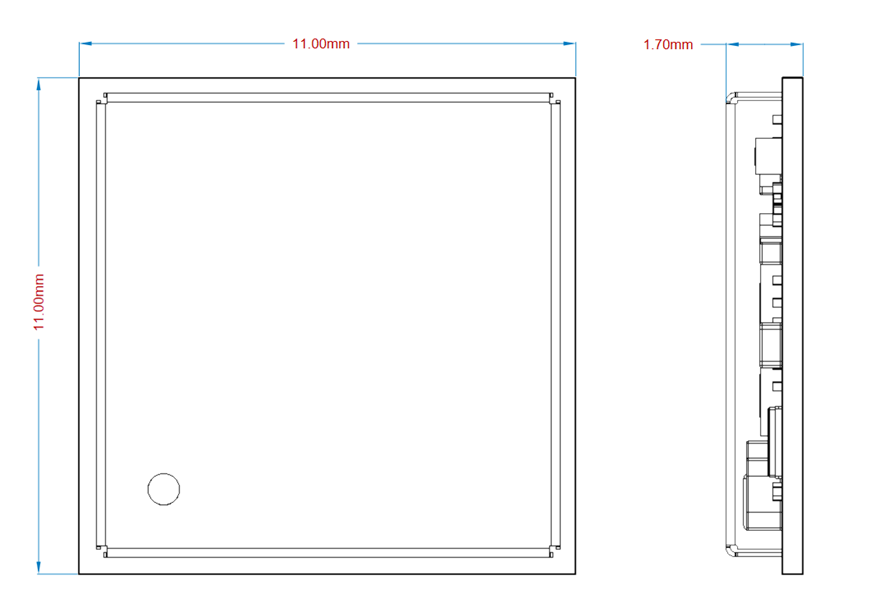
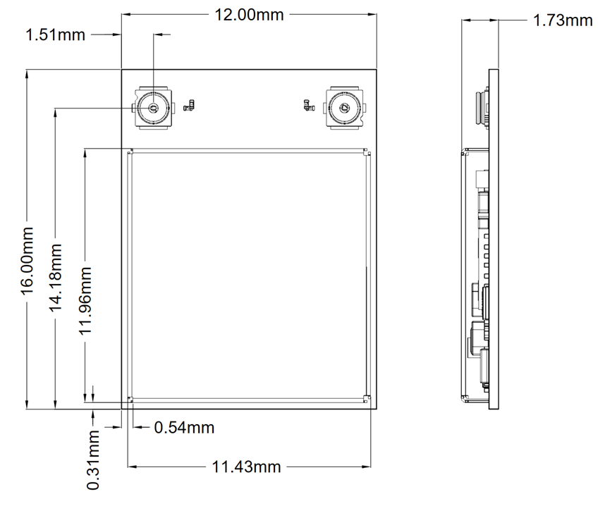
NX611 1216 Module
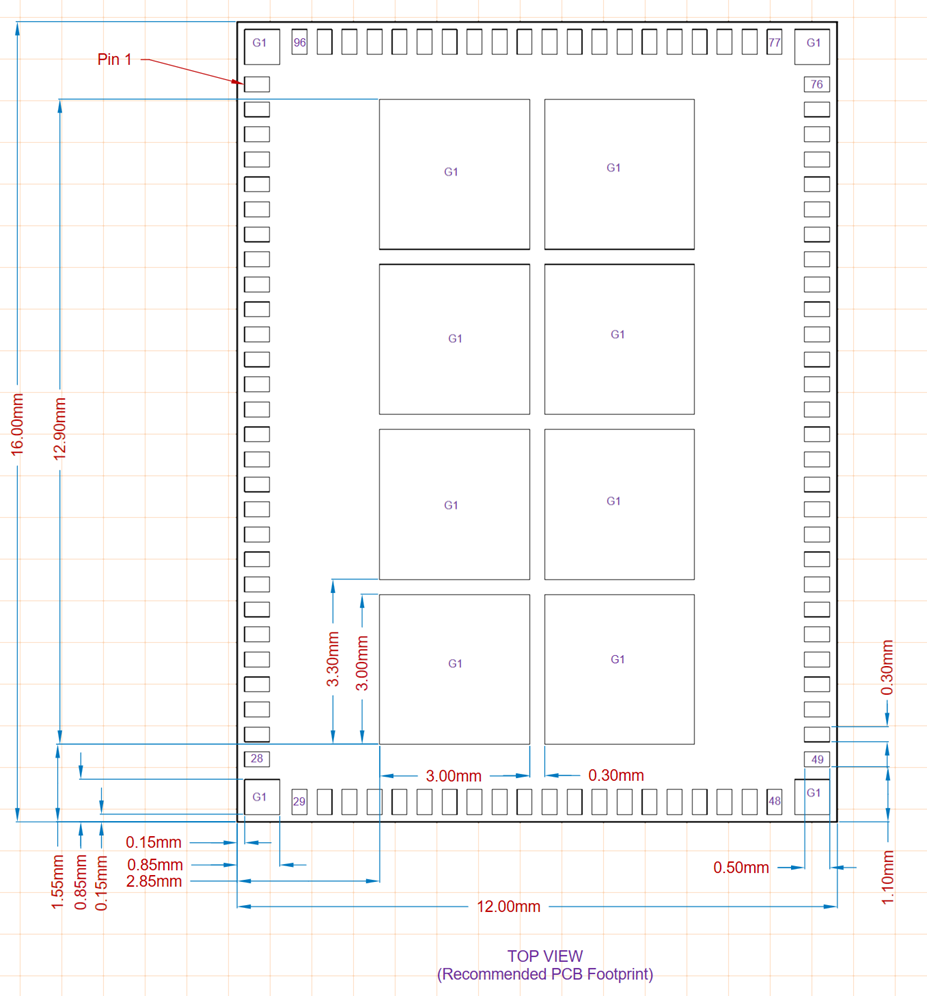
NX611 M.2 2230 Key-E Module
M.2 2230 Key-E Mounting
The Sona NX611 M.2 2230 Module connects to the host via a standard PCI EXPRESS M2 connector.
Mounting Connectors and Standoffs
| M.2 Key-E Connector | Connector Height | Stand-off |
|---|---|---|
| KYOCERA 24-6411-067-101-894E | 2.3 mm | EMI STOP F50M16-041525P1D4M |
| AMP MDT420E01001 | 2.5 mm | Alink, N0254020A |
| JAE SM3ZS067U310AERxxxx | 3.1 mm | JAE SM3ZS067U310-NUT1-Rxxxx |
Host Interface Specifications
Power Supplies
Power-up sequence
The Sona NX611 does not have power-up sequence requirements. The power-down pin (PDn) must be held low (asserted) until all external clock and power supply rails are stable.
PDn held low (asserted)
Power-down
The Sona NX611 modules can enter the lowest power mode when Wi-Fi and Bluetooth are inactive. To achieve this, you can assert the PDn (Power Down) pin low, which puts the module into power-down mode. The same power-down state can be achieved by powering off 3V3, 1V8, VIO_GPIO and VIO_SD.
After PDn is deasserted (high), the device takes 20 ms to get ready for SDIO enumeration.
Note: Firmware download is required again after exiting power-down mode.
PDn Pin (Power Down Timing)-Power remains high at PDn assertion
PDn Pin (Power Down Timing)-Power remains high at PDn assertion
| Symbol | Parameter | Condition | Min. | Typ. | Max. | Unit |
|---|---|---|---|---|---|---|
| tPU_RESET | Valid power to PDn deasserted | - | 0 | -- | -- | mS |
| tRPW | PDn pulse width | - | 1 | -- | -- | μs |
| tINIT | From PDn de-assertion to device ready (SDIO bus enumeration) | - | 20 | -- | -- | mS |
| VIH | Output high voltage | - | 1.4 | -- | 4.5 | V |
| VIL | Output low voltage | - | -0.4 | -- | 0.5 | V |
Wake-up/Interrupt Pins
Deep sleep mode is used to reduce power consumption. Optional wake up input pins are used to wake up the Sona NX611 from sleep. Optional wake up output pins can be used to wake up a host or signal a host that WiFi or Bluetooth data is available.
Wake-up/interrupt pins (MFP)
| Pin name | I/O type | Supply | Description |
|---|---|---|---|
| BT_WAKE_OUT | O | VIO_GPIO | Bluetooth wake-up output signal. Multi-functional pin: GPIO[19] input/output |
| BT_WAKE_IN | I | VIO_GPIO | Bluetooth wake-up input signal. Multi-functional pin: GPIO[18] input/output |
| WL_WAKE_OUT | O | VIO_GPIO | Wi-Fi radio wake-up output signal. Multi-functional pin: GPIO[17] input/output |
| WL_WAKE_IN | I | VIO_GPIO | Wi-Fi radio wake-up input signal. Multi-functional pin: GPIO[16] input/output |
| SD_INT | O | VIO_GPIO | Optional SDIO interrupt output signal. Multi-functional pin: GPIO[21] input/output |
Software reset pins (MFP)
Software reset pins can be used to independently reset the Wi-Fi and Bluetooth radios.
| Pin name | I/O type | Supply | Description |
|---|---|---|---|
| IND_RST_BT | I | VIO_GPIO | Independent software reset for Bluetooth. Multi-functional pin: GPIO[2] input/output |
| IND_RST_WL | I | VIO_GPIO | Independent software reset for Wi-Fi. Multi-functional pin: GPIO[1] input/output |
SDIO Specifications
The SONA™NX61X series wireless module SDIO host interface pins are powered from the VIO_SD voltage supply.
The SDIO electrical specifications are identical for the 1-bit SDIO and 4-bit SDIO modes.
1.8V Operation
DC electricals—1.8V operation (VIO_SD)
| Symbol | Parameter | Condition | Min. | Typ. | Max. | Unit |
|---|---|---|---|---|---|---|
| VIH | Input high voltage | - | 0.7*VIO_SD | -- | VIO_SD+0.4 | V |
| VIL | Input low voltage | - | -0.4 | -- | 0.3*VIO_SD | V |
| VHYS | Input hysteresis | - | 100 | -- | -- | mV |
| VOH | Output high voltage | - | VIO_SD-0.4 | -- | -- | V |
| VOL | Output low voltage | - | -- | -- | 0.4 | V |
3.3V Operation
DC electricals — 1.8V operation (VIO_SD)
| Symbol | Parameter | Condition | Min. | Typ. | Max. | Unit |
|---|---|---|---|---|---|---|
| VIH | Input high voltage | - | 0.7*VIO_SD | -- | VIO_SD+0.4 | V |
| VIL | Input low voltage | - | -0.4 | -- | 0.3*VIO_SD | V |
| VHYS | Input hysteresis | - | 100 | -- | -- | mV |
| VOH | Output high voltage | - | VIO_SD-0.4 | -- | -- | V |
| VOL | Output low voltage | - | -- | -- | 0.4 | V |
Default Speed, High-Speed Modes
Note: Over full range of values specified in the Recommended Operating Conditions unless otherwise specified.
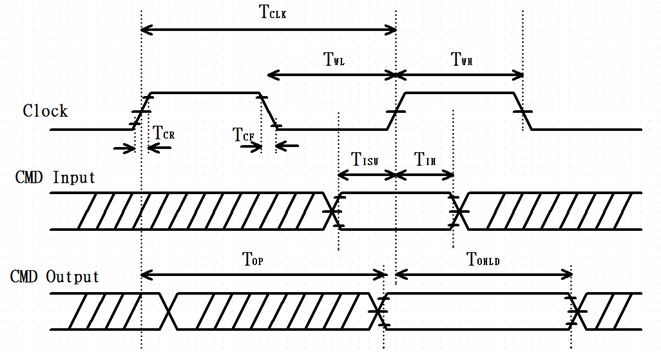
SDIO timing requirements
| Symbol | Parameter | Condition | Min. | Typ. | Max. | Unit |
|---|---|---|---|---|---|---|
| fPP | Clock Frequency | Default Speed High-Speed | 0 0 | - - | 25 50 | MHz |
| TWL | Clock low time | Default Speed High-Speed | 10 7 | - - | - - | ns |
| TWH | Clock high time | Default Speed High-Speed | 10 7 | - - | - - | ns |
| TISU | Input Setup time | Default Speed High-Speed | 5 6 | - - | - - | ns |
| TIH | Input Hold time | Default Speed High-Speed | 5 2 | - - | - - | ns |
| TODLY | Output delay time CL≦40pF (1 card) | Default Speed High-Speed | - - | - - | 14 14 | ns |
| TOH | Output hold time | High-Speed | 2.5 | - | - | ns |
SDR12, SDR25, SDR50 Mode (up to 100 MHz) (VIO_SD 1.8V)
Note: Over full range of values specified in the Recommended Operating Conditions unless otherwise specified.
SDIO timing requirements--- SDR12, SDR25, SDR50 modes (up to 100 MHz) (VIO_SD 1.8V)
| Symbol | Parameter | Condition | Min. | Typ. | Max. | Unit |
|---|---|---|---|---|---|---|
| fPP | Clock Frequency | SDR12/25/50 | 25 | - | 100 | MHz |
| TISU | Input setup time | SDR12/25/50 | 3 | -- | - | ns |
| TIH | Input Hold time | SDR12/25/50 | 0.8 | - | - | ns |
| TCLK | Clock Time | SDR12/25/50 | 10 | - | 40 | ns |
| TCR, TCF | Raise time, Fall time TCR, TCF <2ns (max) at 100 MHz CCARD=10pF | SDR12/25/50 | - | - | 0.2*TCLK | ns |
| TODLY | Output delay time CL≦30pF | SDR12/25/50 | - | - | 7.5 | ns |
| TOH | Output hold time CL=15pF | SDR12/25/50 | 1.5 | - | - | ns |
SDR104 Mode (208 MHz) (VIO_SD 1.8V)
Note: Over full range of values specified in the Recommended Operating Conditions unless otherwise specified.
SDIO timing requirements -- SDR104 modes (up to 208MHz) (VIO_SD 1.8V)
| Symbol | Parameter | Condition | Min. | Typ. | Max. | Unit |
|---|---|---|---|---|---|---|
| fPP | Clock Frequency | SDR104 | 0 | - | 208 | MHz |
| TISU | Input setup time | SDR104 | 1.4 | -- | - | ns |
| TIH | Input hold time | SDR104 | 0.8 | - | - | ns |
| TCLK | Clock time | SDR104 | 4.8 | - | - | ns |
| TCR, TCF | Raise time, Fall time TCR, TCF <0.96ns (max) at 208 MHz CCARD = 10pF | SDR104 | - | - | 0.2*TCLK | ns |
| TOP | Card output phase | SDR104 | 0 | - | 10 | ns |
| TODW | Output timing pf variable data window | SDR12/25/SDR50 | 2.88 | - | - | ns |
DDR50 Mode (50 MHz) (VIO_SD 1.8V)
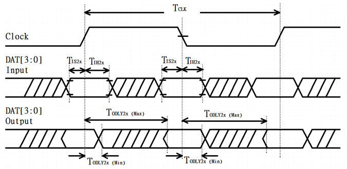
Note: In DDR50 mode, DAT[3:0] lines are samples on both edges of the clock (not applicable for CMD line)
SDIO timing requirements – DDR50 modes (50 MHz)
| Symbol | Parameter | Condition | Min. | Typ. | Max. | Unit | |
|---|---|---|---|---|---|---|---|
| Clock | |||||||
| TCLK | Clock time 50MHz (max) between rising edge | DDR50 | 20 | -- | -- | ns | |
| TCR, TCF | Rise time, fall time TCR, TCF <4.00ns (max) at 50MHz. CCARD=10pF | DDR50 | -- | -- | 0.2*TCLK | ns | |
| Clock Duty | -- | DDR50 | 45 | -- | 55 | % | |
| CMD Input (referenced to clock rising edge) | |||||||
| TIS | Input setup time CCARD≦10pF (1 card) | DDR50 | 6 | -- | -- | ns | |
| TIH | Input hold time CCARD≦10pF (1 card) | DDR50 | 0.8 | -- | -- | ns | |
| CMD Output (referenced to clock rising and failing edge) | |||||||
| TODLY | Output delay time during data transfer mode CL≦30pF (1 card) | DDR50 | -- | -- | 13.7 | ns | |
| TOHLD | Output hold time CL≥15pF (1 card) | DDR50 | 1.5 | -- | -- | ns | |
| DAT[3:0] Input (referenced to clock rising and failing edges) | |||||||
| TIS2X | Input setup time CCARD≦10pF (1 card) | DDR50 | 3 | -- | -- | ns | |
| TIH2X | Input hold time CCARD≦10pF (1 card) | DDR50 | 0.8 | -- | -- | ns | |
| DAT[3:0] Output (referenced to clock rising and failing edges) | |||||||
| TODLY2X (max) | Output delay time during data transfer mode CL≦25pF (1 card) | DDR50 | -- | -- | 7.0 | ns | |
| TODLY2X (min) | Output hold time CL≥15pF (1 card)) | DDR50 | 1.5 | -- | -- | ns | |
SDIO internal pull-up/pull-down specifications
| Parameter | Condition | Min. | Typ. | Max. | Unit |
|---|---|---|---|---|---|
| Internal nominal pull-up/pull-down resistance | -- | 70 | 100 | 140 | kΩ |
High-Speed UART Specification
The NX611 supports a high-speed Universal Asynchronous Receiver/Transmitter (UART)interface, compliant to the industry standard 16550 specification. High-speed baud rates are supported to provide the physical transport between the device and the host for exchanging Bluetooth data. The UART Tx and Rx pins are powered from the VIO voltage supply.
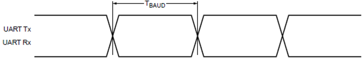
PCM timing specification – master mode
| Symbol | Parameter | Condition | Min. | Typ. | Max. | Unit |
|---|---|---|---|---|---|---|
| TBAUD | Baud rate | 26MHz input clock | 250 | -- | -- | ns |
External Radio Coexistence Interface Specifications
WCI-2 and PTA external coexistence interfaces are used for the coexistence with an external radio. External radios can be connected to the 5-wire packet traffic arbitration interface (PTA) or the 2-wire wireless coexistence interface 2 (WCI-2).
The coexistence architecture has three major components:
- Central hardware Packet Traffic Arbiter (PTA): arbitrates between on-chip Wi-Fi and Bluetooth radios. Controls the front-end components such as RF switches.
- Local hardware arbiter: arbitrates the packets between Bluetooth and Bluetooth Low Energy (LE)
- Coexistence software: configures PTA and works with Wi-Fi and Bluetooth firmware
WCI-2 coexistence interface supports the messages defined in Bluetooth Core Specification Vol 7 Part C for request and grant, where:
The real time message from the external radio to NX611 indicates the request to operate
- MWS_Rx=1 indicates an external radio request to Rx
- MWS_Tx=1 indicates an external radio request to Tx
WCI-2 Coexistence Interface Pins
| Pin name | I/O type | Supply | Description |
|---|---|---|---|
| GPIO25/WCI-2_SIN | I | VIO_GPIO | signal from external radio (input) |
| GPIO26/WCI-2_SOUT | O | VIO_GPIO | External radio state input signal. External radio traffic direction (Tx/Rx) |
PTA Coexistence Interface Pins
| Pin name | I/O type | Supply | Description |
|---|---|---|---|
| GPIO13/EXT_REQ | I | VIO_GPIO | External radio request input signal. |
| GPIO12/EXT_STATE | I | VIO_GPIO | External radio state input signal. External radio traffic direction (Tx/Rx) |
| GPIO14/EXT_GNT | O | VIO_GPIO | Wi-Fi radio wake-up output signal. Multi-functional pin: GPIO[17] input/output |
| GPIO15/EXT_PRI | I | VIO_GPIO | External radio input priority signal |
| GPIO[20]/EXT_FREQ | I | VIO_GPIO | External radio frequency input signal. Frequency overlap between external radio and Wi-Fi. |
Bluetooth Digital Audio Interface Specifications
I2S/PCM Interface Specifications
- Central or peripheral mode
- I2S (Inter-IC Sound) interface for audio data connection to Analog-to-Digital Converters (ADC) and Digital-to- Analog Converters (DAC)
- 3-state I2S interface capability
- I2S pins shared with PCM pins
- Supports clock speeds of 4.096 MHz, 2.048 MHz, and 2 MHz Central or peripheral mode
- PCM bit width size of 8 bits or 16 bits
- Up to 4 slots with configurable bit width and start positions
- 3-state PCM/I2S interface capability
- PCM short frame and long frame5 synchronization
- PCM pins shared with I2S pins
- Supports clock speeds of 4.096 MHz, 2.048 MHz, and 2 MHz
The PCM pins are powered by VIO voltage supply.
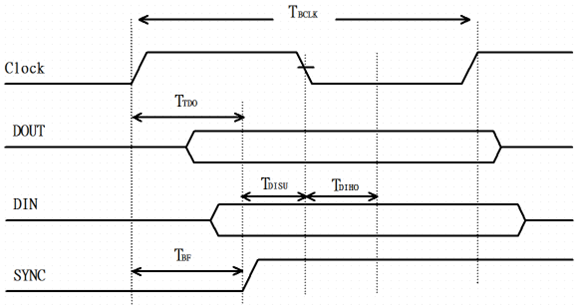
PCM timing specification – master mode
| Symbol | Parameter | Min. | Typ. | Max. | Unit |
|---|---|---|---|---|---|
| FBCLK | - | - | 2/2.048 | - | MHz |
| Duty CycleBCLK | - | 0.4 | 0.5 | 0.6 | - |
| TBCLK rise/fall | - | - | 3 | - | ns |
| TDO | - | - | - | 15 | ns |
| TDISU | - | 20 | - | - | ns |
| TDIHO | - | 15 | - | - | ns |
| TBF | - | - | - | 15 | ns |
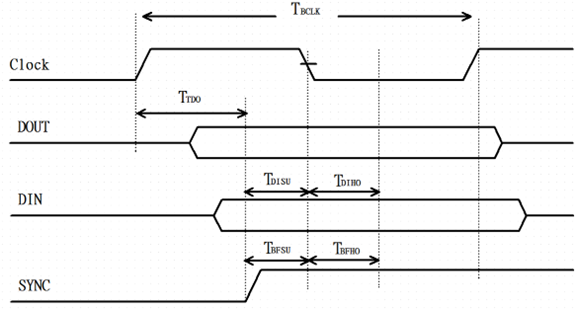
PCM timing specification – slave mode
| Symbol | Parameter | Min. | Typ. | Max. | Unit |
|---|---|---|---|---|---|
| FBCLK | - | - | 2/2.048 | - | MHz |
| Duty CycleBCLK | - | 0.4 | 0.5 | 0.6 | - |
| TBCLK rise/fall | - | - | 3 | - | ns |
| TDO | - | - | - | 30 | ns |
| TDISU | - | 15 | - | - | ns |
| TDIHO | - | 10 | - | - | ns |
| TBFSU | - | 15 | - | - | Ns |
| TBFHO | - | 10 | - | - | Ns |
Electrical Characteristics
Absolute Maximum Ratings
Absolute maximum ratings are those values beyond which damage to the device can occur. Functional operation under these conditions, or at any other condition beyond those indicated in the operational sections of this document, is not recommended.
Note: Maximum rating for signals follows the supply domain of the signals.
| Symbol (Domain) | Parameter | Max Rating | Unit |
|---|---|---|---|
| VIO_SD | WLAN host SDIO interface I/O supply (for 1.8V system) (for 3.3V system) | 2.16 3.96 | V |
| VIO | I/O configuration power supply (for 1.8V system) (for 3.3V system) | 2.16 3.96 | V |
| AVDD33 | External DC power supply | 3.96 | V |
| Storage | Storage temperature | -55 +125 | °C |
| ESD | Electrostatic discharge tolerance | 2000 | V |
Recommended Operating Conditions
| Symbol (Domain) | Parameter | Min | Typ | Max | Unit |
|---|---|---|---|---|---|
| VIO_SD | WLAN and Bluetooth host interface I/O supply | 1.71/3.14 | 1.8/3.3 | 1.89/3.46 | V |
| VIO | I/O supply for the RF switch control pads | 1.71/3.14 | 1.8/3.3 | 1.89/3.46 | V |
| AVDD33 | External DC power supply | 3.14 | 3.3 | 3.46 | V |
| T-ambient | Ambient temperature | -40 | 25 | 85 | °C |
DC Electrical Characteristics
The following tables list the general DC electrical characteristics over recommended operating conditions (unless otherwise specified).
General DC electrical characteristics (For 1.8V or 3.3V operation VIO)
| Symbol | Parameter | Conditions | Min | Typ | Max | Unit |
|---|---|---|---|---|---|---|
| VIH | High Level Input Voltage | — | 0.7*VIO | — | VIO+0.4 | V |
| VIL | Low Level Input Voltage | — | -0.4 | — | 0.3*VIO | V |
| VOH | Output high Voltage | — | VIO-0.4 | — | — | V |
| VOL | Output low Voltage | — | — | — | 0.4 | V |
General DC electrical characteristics (For 1.8V or 3.3V operation VIO_SD)
| Symbol | Parameter | Conditions | Min | Typ | Max | Unit |
|---|---|---|---|---|---|---|
| VIH | High Level Input Voltage | — | 0.7*VIO_SD | — | VIO_SD+0.4 | V |
| VIL | Low Level Input Voltage | — | -0.4 | — | 0.3*VIO_SD | V |
| VOH | Output high Voltage | — | VIO_SD-0.4 | — | — | V |
| VOL | Output low Voltage | — | — | — | 0.4 | V |
Current Consumption
NX611 SIP Module Current Consumption
Note: Unless otherwise stated, all specifications are at 25°C, nominal voltage, and typical value with SDIO 2.0, measured on Dev Kit, Sona NX611 SIP, 1 RF Trace Pin Part Number 453-00156-K1.
25 MHz clock (4-bit mode)
| Mode | Conditions | 1.8V | 3.3V[11] [7] | Unit |
|---|---|---|---|---|
| Power down | ||||
| Power Down | - | 0.019 | 0.007 | mA |
| Sleep Mode | ||||
| Bluetooth only in deep sleep mode | - | 0.25 | 0.14 | mA |
| Wi-Fi only in deep sleep mode | SDIO 3.0 200 MHz VIO = 1.8 V | 0.36 | 0.02 | mA |
| Wi-Fi and Bluetooth in deep sleep Mode | - | 0.41 | 0.14 | mA |
| Bluetooth LE current consumption | ||||
| Bluetooth LE peak transmit [3] | 1 Mbps @ 6 dBm | 177 | .179 | mA |
| Bluetooth LE peak receive[4][5] | 1 Mbps | 0.11 | 0.33 | mA |
| Bluetooth current consumption [2] | ||||
| Bluetooth peak transmit[6] | @ 6 dBm DH5 | 167 | .116 | mA |
| Bluetooth peak receive[4][7] | BDR , DH5 | 39 | 0.33 | mA |
| 2.4 GHz Wi-Fi receive[8] | ||||
| 2.4 GHz 802.11b 11 Mbps | — | 94 | 0.065 | mA |
| 2.4 GHz 802.11g 54 Mbps | — | 102 | 0.065 | mA |
| 2.4 GHz 802.11n 20 MHz MCS7 | — | 102 | 0.065 | mA |
| 2.4 GHz 802.11n 40 MHz MCS7 | — | 117 | 0.065 | mA |
| 2.4 GHz 802.11ax 20 MHz MCS11 | — | 105 | 0.065 | mA |
| 2.4 GHz 802.11ax 40 MHz MCS11 | — | 119 | 0.065 | mA |
| 5 GHz Wi-Fi receive[8] | 0.065 | |||
| 5 GHz 802.11a 54 Mbps | — | 117 | 0.065 | mA |
| 5 GHz 802.11n 20 MHz MCS7 | — | 117 | 0.065 | mA |
| 5 GHz 802.11n 40 MHz MCS7 | — | 126 | 0.065 | mA |
| 5 GHz 802.11ac 40 MHz MCS9 | — | 146 | 0.065 | mA |
| 5 GHz 802.11ac 80 MHz MCS9 | — | 167 | 0.065 | mA |
| 5 GHz 802.11ax 20 MHz MCS11 | — | 117 | 0.065 | mA |
| 5 GHz 802.11ax 40 MHz MCS11 | — | 146 | 0.065 | mA |
| 5 GHz 802.11ax 80 MHz MCS11 | — | 1 | 0.065 | mA |
| 2.4 GHz Wi-Fi transmit[8] | ||||
| 2.4 GHz 802.11b 11 Mbps @ 18 dBm | — | 149 | 220 | mA |
| 2.4 GHz 802.11g 54 Mbps @ 16 dBm | — | 160 | 178 | mA |
| 2.4 GHz 802.11n 20 MHz MCS7 @ 15 dBm | — | 159 | 163 | mA |
| 2.4 GHz 802.11n 40 MHz MCS7 @ 15 dBm | — | 163 | 156 | mA |
| 2.4 GHz 802.11ax 20 MHz MCS11 @ 13 dBm | — | 163 | 149 | mA |
| 2.4 GHz 802.11ax 40 MHz MCS11 @ 13 dBm | — | 163 | 174 | mA |
| 5 GHz Wi-Fi transmit[8] | ||||
| 5 GHz 802.11a 6 Mbps @ 16 dBm | — | 226 | 261 | mA |
| 5 GHz 802.11a 54 Mbps @ 16 dBm | — | 218 | 244 | mA |
| 5 GHz 802.11n 20 MHz MCS7 @ 14 dBm | — | 213 | 201 | mA |
| 5 GHz 802.11n 40 MHz MCS7 @ 14 dBm | — | 214 | 202 | mA |
| 5 GHz 802.11ac 20 MHz MCS8 @ 14 dBm | — | 213 | 201 | mA |
| 5 GHz 802.11ac 40 MHz MCS9 @ 12 dBm | — | 203 | 163 | mA |
| 5 GHz 802.11ac 80 MHz MCS9 @ 12 dBm | — | 216 | 156 | mA |
| 5 GHz 802.11ax 20 MHz MCS11 @ 10 dBm | — | 197 | 140 | mA |
| 5 GHz 802.11ax 40 MHz MCS11 @ 10 dBm | — | 202 | 142 | mA |
| 5 GHz 802.11ax 80 MH MCS11 @ 10 dBm | — | 218 | 144 | mA |
| Peak current | ||||
| Peak current during device initialization | — | 371 | 139 | mA |
[1] SDIO host interface connected
[2] Wi-Fi enabled, SDIO host interface connected
[3] The peak transmit current remains the same across all Bluetooth LE data rates at the same transmit power level
[4] Single antenna configuration
[5] The peak receive current remains the same across all Bluetooth LE data rates
[6] The peak transmit current remains the same across all Bluetooth data rates at the same transmit power level
[7] The peak receive current remains the same across all Bluetooth data rates
[8] Bluetooth enabled
[9] Frame length in IEEE-PS current measurement: 5 GHz: 207 Bytes, 2.4 GHz: 222 Bytes
[10] Maximum value
[11] VIO, VIO_SD 3.3V
NX611 M.2 1216/ M.2 2230 Current Consumption
Note: Unless otherwise stated, all specifications are at 25°C, nominal voltage, and typical value with SDIO 3.0, measured on Dev Kit, Sona NX611 M.2 2230, 1 MHF4 Part Number 453-00166-K1.
25 MHz clock (4-bit mode)
| Mode | Conditions | 1.8V_VIO | 3.3V | Unit |
|---|---|---|---|---|
| Power down | ||||
| Power Down | - | 1.7 | .348 | mA |
| Sleep Mode | ||||
| Bluetooth only in deep sleep mode | - | 0.37 | 0.02 | mA |
| Wi-Fi only in deep sleep mode | SDIO 3.0 200 MHz VIO = 1.8 V | 1.8 | 0.02 | mA |
| Wi-Fi and Bluetooth in deep sleep Mode | - | 0.53 | 0.02 | mA |
| Bluetooth LE current consumption | ||||
| Bluetooth LE peak transmit [3] | 1 Mbps @ 6 dBm | 0.014 | 106 | mA |
| Bluetooth LE peak receive[4][5] | 1 Mbps | .009 | 75 | mA |
| Bluetooth current consumption [2] | ||||
| Bluetooth peak transmit[6] | @ 6 dBm DH5 | .009 | 113 | mA |
| Bluetooth peak receive[4][7] | BDR , DH5 | .009 | 75 | mA |
| 2.4 GHz Wi-Fi receive[8] | ||||
| 2.4 GHz 802.11b 11 Mbps | — | .009 | 56 | mA |
| 2.4 GHz 802.11g 54 Mbps | — | .009 | 59 | mA |
| 2.4 GHz 802.11n 20 MHz MCS7 | — | .009 | 61 | mA |
| 2.4 GHz 802.11n 40 MHz MCS7 | — | .009 | 62 | mA |
| 2.4 GHz 802.11ax 20 MHz MCS11 | — | .009 | 63 | mA |
| 2.4 GHz 802.11ax 40 MHz MCS11 | — | .009 | 66 | mA |
| 5 GHz Wi-Fi receive[8] | ||||
| 5 GHz 802.11a 54 Mbps | — | .009 | 62 | mA |
| 5 GHz 802.11n 20 MHz MCS7 | — | .009 | 68 | mA |
| 5 GHz 802.11n 40 MHz MCS7 | — | .009 | 65 | mA |
| 5 GHz 802.11ac 40 MHz MCS9 | — | .009 | 83 | mA |
| 5 GHz 802.11ac 80 MHz MCS9 | — | .009 | 92 | mA |
| 5 GHz 802.11ax 20 MHz MCS11 | — | .009 | 70 | mA |
| 5 GHz 802.11ax 40 MHz MCS11 | — | .009 | 79 | mA |
| 5 GHz 802.11ax 80 MHz MCS11 | — | .009 | 96 | mA |
| 2.4 GHz Wi-Fi transmit[8] | ||||
| 2.4 GHz 802.11b 11 Mbps @ 18 dBm | — | .009 | 296 | mA |
| 2.4 GHz 802.11g 54 Mbps @ 16 dBm | — | .009 | 258 | mA |
| 2.4 GHz 802.11n 20 MHz MCS7 @ 15 dBm | — | .009 | 252 | mA |
| 2.4 GHz 802.11n 40 MHz MCS7 @ 15 dBm | — | .009 | 248 | mA |
| 2.4 GHz 802.11ax 20 MHz MCS11 @ 13 dBm | — | .009 | 231 | mA |
| 2.4 GHz 802.11ax 40 MHz MCS11 @ 13 dBm | — | .009 | 229 | mA |
| 5 GHz Wi-Fi transmit[8] | ||||
| 5 GHz 802.11a 6 Mbps @ 16 dBm | — | .009 | 331 | mA |
| 5 GHz 802.11a 54 Mbps @ 16 dBm | — | .009 | 314 | mA |
| 5 GHz 802.11n 20 MHz MCS7 @ 14 dBm | — | .009 | 292 | mA |
| 5 GHz 802.11n 40 MHz MCS7 @ 14 dBm | — | .009 | 293 | mA |
| 5 GHz 802.11ac 20 MHz MCS8 @ 14 dBm | — | .009 | 292 | mA |
| 5 GHz 802.11ac 40 MHz MCS9 @ 12 dBm | — | .009 | 273 | mA |
| 5 GHz 802.11ac 80 MHz MCS9 @ 12 dBm | — | .009 | 268 | mA |
| 5 GHz 802.11ax 20 MHz MCS11 @ 10 dBm | — | .009 | 254 | mA |
| 5 GHz 802.11ax 40 MHz MCS11 @ 10 dBm | — | .009 | 248 | mA |
| 5 GHz 802.11ax 80 MH MCS11 @ 10 dBm | — | .009 | 262 | mA |
| Peak current | ||||
| Peak current during device initialization | 571 | .140 | mA |
[1] SDIO host interface connected
[2] Wi-Fi enabled, SDIO host interface connected
[3] The peak transmit current remains the same across all Bluetooth LE data rates at the same transmit power level
[4] Single antenna configuration
[5] The peak receive current remains the same across all Bluetooth LE data rates
[6] The peak transmit current remains the same across all Bluetooth data rates at the same transmit power level
[7] The peak receive current remains the same across all Bluetooth data rates
[8] Bluetooth enabled
[9] Frame length in IEEE-PS current measurement: 5 GHz: 207 Bytes, 2.4 GHz: 222 Bytes
[10] Maximum value
Radio Characteristics
WLAN Radio Receiver Characteristics
Typical WLAN receiver characteristics for 2.4 GHz Band, WLAN Channels 1-11, single chain operation at 25 degrees C, ambient temperature.
| 2.4 GHz Wi-Fi Receive Sensitivity | Conditions | 1-Port | 2-Port | Unit |
|---|---|---|---|---|
| 2.4 GHz 802.11b 1 Mbps | 8% PER | -96.5 | -97.5 | dBm |
| 2.4 GHz 802.11b 11 Mbps | 8% PER | -88.0 | -89.0 | dBm |
| 2.4 GHz 802.11g 6 Mbps | 10% PER | -91.0 | -92.0 | dBm |
| 2.4 GHz 802.11g 54 Mbps | 10% PER | -74.5 | -75.5 | dBm |
| 2.4 GHz 802.11n 20 MHz MCS0 | 10% PER | -90.5 | -91.5 | dBm |
| 2.4 GHz 802.11n 20 MHz MCS7 | 10% PER | -71 | -72 | dBm |
| 2.4 GHz 802.11n 40 MHz MCS0 | 10% PER | -87.5 | -88.5 | dBm |
| 2.4 GHz 802.11n 40 MHz MCS7 | 10% PER | -68.5 | -69.5 | dBm |
| 2.4 GHz 802.11ax 20 MHz MCS0 | 10% PER | -91 | -92 | dBm |
| 2.4 GHz 802.11ax 20 MHz MCS11 | 10% PER | -61.5 | -62.5 | dBm |
| 2.4 GHz 802.11ax 40 MHz MCS0 | 10% PER | -87.5 | -88.5 | dBm |
| 2.4 GHz 802.11ax 40 MHz MCS11 | 10% PER | -59.5 | -60.5 | dBm |
| 2.4 GHz Receiver maximum input level (MIL) | Conditions | 1-port | 2-port | Unit |
| Receiver maximum input level DSSS | 802.11b DSSS MIL | 0 | 0 | dBm |
| Receiver maximum input level CCK | 802.11b CCK MIL | 0 | 0 | dBm |
| Receiver maximum input level OFDM | OFDM MIL | -10 | -10 | dBm |
| Receiver adjacent channel interference (ACI) | Conditions | 1-port | 2-port | Unit |
| Receiver ACI 802.11b | 20 MHz 1 Mbps | 53 | 53 | dB |
| Receiver ACI 802.11b | 20 MHz 11 Mbps | 47.7 | 47.7 | dB |
| Receiver ACI 802.11g | 20 MHz 6 Mbps | 30.3 | 30.3 | dB |
| Receiver ACI 802.11g | 20 MHz 54 Mbps | 27.3 | 27.3 | dB |
| Receiver ACI 802.11n | 20 MHz MCS0 Nss1 BCC | 41 | 41 | dB |
| Receiver ACI 802.11n | 20 MHz MCS7 Nss1 BCC | 27.3 | 27.3 | dB |
| Receiver ACI 802.11ax | 20 MHz MCS0 Nss1 LDPC[1] | 30.3 | 30.3 | dB |
| Receiver ACI 802.11ax | 20 MHz MCS11 Nss1 LDPC[1] | 7 | 7 | dB |
| Receiver Alternate Adjacent channel interference (AACI) | Conditions | 1-port | 2-port | Unit |
| Receiver AACI 802.11b | 20 MHz 1 Mbps | 53 | 53 | dB |
| Receiver AACI 802.11b | 20 MHz 11 Mbps | 49 | 49 | dB |
| Receiver AACI 802.11g | 20 MHz 6 Mbps | 49 | 49 | dB |
| Receiver AACI 802.11g | 20 MHz 54 Mbps | 33.3 | 33.3 | dB |
| Receiver AACI 802.11n | 20 MHz MCS0 Nss1 BCC | 49.7 | 49.7 | dB |
| Receiver AACI 802.11n | 20 MHz MCS7 Nss1 BCC | 32.3 | 32.3 | dB |
| Receiver AACI 802.11ax | 20 MHz MCS0 Nss1 LDPC[1] | 48.7 | 48.7 | dB |
| Receiver AACI 802.11ax | 20 MHz MCS11 Nss1 LDPC[1] | 23.3 | 23.3 | dB |
Typical WLAN receiver characteristics for 5 GHz Channels 36-48, 52-64,100-140,149-165, Band, Channels single chain operation at 25 degrees C ambient temperature.
| 5 GHz Wi-Fi Receive Sensitivity | Conditions% PER | 1- and 2-port | Unit |
|---|---|---|---|
| 5 GHz 802.11a 6 Mbps | 10% PER | -89.5 | dBm |
| 5 GHz 802.11a 54 Mbps | 10% PER | -72.5 | dBm |
| 5 GHz 802.11n 20 MHz MCS0 | 10% PER | -88.5 | dBm |
| 5 GHz 802.11n 20 MHz MCS7 | 10% PER | -69.0 | dBm |
| 5 GHz 802.11n 40 MHz MCS0 | 10% PER | -85.5 | dBm |
| 5 GHz 802.11n 40 MHz MCS7 | 10% PER | -66.5 | dBm |
| 5 GHz 802.11ac 20 MHz MCS0 | 10% PER | -89.5 | dBm |
| 5 GHz 802.11ac 20 MHz MCS8 | 10% PER | -66.5 | dBm |
| 5 GHz 802.11ac 40 MHz MCS0 | 10% PER | -86.0 | dBm |
| 5 GHz 802.11ac 40 MHz MCS9 | 10% PER | -63.5 | dBm |
| 5 GHz 802.11ac 80 MHz MCS0 | 10% PER | -82.5 | dBm |
| 5 GHz 802.11ac 80 MHz MCS9 | 10% PER | -60.5 | dBm |
| 5 GHz 802.11ax 20 MHz MCS0 | 10% PER | -89.5 | dBm |
| 5 GHz 802.11ax 20 MHz MCS11 | 10% PER | -68.0 | dBm |
| 5 GHz 802.11ax 40 MHz MCS0 | 10% PER | -82.5 | dBm |
| 5 GHz 802.11ax 40 MHz MCS11 | 10% PER | -57.5 | dBm |
| 5 GHz 802.11ax 80 MHz MCS0 | 10% PER | -82.5 | dBm |
| 5 GHz 802.11ax 80 MHz MCS11 | 10% PER | -60.5 | dBm |
| 5 GHz Receiver Maximum Input Level (MIL) | Conditions | 1- and 2-port | Unit |
| 5 GHz Receiver maximum input level OFDM | OFDM MIL | -10 | dBm |
| Receiver adjacent channel interference (ACI) | Conditions | 1- and 2-port | Unit |
| Receiver ACI 802.11a | 20 MHz 6 Mbps | 23 | dBm |
| Receiver ACI 802.11a | 20 MHz 54 Mbps | 15.7 | dBm |
| Receiver ACI 802.11n | 20 MHz MCS0 Nss1 BCC | 28 | dBm |
| Receiver ACI 802.11n | 20 MHz MCS7 Nss1 BCC | 10 | dBm |
| Receiver ACI 802.11n | 40 MHz MCS0 Nss1 BCC | 27.3 | dBm |
| Receiver ACI 802.11n | 40 MHz MCS7 Nss1 BCC | 13 | dBm |
| Receiver ACI 802.11ac | 20 MHz MCS0 Nss1 LDPC | 31.3 | dBm |
| Receiver ACI 802.11ac | 20 MHz MCS9 Nss1 LDPC | 15 | dBm |
| Receiver ACI 802.11ac | 40 MHz MCS0 Nss1 LDPC | 29.7 | dBm |
| Receiver ACI 802.11ac | 40 MHz MCS9 Nss1 LDPC | 12.3 | dBm |
| Receiver ACI 802.11ac | 80 MHz MCS0 Nss1 LDPC | 25 | dBm |
| Receiver ACI 802.11ac | 80 MHz MCS9 Nss1 LDPC | 13 | dBm |
| Receiver AACI 802.11a | 20 MHz 6 Mbps | 47.3 | dB |
| Receiver AACI 802.11a | 20 MHz 54 Mbps | 27.7 | dB |
| Receiver AACI 802.11n | 20 MHz MCS0 Nss1 BCC | 46.3 | dB |
| Receiver AACI 802.11n | 20 MHz MCS7 Nss1 BCC | 30 | dB |
| Receiver AACI 802.11n | 40 MHz MCS0 Nss1 BCC | 45 | dB |
| Receiver AACI 802.11a | 20 MHz 6 Mbps | 47.3 | dB |
| Receiver AACI 802.11a | 20 MHz 54 Mbps | 27.7 | dB |
| Receiver AACI 802.11n | 20 MHz MCS0 Nss1 BCC | 46.3 | dB |
| Receiver AACI 802.11n | 20 MHz MCS7 Nss1 BCC | 30 | dB |
| Receiver AACI 802.11n | 40 MHz MCS0 Nss1 BCC | 45 | dB |
| Receiver AACI 802.11n | 40 MHz MCS7 Nss1 BCC | 27 | dB |
| Receiver AACI 802.11ac | 20 MHz MCS0 Nss1 LDPC | 45.7 | dB |
| Receiver AACI 802.11ac | 20 MHz MCS9 Nss1 LDPC | 29.3 | dB |
| Receiver AACI 802.11ac | 40 MHz MCS0 Nss1 LDPC | 44.7 | dB |
| Receiver AACI 802.11ac | 40 MHz MCS9 Nss1 LDPC | 23 | dB |
| Receiver AACI 802.11ac | 80 MHz MCS0 Nss1 LDPC | 43.3 | dB |
| Receiver AACI 802.11ac | 80 MHz MCS9 Nss1 LDPC | 24 | dB |
| Receiver AACI 802.11ax | 20 MHz MCS0 Nss1 LDPC[1] | 48 | dB |
| Receiver AACI 802.11ax | 20 MHz MCS11 Nss1 LDPC[1] | 21.3 | dB |
| Receiver AACI 802.11ax | 40 MHz MCS0 Nss1 LDPC[1] | 45 | dB |
| Receiver AACI 802.11ax | 40 MHz MCS11 Nss1 LDPC[1] | 19.7 | dB |
| Receiver AACI 802.11ax | 80 MHz MCS0 Nss1 LDPC[1] | 44 | dB |
| Receiver AACI 802.11ax | 80 MHz MCS11 Nss1 LDPC[1] | 18.3 | dB |
WLAN Transmitter Characteristics
Typical WLAN transmitter characteristics for 2.4 GHz band operation (VDD=3.3V, VIO=1.8V), WLAN Channels 1-11, single chain operation at 25 degrees C, ambient temperature.
| 2.4 GHz Wi-Fi Transmit Power | Conditions | 1-Port | 2-Port | Unit |
|---|---|---|---|---|
| 2.4 GHz 802.11b 1 Mbps | -9.1 dB, EVM, Mask Compliance | 18 | 18 | dBm |
| 2.4 GHz 802.11b 11 Mbps | -9.1 dB, EVM, Mask Compliance | 18 | 18 | dBm |
| 2.4 GHz 802.11g 6 Mbps | -5 dB, EVM, Mask Compliance | 14 | 14 | dBm |
| 2.4 GHz 802.11g 54 Mbps | -25 dB, EVM, Mask Compliance | 14 | 14 | dBm |
| 2.4 GHz 802.11n 20 MHz MCS0 | -5 dB, EVM, Mask Compliance | 14 | 14 | dBm |
| 2.4 GHz 802.11n 20 MHz MCS7 | -27 dB, EVM, Mask Compliance | 14 | 14 | dBm |
| 2.4 GHz 802.11n 40 MHz MCS0 | -5 dB, EVM, Mask Compliance | 12 | 12 | dBm |
| 2.4 GHz 802.11n 40 MHz MCS7 | -27 dB, EVM, Mask Compliance | 12 | 12 | dBm |
| 2.4 GHz 802.11ax 20 MHz MCS0 | -5 dB, EVM, Mask Compliance | 13 | 13 | dBm |
| 2.4 GHz 802.11ax 20 MHz MCS11 | -35 dB, EVM, Mask Compliance | 13 | 13 | dBm |
| 2.4 GHz 802.11ax 40 MHz MCS0 | -5 dB, EVM, Mask Compliance | 13 | 13 | dBm |
| 2.4 GHz 802.11ax 40 MHz MCS11 | -35 dB, EVM, Mask Compliance | 11 | 11 | dBm |
Typical WLAN Transmitter characteristics for 5 GHz band operation, (VDD=3.3V, VIO=1.8V), Channels 36-48, 52-64,100-140,149-165, Band, Channels single chain operation at 25 degrees C ambient.
| 5 GHz Wi-Fi Transmit Power | Conditions% PER | 1- and 2-port | Unit |
|---|---|---|---|
| 5 GHz 802.11a 6 Mbps | -5 dB, EVM, Mask Compliance | 16 | dBm |
| 5 GHz 802.11a 54 Mbps | -25 dB, EVM, Mask Compliance | 16 | dBm |
| 5 GHz 802.11n 20 MHz MCS0 | -5 dB, EVM, Mask Compliance | 14 | dBm |
| 5 GHz 802.11n 20 MHz MCS7 | -5 dB, EVM, Mask Compliance | 14 | dBm |
| 5 GHz 802.11n 40 MHz MCS0 | -5 dB, EVM, Mask Compliance | 13 | dBm |
| 5 GHz 802.11n 40 MHz MCS7 | -27 dB, EVM, Mask Compliance | 13 | dBm |
| 5 GHz 802.11ac 20 MHz MCS0 | -5 dB, EVM, Mask Compliance | 14 | dBm |
| 5 GHz 802.11ac 20 MHz MCS8 | -30 dB, EVM, Mask Compliance | 14 | dBm |
| 5 GHz 802.11ac 40 MHz MCS0 | -5 dB, EVM, Mask Compliance | 13 | dBm |
| 5 GHz 802.11ac 40 MHz MCS9 | -32 dB, EVM, Mask Compliance | 13 | dBm |
| 5 GHz 802.11ac 80 MHz MCS0 | -5 dB, EVM, Mask Compliance | 11 | dBm |
| 5 GHz 802.11ac 80 MHz MCS9 | -32 dB, EVM, Mask Compliance | 11 | dBm |
| 5 GHz 802.11ax 20 MHz MCS0 | -5 dB, EVM, Mask Compliance | 13 | dBm |
| 5 GHz 802.11ax 20 MHz MCS11 | -35 dB, EVM, Mask Compliance | 10 | dBm |
| 5 GHz 802.11ax 40 MHz MCS0 | -5 dB, EVM, Mask Compliance | 13 | dBm |
| 5 GHz 802.11ax 40 MHz MCS11 | -35 dB, EVM, Mask Compliance | 10 | dBm |
| 5 GHz 802.11ax 80 MHz MCS0 | -5 dB, EVM, Mask Compliance | 10 | dBm |
| 5 GHz 802.11ax 80 MHz MCS11 | -35 dB, EVM, Mask Compliance | 10 | dBm |
Bluetooth Transmitter Characteristics
Bluetooth Radio Receiver Characteristics
Typical Bluetooth/Bluetooth LE receiver performance at AVDD33=3.3 VDC and VIO=1.8 V, 25 degrees C, ambient temperature.
| Parameter | Conditions | Min | Typ | Max | Unit |
| Frequency range | -- | 2400 | -- | 2483.5 | MHz |
| Receiver sensitivity | Conditions | 1-Port | 2-Port | Unit | |
| BDR 1 Mbps | 0.1% BER, 1DH5 | -92 | -93 | dBm | |
| EDR 2 Mbps | 0.01% BER,2DH5 | -91 | -92 | dBm | |
| EDR 3 Mbps | 0.01% BER,3DH5 | -86 | -87 | dBm | |
| Bluetooth LE 1 Mbps | 0.1% BER, 37 Packet Payload, TX Impairments [1] | -95.5 | -96.5 | dBm | |
| Bluetooth LE 2 Mbps | 0.1% BER, 37 Packet Payload, TX Impairments [1] | -93 | -94 | dBm | |
| Bluetooth LR 500 Kbps | 0.1% BER, 37 Packet Payload, TX Impairments [1] | -97 | -98 | dBm | |
| Bluetooth LR 125 Kbps | 0.1% BER, 37 Packet Payload, TX Impairments [1] | -102 | -103 | dBm | |
| Receiver maximum input level (MIL) | Conditions | 1-Port | 2-Port | Unit | |
| BDR 1 Mbps | [2] | -2 | -3 | dBm | |
| EDR 2 Mbps | [3] | -5 | -6 | dBm | |
| EDR 3 Mbps | [4] | -5 | -6 | dBm | |
| Bluetooth LE 1 Mbps | [5] | -2 | -3 | dBm | |
| Bluetooth LE 2 Mbps | [6] | -2 | -3 | dBm | |
| Bluetooth LR 500 Kbps | [7] | -2 | -3 | dBm | |
| Bluetooth LR 125 Kbps | [8] | -2 | -3 | dBm | |
| Receiver Adjacent-/Co- Channel Interference (ACI/CCI) | |||||
| BDR 1 Mbps | |||||
| Receiver ACI @ -5 MHz (image -1) | BDR 1 Mbps | -38 | -38 | dB | |
| Receiver ACI @ -4 MHz (image) | BDR 1 Mbps | -26 | -26 | dB | |
| Receiver ACI @ -3 MHz (image +1) | BDR 1 Mbps | -41 | -41 | dB | |
| Receiver ACI @ -2 MHz | BDR 1 Mbps | -46 | -46 | dB | |
| Receiver ACI @ -1 MHz | BDR 1 Mbps | -9 | -9 | dB | |
| Receiver CCI | BDR 1 Mbps | 11 | 11 | dB | |
| Receiver ACI @ +1 MHz | BDR 1 Mbps | -11 | -11 | dB | |
| Receiver ACI @ +2 MHz | BDR 1 Mbps | -49 | -49 | dB | |
| Receiver ACI @ +3 MHz | BDR 1 Mbps | -52 | -52 | dB | |
| BDR 2 Mbps | |||||
| Receiver ACI @ -5 MHz (image -1) | BDR 2 Mbps | -42 | -42 | dB | |
| Receiver ACI @ -4 MHz (image) | BDR 2 Mbps | -28 | -28 | dB | |
| Receiver ACI @ -3 MHz (image +1) | BDR 2 Mbps | -41 | -41 | dB | |
| Receiver ACI @ -2 MHz | BDR 2 Mbps | -46 | -46 | dB | |
| Receiver ACI @ -1 MHz | BDR 2 Mbps | -9 | -9 | dB | |
| Receiver CCI | BDR 2 Mbps | 10 | 10 | dB | |
| Receiver ACI @ +1 MHz | BDR 2 Mbps | -11 | -11 | dB | |
| Receiver ACI @ +2 MHz | BDR 2 Mbps | -49 | -49 | dB | |
| Receiver ACI @ +3 MHz | BDR 2 Mbps | -52 | -52 | dB | |
| BDR 3 Mbps | |||||
| Receiver ACI @ -5 MHz (image -1) | BDR 3 Mbps | -38 | -38 | dB | |
| Receiver ACI @ -4 MHz (image) | BDR 3 Mbps | -20 | -20 | dB | |
| Receiver ACI @ -3 MHz (image +1) | BDR 3 Mbps | -38 | -38 | dB | |
| Receiver ACI @ -2 MHz | BDR 3 Mbps | -41 | -41 | dB | |
| Receiver ACI @ -1 MHz | BDR 3 Mbps | -8 | -8 | dB | |
| Receiver CCI | BDR 3 Mbps | 16 | 16 | dB | |
| Receiver ACI @ +1 MHz | BDR 3 Mbps | -8 | -8 | dB | |
| Receiver ACI @ +2 MHz | BDR 3 Mbps | -42 | -42 | dB | |
| Receiver ACI @ +3 MHz | BDR 3 Mbps | -48 | -48 | dB | |
| Bluetooth LE 1 Mbps | |||||
| Receiver ACI @ -5 MHz (image -1) | BLE 1 Mbps | -39 | -39 | dB | |
| Receiver ACI @ -4 MHz (image) | BLE 1 Mbps | -28 | -28 | dB | |
| Receiver ACI @ -3 MHz (image +1) | BLE 1 Mbps | -38 | -38 | dB | |
| Receiver ACI @ -2 MHz | BLE 1 Mbps | -45 | -45 | dB | |
| Receiver ACI @ -1 MHz | BLE 1 Mbps | -3 | -3 | dB | |
| Receiver CCI | BLE 1 Mbps | 9 | 9 | dB | |
| Receiver ACI @ +1 Mbps | BLE 1 Mbps | -9 | -9 | dB | |
| Receiver ACI @ +2 Mbps | BLE 1 Mbps | -50 | -50 | dB | |
| Receiver ACI @ +3 Mbps | BLE 1 Mbps | -52 | -52 | dB | |
| Bluetooth LE 2 Mbps | |||||
| Receiver ACI @ -6 MHz (image -2) | BLE 2 Mbps | -51 | -51 | dB | |
| Receiver ACI @ -4 MHz (image) | BLE 2 Mbps | -29 | -29 | dB | |
| Receiver ACI @ -2 MHz | BLE 2 Mbps | -19 | -19 | dB | |
| Receiver CCI | BLE 2 Mbps | 8 | 8 | dB | |
| Receiver ACI @+2 Mbps | BLE 2 Mbps | -29 | -29 | dB | |
| Receiver ACI @ +4 Mbps | BLE 2 Mbps | -51 | -51 | dB | |
| Receiver ACI @ +6 Mbps | BLE 2 Mbps | -55 | -55 | dB | |
| Bluetooth LR 500 kbps | |||||
| Receiver ACI @ -5 MHz (image -1) | Bluetooth LR 500 kbps | -40 | -40 | dB | |
| Receiver ACI @ -4 MHz (image) | Bluetooth LR 500 kbps | -28 | -28 | dB | |
| Receiver ACI @ -3 MHz (image +1) | Bluetooth LR 500 kbps | -38 | -38 | dB | |
| Receiver ACI @ -2 MHz | Bluetooth LR 500 kbps | -48 | -48 | dB | |
| Receiver ACI @ -1 MHz | Bluetooth LR 500 kbps | -5 | -5 | dB | |
| Receiver CCI | Bluetooth LR 500 kbps | 9 | 9 | dB | |
| Receiver ACI @ 1 Mbps | Bluetooth LR 500 kbps | -11 | -11 | dB | |
| Receiver ACI @ 2 Mbps | Bluetooth LR 500 kbps | -51 | -51 | dB | |
| Receiver ACI @ 3 Mbps | Bluetooth LR 500 kbps | -55 | -55 | dB | |
| Bluetooth LR 125 kbps | |||||
| Receiver ACI @ -5 MHz (image -1) | Bluetooth LR 125 kbps | -41 | -41 | dB | |
| Receiver ACI @ -4 MHz (image) | Bluetooth LR 125 kbps | -28 | -28 | dB | |
| Receiver ACI @ -3 MHz (image +1) | Bluetooth LR 125 kbps | -39 | -39 | dB | |
| Receiver ACI @ -2 MHz | Bluetooth LR 125 kbps | -49 | -49 | dB | |
| Receiver ACI @ -1 MHz | Bluetooth LR 125 kbps | -5 | -5 | dB | |
| Receiver CCI | Bluetooth LR 125 kbps | 9 | 9 | dB | |
| Receiver ACI @ 1 Mbps | Bluetooth LR 125 kbps | -12 | -12 | dB | |
| Receiver ACI @ 2 Mbps | Bluetooth LR 125 kbps | -55 | -55 | dB | |
| Receiver ACI @ 3 Mbps | Bluetooth LR 125 kbps | -60 | -60 | dB | |
[1] Bluetooth/Bluetooth LE receiver refers to Dirty Tx. That is, the transmitter has impairments as specified by the Bluetooth SIG standard.
[2] De-sense of 2.7 dB at 2440 MHz, 0.5 dB at 2480 MHz
[3] De-sense of 3.4 dB at 2440 MHz, 1.2 dB at 2480 MHz
[4] De-sense of 3.6 dB at 2440 MHz, 1.1 dB at 2480 MHz
[5] De-sense of 3.8 dB at 2440 MHz, 0.8 dB at 2480 MHz
[6] De-sense of 2.1 dB at 2440 MHz, 0.6 dB at 2480 MHz
[7] De-sense of 3.4 dB at 2440 MHz, 0.6 dB at 2480 MHz
[8] De-sense of 5.3 dB at 2440 MHz, 1 dB at 2480 MHz
Bluetooth Radio Transmitter Characteristics
Typical Bluetooth/Bluetooth LE Transmitter performance at AVDD33=3.3 VDC and VIO=1.8 V, 25 degrees C, ambient temperature.
| Parameter | Conditions | Min | Typ | Max | Unit |
| Frequency range | -- | 2400 | -- | 2483.5 | MHz |
| Transmitter Power | Conditions | 1-Port | 2-Port | Unit | |
| BDR 1 Mbps | Mask Compliant | 5 | 6 | dBm | |
| EDR 2 Mbps | Mask and EVM Compliant | 2 | 3 | dBm | |
| EDR 3 Mbps | Mask and EVM Compliant | 2 | 3 | dBm | |
| Bluetooth LE 1 Mbps | - | 5 | 6 | dBm | |
| Mask Compliant | - | 5 | 6 | dBm | |
| Bluetooth LR 500 Kbps | - | 5 | 6 | dBm | |
| Bluetooth LR 125 Kbps | - | 5 | 6 | dBm |
Application Note for Surface Mount Modules
Introduction
Ezurio’s surface mount modules are designed to conform to all major manufacturing guidelines. This application note is intended to provide additional guidance beyond the information that is presented in the user manual. This application note is considered a living document and will be updated as new information is presented.
The modules are designed to meet the needs of several commercial and industrial applications. They are easy to manufacture and conform to current automated manufacturing processes.
Shipping and Labeling
Base SiP Module Shipping

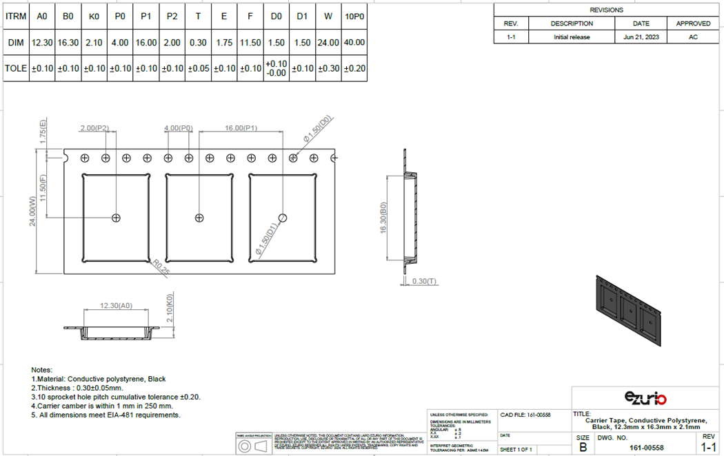
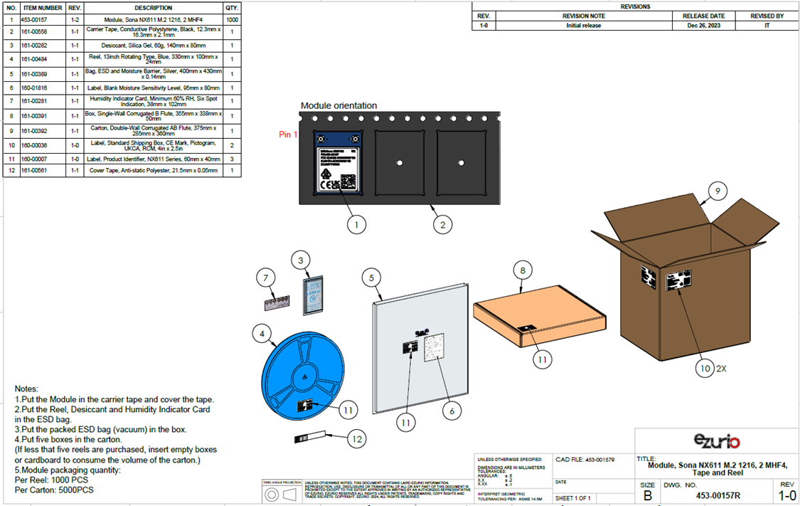
There are 1,000 SONA™NX61X SIP modules taped in a reel (and packaged in a pizza box) and five boxes per carton (5,000 modules per carton). Reel, boxes, and carton are labeled with the appropriate labels.

Base 1216 Module Shipping
There are 1,000 SONA™NX61X 1216 modules taped in a reel (and packaged in a pizza box) and five boxes per carton (5,000 modules per carton). Reel, boxes, and carton are labeled with the appropriate labels.
Base 2230 Module Shipping
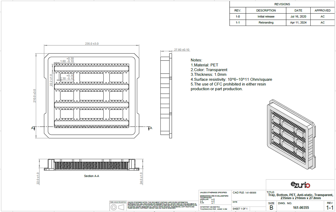
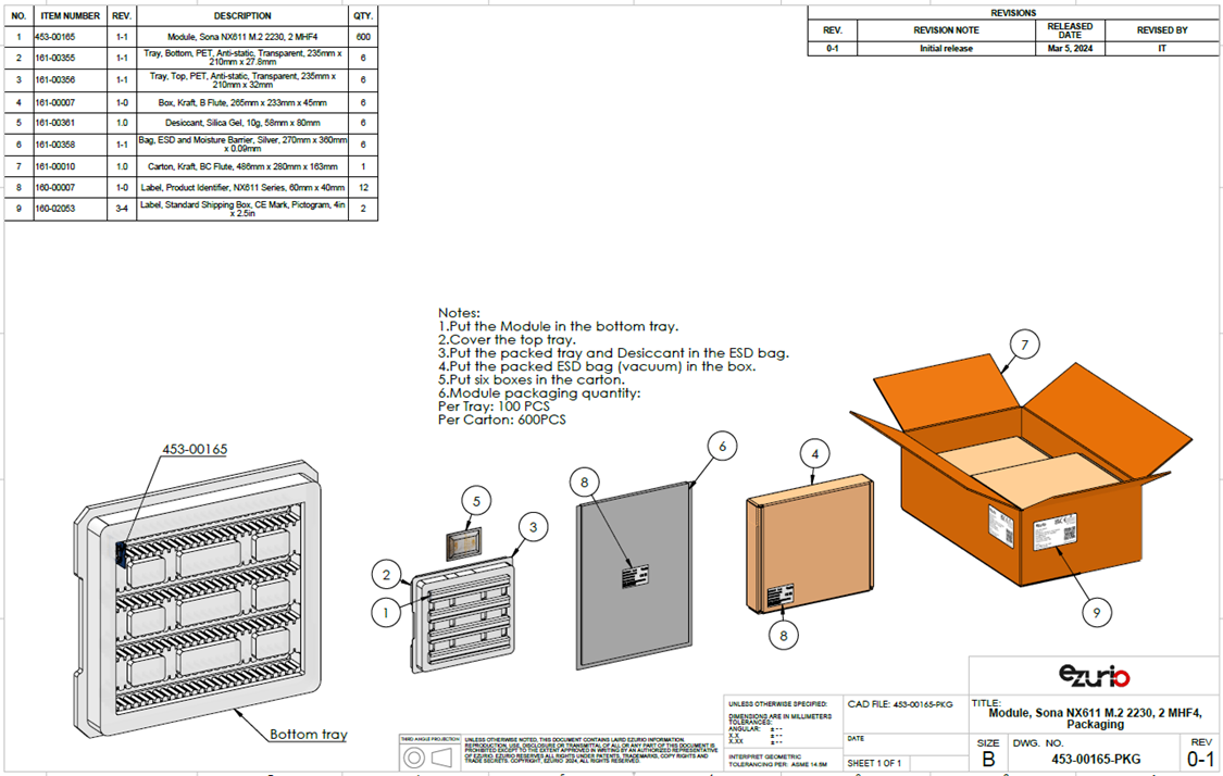
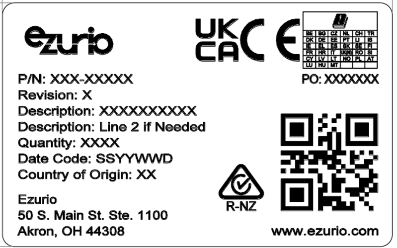
Labeling
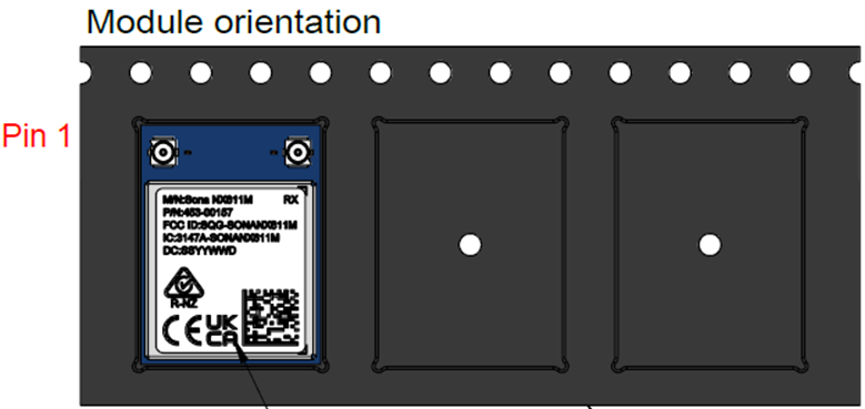
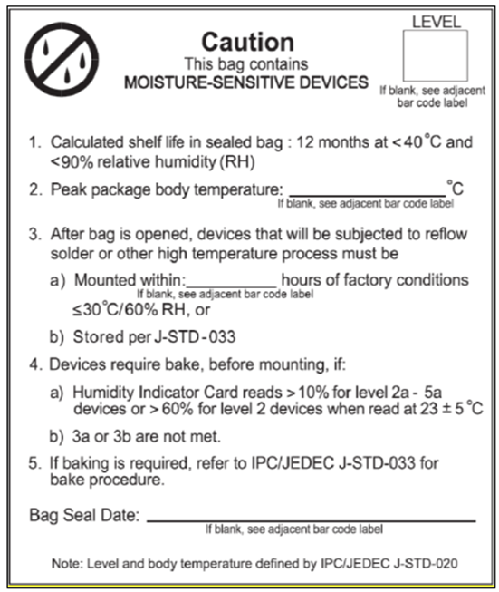
The following labels are located on the anti-static bag. Sona NX611 SIPs and 1216 modules are MSL4 modules.
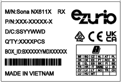
The following label is located on the pizza box.
The following package label is located on adjacent sides of the master carton.
Recommended Stencil Aperture
When soldering, the stencil thickness should be ≥ 0.1 mm.
Soldering
Note: When soldering, the stencil thickness should be ≥ 0.1 mm.
`Convection reflow or IR/Convection reflow (one-time soldering or two-time soldering in air or nitrogen environment)
- Measuring point – IC package surface
Temperature profile:
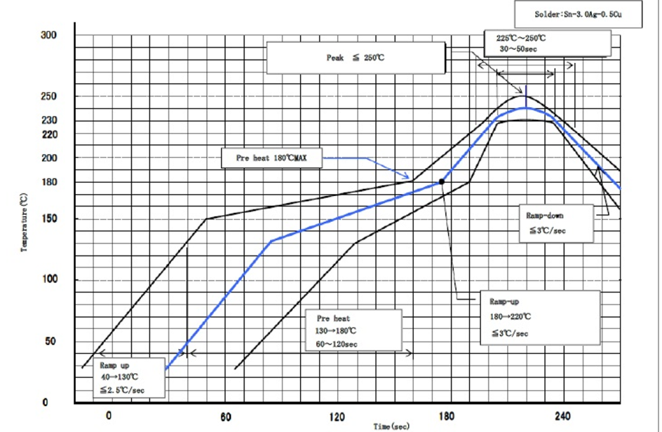
- Ramp-up: 40-130˚C. Less than 2.5˚C/sec
- Pre heat: 130-180˚C 60-120 sec, 180˚C MAX
- Ramp-up: 180-220˚C. Less than 3˚C/sec
Peak Temperature: MAX 250˚C
- 225˚C ~ 250˚C, 30 ~ 50 sec
- Ramp-down: Less than 3˚C/sec
Cautions when Removing the SIP from the Platform for RMA
- Bake the platform PCBA before removing the SIP module from the platform.
- Remove the SIP module by using a hot air gun. This process should be carried out by a skilled technician.
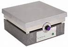
Recommended conditions for one-side component platform:
- Set the hot plate at 280°C.
- Put the platform on the hot plate for 8~10 seconds.
- Remove the device from platform.
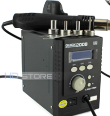
Recommended conditions for two-side components platform:
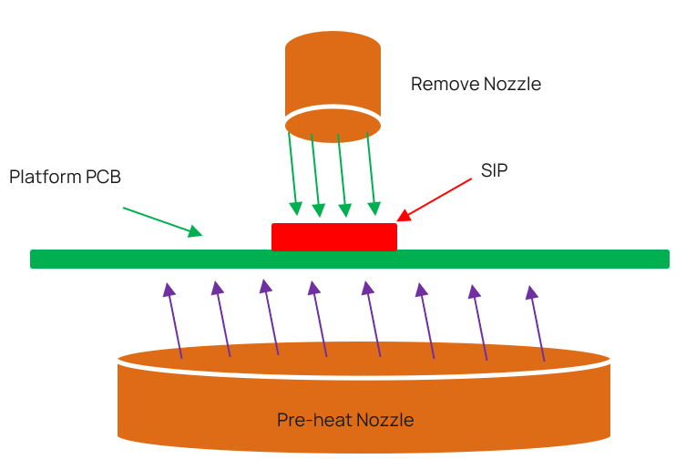
- Use two hot air guns.
- On the bottom, use a pre-heated nozzle (temp setting of 200~250°C) at a suitable distance from the platform PCB.
On the top, apply a remove nozzle (temp setting of 330°C). Heat until device can be removed from platform PCB.
- Remove the residue solder under the bottom side of device. (Note: Alternate module pictured as an example)
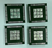 |  |
| (Not accepted for RMA) | (Accepted for RMA analysis) |
- Remove and clean the residue flux as needed.
Precautions for Use
- Opening/handing/removing must be done on an anti-ESD treated workbench. All workers must also have undergone anti-ESD treatment.
- The devices should be mounted within one year of the date of delivery.
- The SONA™NX61X SIP and 1216 modules are MSL level 4.
- The SONA™NX61X M2 modules are MSL level 1.
Environmental and Reliability
Environmental Requirements
Required Storage Conditions
Prior to Opening the Dry Packing
The following are required storage conditions prior to opening the dry packing:
- Normal temperature: 5~40˚C
- Normal humidity: 80% (Relative humidity) or less
- Storage period: One year or less
Note: Humidity means relative humidity.
After Opening the Dry Packing
The following are required storage conditions after opening the dry packing (to prevent moisture absorption):
Storage conditions for one-time soldering:
- Temperature: 5-25°C
- Humidity: 60% or less
- Period: 72 hours or less after opening
Storage conditions for two-time soldering
Storage conditions following opening and prior to performing the 1st reflow:
- Temperature: 5-25°C
- Humidity: 60% or less
- Period: A hours or less after opening
Storage conditions following completion of the 1st reflow and prior to performing the 2nd reflow
- Temperature: 5-25°C
- Humidity: 60% or less
- Period: B hours or less after completion of the 1st reflow
Note: Should keep A+B within 72 hours.
Temporary Storage Requirements after Opening
The following are temporary storage requirements after opening:
- Only re-store the devices once prior to soldering.
- Use a dry box or place desiccant (with a blue humidity indicator) with the devices and perform dry packing again using vacuumed heat-sealing.
The following indicate the required storage period, temperature, and humidity for this temporary storage:
Storage temperature and humidity:
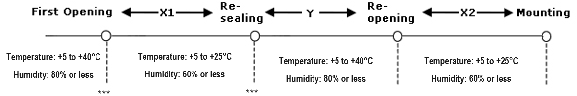
*** - External atmosphere temperature and humidity of the dry packing
Storage period:
- X1+X2 – Refer to Material handling information
- Required Storage Conditions. Keep is X1+X2 within 72 hours.
- Y – Keep within two weeks or less.
Baking Conditions
Baking conditions and processes for the module follow the J-STD-033 standard which includes the following:
- The calculated shelf life in a sealed bag is 12 months at <40℃ and <80% relative humidity.
- Once the packaging is opened, the SiP must be mounted (per MSL4/Moisture Sensitivity Level 4) within 72 hours at <30˚C and <60% relative humidity.
If the SiP is not mounted within 72 hours or if, when the dry pack is opened, the humidity indicator card displays >10% humidity, then the product must be baked for 48 hours at 125 ˚C (±5 ˚C).
Reliability Tests
Climatic and Dynamic
| Test Item | Specification | Standard | Test Result |
|---|---|---|---|
| Thermal Shock | Temperature: -40 ~ 85℃ Ramp time: Less than 10 seconds. Dwell Time: 10 minutes Number of Cycles: 350 times | *JESD22-A106 *IEC 60068-2-14 for dwell time and number of cycles | Pass |
| Vibration Non-operating Unpackaged device | Vibration Wave Form: Sine Waveform Vibration frequency / Displacement: 20-80 Hz/1.5mm Vibration frequency / Acceleration: 80-2000 Hz/20g Cycle Time: 4 min/cycle Number of Cycles: 4 cycle/axis Vibration Axes:X, Y and Z (Rotate each axis on vertical vibration table) | JEDEC 22-B103B (2016) | Pass |
| Mechanical Shock Non-operating Unpackaged device | Pulse shape: Half-sine waveform Impact acceleration: 1500 g Pulse duration: 0.5 ms Number of shocks: 30 shocks (5 shocks for each face) Orientation: Bottom, top, left, right, front and rear faces | JEDEC 22-B110B.01 (2019) | Pass |
Reliability Prediction
| Ezurio Part Number | Environment | Standard | Test Result 45 ℃ (Hours) |
|---|---|---|---|
| 453-00155R 453-00155C 453-00156R 453-00156C | Ground, Fixed, Uncontrolled | Telcordia Issue 3 | 4,020,768 |
| 453-00157R 453-00157C 453-00158R 453-00158C | Ground, Fixed, Uncontrolled | Telcordia Issue 3 | 2,668,324 |
| 453-00165 453-00166 | Ground, Fixed, Uncontrolled | Telcordia Issue 3 | 3,600,089 |
| 453-00155R 453-00155C 453-00156R 453-00156C | Mobile, Fixed, Uncontrolled | Telcordia Issue 3 | 1,507,788 |
| 453-00157R 453-00157C 453-00158R 453-00158C | Mobile, Fixed, Uncontrolled | Telcordia Issue 3 | 1,000,622 |
| 453-00165 453-00166 | Mobile, Fixed, Uncontrolled | Telcordia Issue 3 | 1,350,033 |
| Ezurio Part Number | Environment | Standard | Test Result 85 ℃ (Hours) |
|---|---|---|---|
| 453-00155R 453-00155C 453-00156R 453-00156C | Ground, Fixed, Uncontrolled | Telcordia Issue 3 | 865,986 |
| 453-00157R 453-00157C 453-00158R 453-00158C | Ground, Fixed, Uncontrolled | Telcordia Issue 3 | 567,761 |
| 453-00165 453-00166 | Ground, Fixed, Uncontrolled | Telcordia Issue 3 | 772,686 |
| 453-00155R 453-00155C 453-00156R 453-00156C | Mobile, Fixed, Uncontrolled | Telcordia Issue 3 | 324,745 |
| 453-00157R 453-00157C 453-00158R 453-00158C | Mobile, Fixed, Uncontrolled | Telcordia Issue 3 | 210,660 |
| 453-00165 453-00166 | Mobile, Fixed, Uncontrolled | Telcordia Issue 3 | 289,757 |
Regulatory, Qualification & Certifications
Regulatory Approvals
Note: For complete regulatory information, refer to the SONA™ NX61X Regulatory Information document (coming soon) which is also available from the SONA™ NX61X product page.
SONA™NX61X countries with certification (SIP)
| Country/Region | Regulatory ID |
|---|---|
| USA (FCC) | SQG-SONANX611S |
| EU | N/A |
| Canada (ISED) | 3147A-SONANX611S |
| Japan (MIC) | TBD |
| Australia | N/A |
| New Zealand | N/A |
SONA™NX61X countries with certification (M.2 1216 Module and M.2 2230 Module)
| Country/Region | Regulatory ID |
|---|---|
| USA (FCC) | SQG-SONANX611M |
| EU | N/A |
| Canada (ISED) | 3147A-SONANX611M |
| Japan (MIC) | TBD |
| Australia | N/A |
| New Zealand | N/A |
Certified Antennas
| Manufacturer | Model | Ezurio Part Number | Type | Connector | Peak Gain (dBi) 2.4 GHz | Peak Gain (dBi) 5 GHz | Peak Gain (dBi) 6 GHz |
|---|---|---|---|---|---|---|---|
| Ezurio (Laird Connectivity) | FlexMIMO 6E | EFD2471A3S-10MH4L | PIFA | MHF4L | 2.2 | 3.8 | 3.3 |
| Ezurio (Laird Connectivity) | FlexPIFA 6E | EFB2471A3S-10MH4L | PIFA | MHF4L | 2.2 | 3.9 | 3.8 |
| Ezurio (Laird Connectivity) | Mini NanoBlade Flex 6 GHz | EMF2471A3S-10MH4L | PCB Dipole | MHF4L | 2.4 | 4.4 | 5.2 |
| Joymax Inc. | Dipole 6E | TWX-100BRS3B | Dipole | RP-SMA | 2.0 | 4.0 | 4.0 |
| Ezurio (Laird Connectivity) | Dual Band FlexPIFA | 001-0021 | PIFA | MHF4L | 2.5 | 3.0 | N/A |
| TDK | Multilayer Antenna | ANT162442DT-2001A2 | Chip Antenna | N/A | 2.0 | 1.0 | N/A |
Bluetooth SIG Qualification
The Bluetooth Qualification Process promotes global product interoperability and reinforces the strength of the Bluetooth® brand and ecosystem to the benefit of all Bluetooth SIG members. The Bluetooth Qualification Process helps member companies ensure their products that incorporate Bluetooth technology comply with the Bluetooth Patent & Copyright License Agreement and the Bluetooth Trademark License Agreement (collectively, the Bluetooth License Agreement) and Bluetooth Specifications.
The Bluetooth Qualification Process is defined by the Qualification Program Reference Document (QPRD) v3.
To demonstrate that a product complies with the Bluetooth Specification(s), each member must for each of its products:
- Identify the product, the design included in the product, the Bluetooth Specifications that the design implements, and the features of each implemented specification
- Complete the Bluetooth Qualification Process by submitting the required documentation for the product under a user account belonging to your company
The Bluetooth Qualification Process consists of the phases shown below:

To complete the Qualification Process the company developing a Bluetooth End Product shall be a member of the Bluetooth SIG. To start the application please use the following link: Apply for Adopter Membership
Scope
This guide is intended to provide guidance on the Bluetooth Qualification Process for End Products that reference multiple existing designs, that have not been modified, (refer to Section 3.2.2.1 of the Qualification Program Reference Document v3).
For a Product that includes a new Design created by combining two or more unmodified designs that have DNs or QDIDs into one of the permitted combinations in Table 3.1 of the QPRDv3, a Member must also provide the following information:
- DNs or QDIDs for Designs included in the new Design
- The desired Core Configuration of the new Design (if applicable, see Table 3.1 below)
- The active TCRL Package version used for checking the applicable Core Configuration (including transport compatibility) and evaluating test requirements
Any included Design must not implement any Layers using withdrawn specification(s).
When creating a new Design using Option 2a, the Inter-Layer Dependency (ILD) between Layers included in the Design will be checked based on the latest TCRL Package version used among the included Designs.
For the purposes of this document, it is assumed that the member is combining unmodified Core-Controller Configuration and Core-Host Configuration designs, to complete a Core-Complete Configuration.
Qualification Steps When Referencing multiple existing designs, (unmodified) – Option 2a in the QPRDv3
For this qualification option, follow these steps:
- To start a listing, go to: https://qualification.bluetooth.com/
- Select Start the Bluetooth Qualification Process.
Product Details to be entered:
- Project Name (this can be the product name or the Bluetooth Design name).
- Product Description
- Model Number
- Product Publication Date (the product publication date may not be later than 90 days after submission)
- Product Website (optional)
- Internal Visibility (this will define if the product will be visible to other users prior to publication)
- If you have multiple End Products to list then you can select ‘Import Multiple Products’, firstly downloading and completing the template, then by ‘Upload Product List’. This will populate Qualification Workspace with all your products.
Specify the Design:
- Do you include any existing Design(s) in your Product? Answer Yes, I do.
- Enter the multiple DNs or QDIDs used in your, (for Option 2a two or more DNs or QDIDs must be referenced)
- Select ‘I’m finished entering DN’s
- Once the DNs or QDIDs are selected they will appear on the left-hand side, indicating the layers covered by the design (should show Core-Controller and Core Host Layers covered).
- What do you want to do next? Answer, ‘Combine unmodified Designs’.
- The Qualification Workspace Tool will indicate that a new Design will be created and what type of Core-Complete configuration is selected.
- An active TCRL will be selected for the design.
- Perform the Consistency Check, which should result in no inconsistencies
- If there are any inconsistencies these will need to be resolved before proceeding
- Save and go to Test Plan and Documentation
Test Plan and Documentation
- As no modifications have been made to the combined designs the tool should report the following message:
‘No test plan has been generated for your new Design. Test declarations and test reports do not need to be submitted. You can continue to the next step.’ - Save and go to Product Qualification fee
- As no modifications have been made to the combined designs the tool should report the following message:
Product Qualification Fee:
- It’s important to make sure a Prepaid Product Qualification fee is available as it is required at this stage to complete the Qualification Process.
- Prepaid Product Qualification Fee’s will appear in the available list so select one for the listing.
- If one is not available select ‘Pay Product Qualification Fee’, payment can be done immediately via credit card, or you can pay via Invoice. Payment via credit will release the number immediately, if paying via invoice the number will not be released until the invoice is paid.
- Once you have selected the Prepaid Qualification Fee, select ‘Save and go to Submission’
Submission:
- Some automatic checks occur to ensure all submission requirements are complete.
- To complete the listing any errors must be corrected
- Once you have confirmed all design information is correct, tick all of the three check boxes and add your name to the signature page.
- Now select ‘Complete the Submission’.
- You will be asked a final time to confirm you want to proceed with the submission, select ‘Complete the Submission’.
- Qualification Workspace will confirm the submission has been submitted. The Bluetooth SIG will email confirmation once the submission has been accepted, (normally this takes 1 working day).
Download Product and Design Details (SDoC):
- You can now download a copy of the confirmed listing from the design listing page and save a copy in your Compliance Folder
For further information, please refer to the following webpage:
https://www.bluetooth.com/develop-with-bluetooth/qualification-listing/
Example Design Combinations
The following gives an example of a design possible under option 2a:
Ezurio Controller Subsystem + BlueZ 5.50 Host Stack (Ezurio Sona NX611 based design)
| Design Name | Owner | Declaration ID | QD ID | Link to listing on the SIG website |
|---|---|---|---|---|
| Sona NX611 | Ezurio | D069010 | 223670 | https://qualification.bluetooth.com/ListingDetails/220312 |
| BlueZ 5.50 Host Stack | Ezurio | D046330 | 138224 | https://qualification.bluetooth.com/ListingDetails/93911 |
Qualify More Products
If you develop further products based on the same design in the future, it is possible to add them free of charge. The new product must not modify the existing design i.e add ICS functionality, otherwise a new design listing will be required.
To add more products to your design, select ‘Manage Submitted Products’ in the Getting Started page, Actions, Qualify More Products. The tool will take you through the updating process.
Ordering Information
| Part Number | Description |
|---|---|
| 453-00155R | Module, Sona NX611 SIP, 2 RF Trace Pin, Tape and Reel |
| 453-00155C | Module, Sona NX611 SIP, 2 RF Trace Pin, Cut Tape |
| 453-00156R | Module, Sona NX611 SIP, 1 RF Trace Pin, Tape and Reel |
| 453-00156C | Module, Sona NX611 SIP, 1 RF Trace Pin, Cut Tape |
| 453-00157R | Module, Sona NX611 M.2 1216, 2 MHF4, Tape and Reel |
| 453-00157C | Module, Sona NX611 M.2 1216, 2 MHF4, Cut Tape |
| 453-00158R | Module, Sona NX611 M.2 1216, 1 MHF4, Tape and Reel |
| 453-00158C | Module, Sona NX611 M.2 1216, 1 MHF4, Cut Tape |
| 453-00165 | Module, Sona NX611 M.2 2230, 2 MHF4 |
| 453-00166 | Module, Sona NX611 M.2 2230, 1 MHF4 |
| 453-00155-K1 | Development Kit, Module, Sona NX611 SIP, 2 RF Trace Pin |
| 453-00156-K1 | Development Kit, Module, Sona NX611 SIP, 1 RF Trace Pin |
| 453-00165-K1 | Development Kit, Module, Sona NX611 M.2 2230, 2 MHF4 |
| 453-00166-K1 | Development Kit, Module, Sona NX611 M.2 2230, 1 MHF4 |
Legacy - Revision History
| Version | Date | Notes | Contributors | Approver |
|---|---|---|---|---|
| 0.1 | 23 March 2023 | Preliminary version | PGS | Andy Ross |
| 0.2 | 04 June 2024 | Updated RF Characteristics | Brian Petted | Andy Ross |
| 0.3 | 14 June 2024 | Added Additional Pin Information. Moved Mechanical Specs. | PGS | Andy Ross |
| 0.4 | 02 July 2024 | Added Additional Pin Definitions. Removed 1218 Info. | PGS | Andy Ross |
| 0.5 | 11 Nov 2024 | Corrected supply domain parameter in Table 4, M.2 2230 Pin Definition for Pin 54 and Pin 20. Added Bluetooth Qualification Process. | Seokwoo Yoon Peter Scharpf | Dave Drogowski |
| 1.0 | 3 Feb 2025 | Initial release. | Peter Scharpf | Andy Ross |
| 1.1 | 11 Feb 2025 | Corrected 453-00157 description to reflect 2 antenna connectors in General Description | Dave Drogowski | Andy Ross |
| 1.2 | 20 May 2025 | Removed DFW Radar pulse detection from 6.1 IEEE 802.11 standards | Dave Drogowski | Andy Ross |