/filters:background_color(white)/2025-01/453-00219%20front4.416.png)
Introduction
Overview
This document describes key hardware aspects of the Veda SL917 NCP Module. This document is intended to assist device manufacturers and related parties with the integration of this radio into their host devices. Data in this document is drawn from several sources. For full documentation on the Veda SL917, visit:
https://www.ezurio.com/veda-sl917
General Description
Ezurio’s SL917 Network Co-Processor Connectivity module is based on the Silicon Labs SiWN917M, which is our lowest power Wi-Fi 6 silicon, ideal for ultra-low power IoT wireless devices using Wi-Fi®, Bluetooth, and IP networking for secure cloud connectivity. It has an integrated built-in wireless subsystem, advanced security, and integrated power- management. It has a multi-threaded Network Wireless Processor (NWP) running up to 160 MHz. All the networking and wireless stacks run on independent threads of the multi-threaded processor. The SL917 includes an ultra-low power Wi-Fi 6 plus Bluetooth Low Energy (LE) 5.4 wireless CPU subsystem, baseband digital signal processing, analog front end, 2.4 GHz RF transceiver and integrated power amplifier, embedded SRAM, FLASH and power management subsystem all in a single 16 x 21.1 x 2.3 mm PCB module package thus providing a fully integrated solution that is ready for a wide range of embedded wireless IoT applications. The SL917 module is a complete solution offered with robust and fully-upgradeable software stacks, global regulatory certifications, advanced development and debugging tools, and documentation that simplifies and minimizes the development cycle of your end-product, helping to accelerate its time-to-market. The modules come with modular radio type approvals for various countries, including USA (FCC), Canada (IC/ISED) and Japan (MIC), and are in compliance with the relevant EN standards (including EN 300 328 v2.2.2) for the conformity with the directives and regulations in EU and UK.
This datasheet is subject to change. Please contact Ezurio for further information.
Application Areas
- Smart Home
- Security Cameras
- HVAC
- Smart Sensors
- Smart Appliances
- Health and Fitness
- Pet Tracker
- Smart Cities
- Smart Meters
- Industrial Wearable
- Smart Buildings
- Asset Tracking
- Smart hospitals
Features & Benefits
The Veda SL917 NCP module features and benefits are described below.
- Wi-Fi 6 Single Band 2.4 GHz 20MHz 1x1 stream IEEE 802.11 b/g/n/ax
- Bluetooth LE 5.4
- Wi-Fi 6 Benefits: TWT for improved efficiency and longer battery life, MU- MIMO/OFDMA for Higher Throughput, network capacity and low latency
- Best in Class Device and Wireless Security
- WLAN Tx power up to +17.5 dBm with integrated PA
- Bluetooth LE Tx power up to +17 dBm with integrated PA
- WLAN Rx sensitivity as low as -95 dBm
- Wi-Fi Standby Associated mode current: 78 μA @ 1-second beacon listen interval
- In-package Flash up to 4MB,
- Embedded Wi-Fi, Bluetooth LE and networking stacks supporting wireless coexistence
- Operating temperature: -40 ºC to +85 ºC
- Operating supply range: 3.0 V - 3.63 V
- Supply voltage for GPIOs: 1.71 V to 3.63 V
Specification Summary
Processor / SoC / Chipset
| Wireless | Silicon Labs SiWN917M |
Wi-Fi
| Standards | Wi-Fi 6 (802.11 b/g/n/ax) |
| Wi-Fi Features |
|
| Frequency Range |
|
| Spatial Streams |
|
| Channel Support |
|
| Supported Data Rates |
|
| Max Transmit Power |
|
| Receive Sensitivity |
|
| Operating Modes |
|
| Wi-Fi Stack | Embedded Wi-Fi Stack1
|
| Coexistence |
|
Bluetooth
| Standards | Bluetooth® LE 5.4 |
| Bluetooth Features |
|
| Frequency Range |
|
| Max Transmit Power |
|
| Receive Sensitivity |
|
| Bluetooth Stack | Embedded Bluetooth Stack
|
Radio Performance
| Miscellaneous |
|
Interfaces
| Physical Interfaces | SMT Module |
| Memory Interfaces |
|
Power
| Input Voltage |
|
| GPIO Supply Voltage |
|
| Wireless Sub-System Power Consumption |
|
| Power Management |
|
Mechanical
| Dimensions | 21.10 x 16 x 2.32 mm |
Software
| Security |
|
Environmental
| Operating Temperature |
|
| Lead Free | Lead-free and RoHS Compliant |
Certifications
| Regulatory Compliance | FCC (USA) IC/ISED (Canada) CE (EU) UKCA (UK) MIC (Japan) KC (South Korea) NCC (Taiwan) SRRC (China) ACMA (Australia) RSM (New Zealand)3 |
| Bluetooth SIG | Bluetooth SIG Qualification3 |
| Wi-Fi Alliance | Wi-Fi 43, Wi-Fi 63 |
Development
| Development Kit | MIKROE-6488 Click Board- SL917 Click External/Trace Antenna Click Board |
Warranty
| Warranty Terms | One Year Warranty |
Notes:
Note1: For a detailed list of software features and available profiles, refer to the Software Reference Manuals or contact Ezurio for availability.
Note2: All power and performance numbers are under ideal conditions.
Note3: For information about Software roadmap features and additional certification information, contact Ezurio for availability and timeline. Currently, we have certifications for FCC (USA), IC/ISED (Canada), CE (EU), UKCA (UK), MIC (Japan), ACMA (Australia), RSM (New Zealand), but not yet for KC (South Korea), NCC (Taiwan), SRRC (China). These last three are pending.
Functional Descriptions
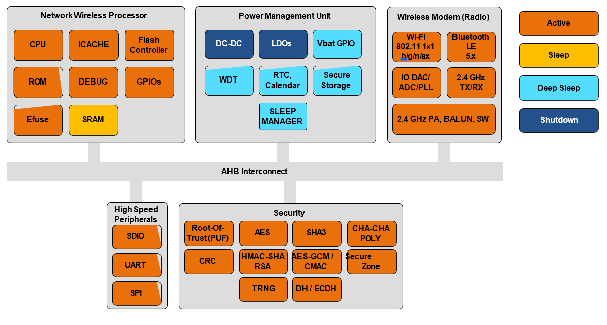
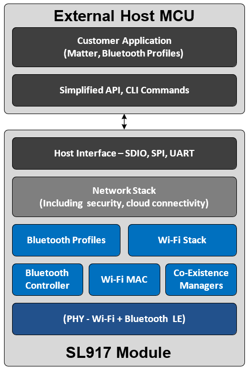
An SL917 module running the NCP mode of operation includes a Network Wireless Processor (NWP) 4-Threaded processor running up to 160 MHz. All the networking and wireless stacks run on independent threads of the NWP. In addition, the NWP subsystem also acts as the secure processing domain and takes care of secure boot, secure firmware update and provides access to security accelerators and secure peripherals through pre-defined APIs. The NWP based "Networking, Security and Wireless subsystem" have power, clocks/ PLLs, bus-matrices, and memory.
WLAN Functional Description
- Compliant to single-spatial stream IEEE 802.11 b/g/n/ax with single band (2.4 GHz) support
- Support for 20 MHz channel bandwidth for 802.11n and 802.11ax.
- Operating Modes: Wi-Fi 4 STA, Wi-Fi 6 (802.11ax) STA, Wi-Fi 4 AP, Enterprise STA, Wi-Fi 6 STA + Wi-Fi 4 AP, Wi-Fi + BLE
- Wi-Fi 6 Features: Individual Target wake-up time (iTWT), Broadcast TWT (bTWT),SU extended range (ER), DCM (Dual Carrier Modulation), DL MU-MIMO, DL/UL OFDMA, MBSSID, BFRP, Spatial Re-use, BSS Coloring, and NDP feedback up to 4 antennas
- Integrated PA
- Data Rates—802.11b: up to 11 Mbps; 802.11g: up to 54 Mbps; 802.11n: MCS0 to MCS7; 802.11ax: MCS0 to MCS7
- Operating Frequency Range [MHz]: 2412-2462 (North America, default), 2412-2472 (Europe, and other countries where applicable), 2412-2484 (Japan)
MAC
- Conforms to IEEE 802.11b/g/n/ax standards for MAC
- Hardware accelerators for AES
- WPA, WPA2, WPA3 and WMM support
- AMPDU aggregation for high performance
- Firmware downloaded from host based on application
- Hardware accelerators for DH (for WPS) and ECDH
Baseband Processing
- Supports 11b: DSSS for 1, 2 Mbps and CCK for 5.5, 11 Mbps
Supports all OFDM data rates:
- 802.11g: 6, 9, 12, 18, 24, 36, 48, 54 Mbps
- 802.11ax, 802.11n: MCS 0 to MCS 7
- High-performance multipath handling in OFDM, DSSS, and CCK modes
Bluetooth Functional Description
- Transmit power up to +17 dBm with integrated PA
- Receive sensitivity — LE: -93 dBm, LR 125 Kbps: -104.5 dBm
- Operating Frequency Range — 2.402 GHz - 2.480 GHz
- Supports Bluetooth® Low Energy (LE): High Speed (1 Mbps and 2 Mbps) and Long Range (LE Coded PHYs, 125 Kbps and 500 Kbps)
- Advertising extensions
- Data length extensions
- LL privacy
- LE dual role
- BLE acceptlist
- Two simultaneous BLE connections (2 peripheral or 2 central, or 1 central and 1 peripheral)
MAC
Link Manager
- Creation, modification & release of physical links
- Connection establishment between Link managers of two Bluetooth devices
- Link supervision is implemented in Link Manager
- Link power control is done depending on the inputs from Link Controller
- Enabling & disabling of encryption & decryption on logical links
- AES hardware acceleration
Link Controller
- Encodes and decodes header of BLE packets
- Manages flow control, acknowledgment, re-transmission requests, etc.
- Stores the last packet status for all physical transports
- Indicates the success status of packet transmission to upper layers
- Indicates the link quality to the LMP layer
Device Manager
- Executes HCI Commands
- Controls Scan & Connection processes
- Controls all BLE Device operations except data transport operations
- BLE Controller state transition management
- Anchor point synchronization & management
- Scheduler
Baseband Processing
- Supports BLE 1Mbps, 2Mbps and long range 125kbps, 500kbps
RF Transceiver
- The SL917 features two highly configurable RF transceivers supporting WLAN 11b/g/n/ax and Bluetooth LE wireless protocols. Both RF transceivers together operating in multiple modes covering High Performance (HP) and Low Power (LP) operations. List of operating modes are given in next section.
- It contains two fully integrated fractional-N frequency synthesizers having reference from internal oscillator with 40 MHz crystal. One of the synthesizer is a low power architecture which also caters single-bit data modulation feature for Bluetooth LE protocols.
Receiver and Transmitter Operating Modes
The available radio operating modes are as follows:
- WLAN HP TX - WLAN High-Performance Transmitter
- WLAN HP RX - WLAN High-Performance Receiver
- WLAN LP RX - WLAN Low-Power Receiver
- BLE HP TX - Bluetooth LE High-Performance Transmitter
- BLE HP RX - Bluetooth LE High-Performance Receiver
- BLE LP TX - Bluetooth LE Low-Power Transmitter
- BLE LP RX - Bluetooth LE Low-Power Receiver
Note: All the TX / RX modes are automatically controlled by radio firmware and not individually selectable.
Security
- Secure Boot
- Secure OTA Firmware update
- TRNG : Generates high-entropy random numbers based on RF noise, increasing the effort/time needed to expose secret keys
- Secure Zone
- Secure Key storage : HW device identity and key storage with PUF
- Debug Lock
- Anti Rollback : Firmware downgrade to a lower version is prohibited through OTP to prevent the use of older, potentially vulnerable FW version
- Encrypted XIP from flash with XTS/CTR mode
- Secure Attestation : Allows a device to authenticate its identity using a cryptographically signed token and exchange of secret keys
- Hardware Accelerators: AES128/256/192, SHA256/384/512, HMAC, RNG, CRC, SHA3, AES-GCM/ CMAC, ChaCha-poly
- Software Implementation: RSA and ECC
Software & Firmware
Embedded Wi-Fi Software
- The wireless software package supports Embedded Wi-Fi (802.11 b/g/n/ax) Client mode, Wi-Fi Access point mode (up to 4 clients), and Enterprise Security in client mode.
- The software package includes complete firmware and application profiles.
- It has a wireless coexistence manager to arbitrate between protocols.
Embedded Wi-FI Software Security
Wireless software supports multiple levels of security capabilities available for the development of IoT devices.
- Accelerators: AES128/256
- WPA/WPA2/WPA3-Personal, WPA/WPA2/WPA3 Enterprise for Client
Power
Power Architecture
The Power Control Hardware implements the control sequences for transitioning between different power states (Active/Standby/Sleep/ Shutdown).
Highlights
- Two integrated buck switching regulators (High performance and ULP) to enable efficient Voltage Scaling across wide operating mode currents ranging from <1 μA to 250 mA
- Multiple voltage domains with Independent voltage scaling of each domain.
- Fine grained power-gating including peripherals, buses and pads, thereby reducing power consumption when the peripheral/buses/ pads are inactive.
- Flexible switching between different Active states with controls from Software.
- Hardware based wakeup from Standby/Sleep/Shutdown states.
- All the peripherals are clock gated by default thereby reducing the power consumption in inactive state.
- Low wakeup times as configurable by Software.
Power Management
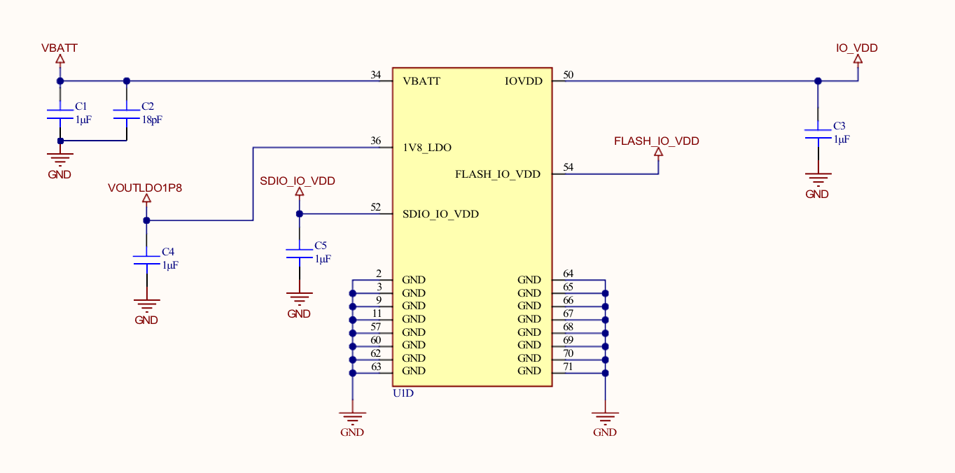
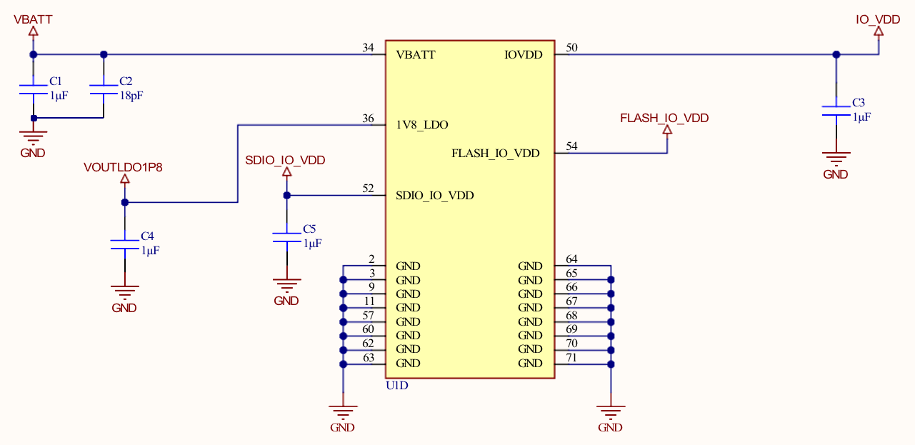
The SL917 NCP modules have an internal power management subsystem, including DC-DC converters and linear regulators. This subsystem generates all the voltages required by the module to operate from a wide variety of input sources.
- Input voltage (3.3 V) on pin VBATT
- Input voltage (1.8 V or 3.3 V) on pin IO_VDD, SDIO_IO_VDD and ULP_IO_VDD
- Input voltage (1.8 V) on pin FLASH_IO_VDD
- Nominal Output - 1.8 V and 48 mA maximum load on pin 1V8_LDO
Power Modes
It supports Ultra-low power consumption with multiple power modes to reduce system energy consumption.
- Voltage and Frequency Scaling
- Deep sleep (ULP) mode with only the sleep timer active – with and without RAM retention
- Wi-Fi standby associated mode with automatic periodic wake-up
- Automatic clock gating of the unused blocks or transit the system from Normal to ULP mode.
ULP Mode
In Ultra Low Power mode, the deep sleep manager has control over the processors and subsystems and controls their active and sleep states. During deep sleep, the always-on logic domain operates on a lowered supply and a 32 kHz low-frequency clock to reduce power consumption. The ULP mode supports the following wake-up options:
- Timeout wakeup - Exit sleep state after programmed timeout value.
- GPIO Based Wakeup: Exit sleep state when GPIO goes High/Low based on programmed polarity.
Memory
Architecture
There are on chip Read Only Memory(ROM), Random Access Memory(RAM) and in-package flash connectivity. Sizes of ROM/RAM/ flash will vary depending on the chip configuration.
The NWP processor has the following memory:
- Embedded SRAM up to 672 KB total
- 448 KB of ROM which holds the Secure primary bootloader, Network Stack, Wireless stacks and security functions
- 16 KB of Instruction cache (I cache)
- Flash up to 4 MB (in-package)
- eFuse of 1024 bytes (used to store primary boot configuration, security and calibration parameters)
Hardware Architecture
Block Diagrams
Note: Customer can connect multiple hosts, but only one host interface can be active after power-on.
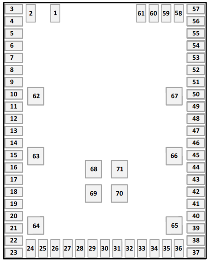
Pin-Out / Package Layout
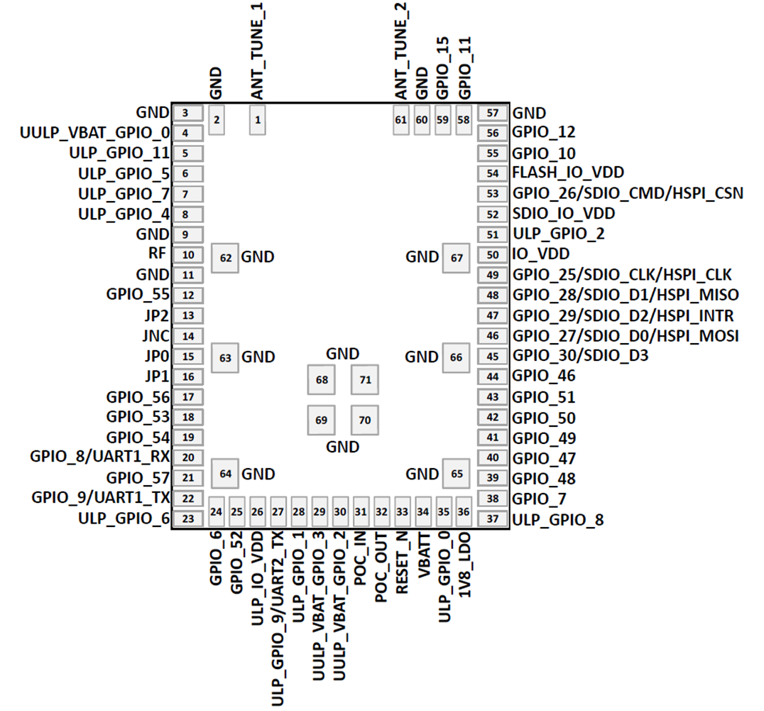
List of Pins in IC (SiWN917M), Not Available in the Modules
| Pin Name | QFN I/O Supply Domain | Direction | Initial State (Power up, Active Reset) | Description |
|---|---|---|---|---|
| RF_BLETX | RF_AVDD | Output | NA | BLE 8 dBm RF Output |
| ULP_GPIO_10 | ULP_IO_VDD | Inout | HighZ | Default: HighZ Sleep: HighZ |
| XTAL_32KHZ_P | NA | Inout | NA | Analog Pin. 32KHZ XTAL Connection |
| XTAL_32KHZ_N | NA | Inout | NA | Analog Pin. 32KHZ XTAL Connection |
| UULP_VBAT_GPIO_1 | VBATT | Inout | HighZ | Default: High Sleep: High |
RF and Control Interfaces
| Pin Name | Pin No. | I/O Supply Domain | Direction | Initial State (Power up Active Reset) | Description |
|---|---|---|---|---|---|
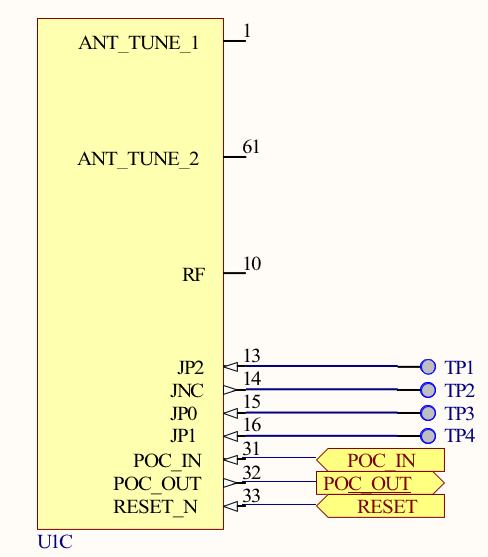
| ANT_TUNE_1 | 1 | N/A | Input | N/A | 453-00221: External fine-tuning option for the integral antenna; connect same tun- ing circuit on both ANT_TUNE1 and ANT_TUNE2 pins; leave floating if no fine- tuning is desired on the integral antenna; 453-00219: leave this pin floating |
| RF | 10 | VBATT | Inout | N/A | Connect to antenna with a 50-Ω impedance as per the reference schematics |
| POC_IN | 31 | VBATT | Input | NA | This is an input to the chip which resets all analog and digital blocks in the device. It should be made high only after supplies are valid. |
| POC_OUT | 32 | VBATT | Output | NA | This is internally generated. Initially, it is low. But it becomes high when the supply (VBATT) is valid. |
| RESET_N | 33 | VBATT | Inout | NA | Active-low reset asynchronous reset signal, which resets only digital blocks. RESET_N will be pulled low if POC_IN is low. |
| ANT_TUNE_2 | 61 | N/A | Input | N/A | 453-00221: External fine-tuning option for the integral antenna; connect same tun- ing circuit on both ANT_TUNE1 and ANT_TUNE2 pins; leave floating if no fine- tuning is desired on the integral antenna; 453-00219: leave this pin floating |
Power and Ground Pins
| Pin Name | Pin No. | Type | Direction | Description |
|---|---|---|---|---|
| ULP_IO_VDD | 26 | Power | Input | I/O supply for ULP I/Os. |
| VBATT | 34 | Power | Input | Power supply for the module. |
| 1V8_LDO | 36 | Power | Output | Output of 1.8V LDO which is used for Flash sup- ply. |
| IO_VDD | 50 | Power | Input | I/O Supply for GPIOs. Refer to GPIOs section for details on which GPIOs have this as the I/O supply. |
| SDIO_IO_VDD | 52 | Power | Input | I/O Supply for SDIO I/Os. Refer to GPIOs section for details on which GPIOs have this as the I/O supply. |
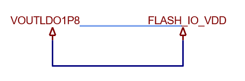
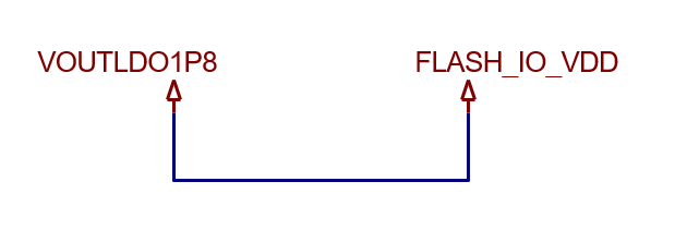
| FLASH_IO_VDD | 54 | Power | Input | I/O Supply for module embedded flash. Connect to 1V8_LDO as per Reference Schematics. |
| GND | 2, 3, 9, 11, 57, 60, 62-71 | Ground | Common ground pins. |
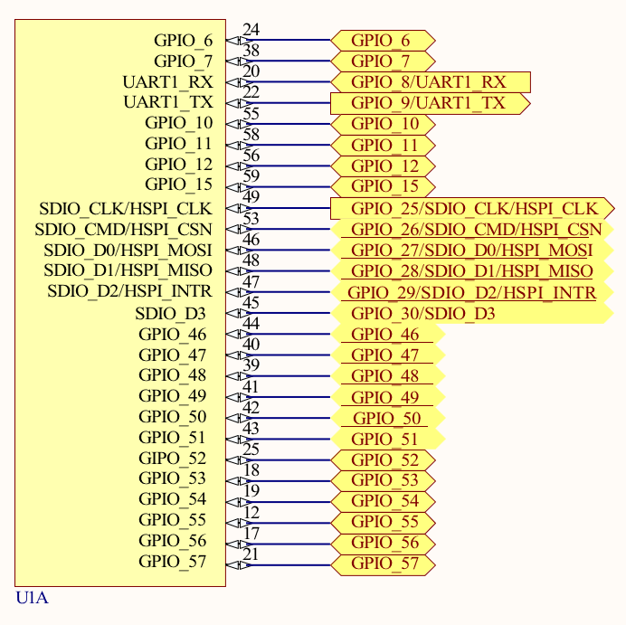
Peripheral Interfaces
| Pin Name | Pin No. | I/O Supply Domain | Direction | Initial State (Power up Active Reset) | Description | ||||||||||||
|---|---|---|---|---|---|---|---|---|---|---|---|---|---|---|---|---|---|
| UULP_VBAT_GPIO_0 | 4 | VBATT | Output | High | Default: High Sleep: High This pin can be configured by software to be any of the following.
| ||||||||||||
| ULP_GPIO_11 | 5 | ULP_IO_VDD | Inout | HighZ | Default: HighZ Sleep: HighZ | ||||||||||||
| ULP_GPIO_5 | 6 | ULP_IO_VDD | Inout | HighZ | Default: HighZ Sleep: HighZ | ||||||||||||
| ULP_GPIO_7 | 7 | ULP_IO_VDD | Inout | HighZ | Default: HighZ Sleep: HighZ | ||||||||||||
| ULP_GPIO_4 | 8 | ULP_IO_VDD | Inout | HighZ | Default: HighZ Sleep: HighZ | ||||||||||||
| GPIO_55 | 12 | IO_VDD | Inout | HighZ | Default: HighZ Sleep: HighZ | ||||||||||||
| JP2 | 13 | IO_VDD | Input | Pullup | Default: JP2 Sleep: HighZ JP2 - Reserved. Connect to a test point for debugging purposes | ||||||||||||
| JNC | 14 | IO_VDD | Output | Pullup | Default: JNC Sleep: HighZ JNC - Reserved. Connect to a test point for debugging purposes | ||||||||||||
| JP0 | 15 | IO_VDD | Input | Pullup | Default: JP0 Sleep: HighZ JP0 - Reserved. Connect to a test point for debugging purposes | ||||||||||||
| JP1 | 16 | IO_VDD | Input | Pullup | Default: JP1 Sleep: HighZ JP1 - Reserved. Connect to a test point for debugging purposes | ||||||||||||
| GPIO_56 | 17 | IO_VDD | Inout | HighZ | Default: HighZ Sleep: HighZ | ||||||||||||
| GPIO_53 | 18 | IO_VDD | Inout | HighZ | Default: HighZ Sleep: HighZ | ||||||||||||
| GPIO_54 | 19 | IO_VDD | Inout | HighZ | Default: HighZ Sleep: HighZ | ||||||||||||
| GPIO_8/UART1_RX | 20 | IO_VDD | Inout | HighZ |
| ||||||||||||
| GPIO_57 | 21 | IO_VDD | Inout | HighZ | Default: HighZ Sleep: HighZ | ||||||||||||
| GPIO_9/UART1_TX | 22 | IO_VDD | Inout | HighZ |
| ||||||||||||
| ULP_GPIO_6 | 23 | ULP_IO_VDD | Inout | HighZ | Default: HighZ Sleep: HighZ This pin can be configured by software to be any of the following.
| ||||||||||||
| GPIO_6 | 24 | IO_VDD | Inout | HighZ | Default: HighZ Sleep: HighZ | ||||||||||||
| GPIO_52 | 25 | IO_VDD | Inout | HighZ | Default: HighZ Sleep: HighZ | ||||||||||||
| ULP_GPIO_9/ UART2_TX | 27 | ULP_IO_VDD | Inout | HighZ | Default: UART2_TX- Debug UART Inter- face serial output Sleep: HighZ | ||||||||||||
| ULP_GPIO_1 | 28 | ULP_IO_VDD | Inout | HighZ | Default: HighZ Sleep: HighZ This pin can be configured by software to be any of the following
| ||||||||||||
| UULP_VBAT_GPIO_3 | 29 | VBATT | Inout | HighZ | Default: HighZ Sleep: EXT_32KHZ_IN This pin can be configured by software to be any of the following.
| ||||||||||||
| UULP_VBAT_GPIO_2 | 30 | VBATT | Inout | HighZ | Default: HighZ Sleep: ULP_WAKEUP This pin can be configured by software to be any of the following.
| ||||||||||||
| ULP_GPIO_0 | 35 | ULP_IO_VDD | Inout | HighZ | Default: HighZ Sleep: HighZ | ||||||||||||
| ULP_GPIO_8 | 37 | ULP_IO_VDD | Inout | HighZ | Default: HighZ Sleep: HighZ | ||||||||||||
| GPIO_7 | 38 | IO_VDD | Inout | HighZ | Default:HighZ Sleep: HighZ This pin can be configured by software to be any of the following. PTA_GRANT: "PTA Grant" output signal is part of 3-wire coexistence (Packet Traffic Arbitration) interface. | ||||||||||||
| GPIO_48 | 39 | IO_VDD | Inout | HighZ | Default: HighZ Sleep: HighZ | ||||||||||||
| GPIO_47 | 40 | IO_VDD | Inout | HighZ | Default: HighZ Sleep: HighZ | ||||||||||||
| GPIO_49 | 41 | IO_VDD | Inout | HighZ | Default: HighZ Sleep: HighZ | ||||||||||||
| GPIO_50 | 42 | IO_VDD | Inout | HighZ | Default: HighZ Sleep: HighZ | ||||||||||||
| GPIO_51 | 43 | IO_VDD | Inout | HighZ | Default: HighZ Sleep: HighZ | ||||||||||||
| GPIO_46 | 44 | IO_VDD | Inout | HighZ | Default: HighZ Sleep: HighZ | ||||||||||||
| GPIO_30/SDIO_D3 | 45 | SDIO_IO_VDD | Inout | Pullup |
| ||||||||||||
| GPIO_27/SDIO_D0/ HSPI_MOSI | 46 | SDIO_IO_VDD | Inout | HighZ |
| ||||||||||||
| GPIO_29/SDIO_D2/ HSPI_INTR | 47 | SDIO_IO_VDD | Inout | HighZ |
| ||||||||||||
| GPIO_28/SDIO_D1/ HSPI_MISO | 48 | SDIO_IO_VDD | Inout | HighZ |
| ||||||||||||
| GPIO_25/SDIO_CLK/ HSPI_CLK | 49 | SDIO_IO_VDD | Inout | HighZ |
| ||||||||||||
| ULP_GPIO_2 | 51 | ULP_IO_VDD | Input | HighZ | Default: HighZ Sleep:HighZ | ||||||||||||
| GPIO_26/SDIO_CMD/ SPI_CSN | 53 | SDIO_IO_VDD | Inout | HighZ |
| ||||||||||||
| GPIO_10 | 55 | IO_VDD | Inout | HighZ | Default: HighZ Sleep: HighZ This pin can be configured by software to be any of the following.
| ||||||||||||
| GPIO_12 | 56 | IO_VDD | Inout | HighZ | Default: HighZ Sleep: HighZ This pin can be configured by software to be any of the following.
| ||||||||||||
| GPIO_11 | 58 | IO_VDD | Inout | HighZ | Default: HighZ Sleep: HighZ This pin can be configured by software to be any of the following.
| ||||||||||||
| GPIO_15 | 59 | IO_VDD | Inout | HighZ | Default: HighZ Sleep: HighZ This pin can be configured by software to be any of the following.
|
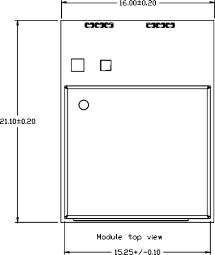
Mechanical Drawings
Dimensions
| Parameter | Value (LxWxH) | Units |
|---|---|---|
| Module Dimensions | 21.10 x 16 x 2.32 | mm |
| Tolerance | ±0.2 | mm |

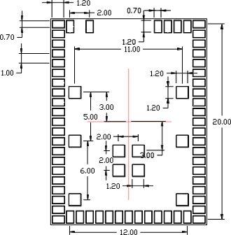
Pin Locations
Note: All coordinates in the following table are in millimeters, and in TOP VIEW.
| PAD X-Y Coordinates | |||
|---|---|---|---|
| Pad # | X | Y | Pad Size |
| 1 | -4 | 9.75 | (1.2 x 0.7) mm |
| 2 | -6 | 9.75 | |
| 3 | -7.2 | 10 | |
| 23 | -7.2 | -10 | |
| 24 | -6 | -9.75 | |
| 36 | 6 | -9.75 | |
| 37 | 7.2 | -10 | |
| 57 | 7.2 | -10 | |
| 58 | 6 | 9.75 | |
| 61 | 3 | 9.75 | |
| 62 | -5.5 | 3 | (1.2 x 1.2) mm |
| 63 | -5.5 | -2 | |
| 64 | -5.5 | -8 | |
| 65 | 5.5 | -8 | |
| 66 | 5.5 | -2 | |
| 67 | 5.5 | 3 | |
| 68 | -1 | -3 | |
| 69 | -1 | -5 | |
| 70 | 1 | -5 | |
| 71 | 1 | -3 | |
PCB Landing Pattern
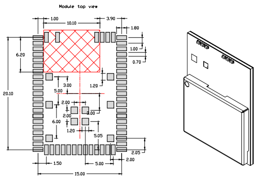
| PAD X-Y Coordinates | |||
|---|---|---|---|
| Pad # | X | Y | Pad Size |
| 1 | -4 | 10.05 | (1.8 x 0.7) mm |
| 2 | -6 | 10.05 | |
| 3 | -7.5 | 10 | |
| 23 | -7.5 | -10 | |
| 24 | -6 | -10.05 | |
| 36 | 6 | -10.05 | |
| 37 | 7.5 | -10 | |
| 57 | 7.5 | 10 | |
| 58 | 6 | 10.05 | |
| 61 | 3 | 10.05 | |
| 62 | -5.5 | 3 | (1.2 x 1.2) mm |
| 63 | -5.5 | -2 | |
| 64 | -5.5 | -8 | |
| 65 | 5.5 | -8 | |
| 66 | 5.5 | -2 | |
| 67 | 5.5 | 3 | |
| 68 | -1 | -3 | |
| 69 | -1 | -5 | |
| 70 | 1 | -5 | |
| 71 | 1 | -3 | |
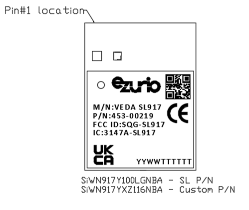
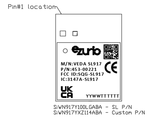
Module Marking Information
Schematics
Note:
Customers should include provision for programming or updating the firmware at manufacturing.
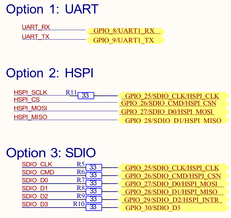
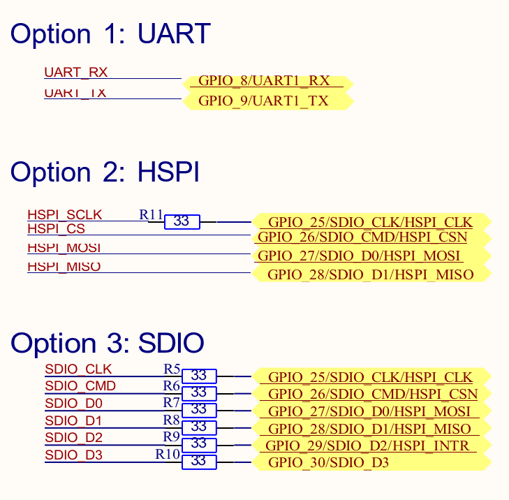
- If using UART, we recommend bringing out the SPI or SDIO lines to test points, so designers could use the faster interface for programming the firmware as needed.
- If using SPI or SDIO as host interface, then firmware programming or update can be done through the host MCU, or if design- er prefers to program standalone at manufacturing, then it is recommended to have test points on the SPI or SDIO signals.
- 3.3 V/1.8 V/VBATT must be supplied by external source.
- VBATT, SDIO_IO_VDD, IO_VDD, ULP_IO_VDD must be powered using External/On-board Power.
- FLASH_IO_VDD is powered by 1V8_LDO output.
- Place all the Caps closer to the corresponding Module pins.
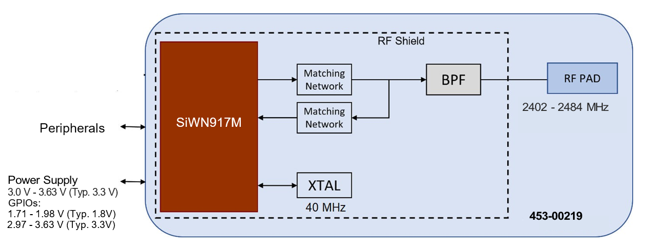
SL917 NCP Schematics for Parts with RF Pin
System Supplies
Notes:
- Place all the decoupling capacitors close to the module pins.
- IO_VDD, SDIO_IO_VDD, ULP_IO_VDD can be powered independently by different voltage sources based on their corresponding signals voltage levels requirements. Voltages must be as per Table 7.2 Recommended Operating Conditions on page 26.
- Even if GPIOs are not used, their respective IO domains must still be connected to the power supply.
RF, Debug, and Reset Connection
Notes:
- Place L1 close to the RF pin.
- It is mandatory to follow the reference schematics for optimal RF performance.
- Maintain 50 ohm characteristic impedance for RF traces.
- J1: In-built antenna or an external antenna (with RF connector) can be used.
- It is recommended to add microwave coaxial switch connector (Example : Murata's MM8430-2610RA1) or MHF4 connector for conducted measurements.
- Additional matching circuit to be provided near the antenna, based on antenna used and location on the board.
GPIO Connection
Notes:
- Place all the decoupling capacitors close to the module pins.
- IO_VDD, SDIO_IO_VDD, ULP_IO_VDD can be powered independently by different voltage sources based on their corresponding signals voltage levels requirements. Voltages must be as per Table 7.2 Recommended Operating Conditions on page 26.
- Even if GPIOs are not used, their respective IO domains must still be connected to the power supply.
- R5 to R10 are optional resistors for signal integrity.
- 33 ohm on SDIO_CLK/HSPI_CLK has to be near the source of the clock, and not near the module.
Reset

Notes:
- The configuration shown allows for blackout monitor functionality along with external reset of the embedded SiWN917M IC.
- The POC_IN signal connects to the POC_IN pin on the SiWN917M. POC_IN resets all the internal blocks of the IC.
- The Si917_RESET signal connects to the RESET_N pin on the SiWN917M. It is recommended to use the RC filter as shown. RESET_N is an open-drain output pin that will be pulled low when POC_IN goes low.
- The POC_OUT signal connects to the POC_OUT pin on the SiWN917M. POC_OUT is an active-low, push-pull output from the internal blackout monitor. In this configuration, it is isolated from the external HOST_EXT_CTRL_POC signal with a series resistor. In applications without external host control (HOST_EXT_CTRL_POC), POC_OUT may be directly connected to POC_IN. Without external host control to the POC_IN pin, the IC cannot be reset multiple times after power-on.
- The HOST_EXT_CTRL_POC signal connects to a GPIO of an external host processor. In this configuration, HOST_EXT_CTRL_POC must be an open-drain output to allow POC_OUT to control POC_IN.
- HOST_EXT_CTRL_POC must be at the same voltage level as the VBATT supply pin.
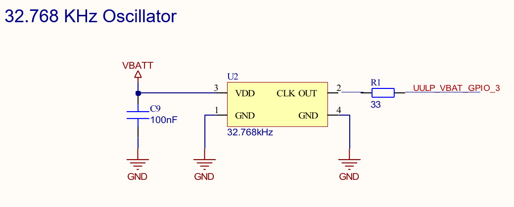
LF Clock Option
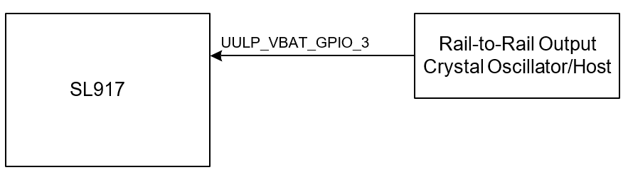
Note: For WiFi, BLE, and Co-Ex power saving use cases, Ezurio mandates an external clock to be used on UULP_VBAT_GPIO_3 pin for the low-frequency clock source to maintain timing accuracy requirements and optimize power consumption.
Flash Memory Configurations
Host Interface
Notes:
- In UART mode, ensure that the input signals, UART_RX and UART_CTS are not floating when the device is powered up and reset is de-asserted. This can be done by ensuring that the host processor configures its signals (outputs) before de-asserting the reset.
In HSPI mode, ensure that the input signals, HSPI_CSN and HSPI_CLK are not floating when the device is powered up and reset is de-asserted. This can be done by ensuring that the external Host processor configures its signals (outputs) before de-asserting the reset. HSPI_INTR is the interrupt signal driven by the secondary device. This signal may be configured as Active-high or Active-low. If it is active-high, an external pull-down resistor is required. If it is active-low, an external pull-up resistor is required. The following actions can be carried out by the host processor during power-up of the device, and before/after ULP Sleep mode.
- To use the signal in the Active-high or Active-low mode, ensure that during the power up of the device, the Interrupt is disabled in the Host processor before de-asserting the reset. After de-asserting the reset, the Interrupt needs to be enabled only after the HSPI initialization is done and the Interrupt mode is programmed to either Active-high or Active-low mode as required.
- The Host processor needs to disable the interrupt before the ULP Sleep mode is entered and enable it after HSPI interface is reinitialized upon wakeup from ULP Sleep.
- In SDIO mode, pull-up resistors should be present on SDIO_CMD & SDIO Data lines as per the SDIO physical layer specification version 2.0.
- 33ohm on SDIO_CLK/HSPI_CLK has to be near the source of the clock, and not near the module.
- R5 to R11 are optional resistors for Signal Integrity.
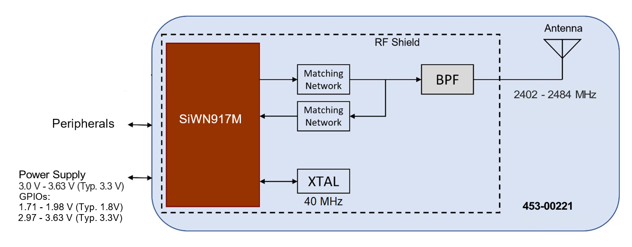
SL917 NCP Schematics for parts with Integral Antenna
System Supplies
Notes:
- Place all the decoupling capacitors close to the module pins.
- IO_VDD, SDIO_IO_VDD, ULP_IO_VDD can be powered independently by different voltage sources based on their corresponding signals voltage levels requirements. Voltages must be as per Table 7.2 Recommended Operating Conditions on page 26.
- Even if GPIOs are not used, their respective IO domains must still be connected to the power supply.
RF, Debug, and Reset Connection
Note:
- It is mandatory to follow the reference schematics for optimal RF performance.
GPIO Connection
Notes:
- Place all the decoupling capacitors close to the module pins.
- IO_VDD, SDIO_IO_VDD, ULP_IO_VDD can be powered independently by different voltage sources based on their corresponding signals voltage levels requirements. Voltages must be as per Table 7.2 Recommended Operating Conditions on page 26.
- Even if GPIOs are not used, their respective IO domains must still be connected to the power supply.
- R5 through R10 are optional resistors for signal integrity.
- R5 33ohm on SDIO_CLK/HSPI_CLK has to be near the source of the clock.
RESET
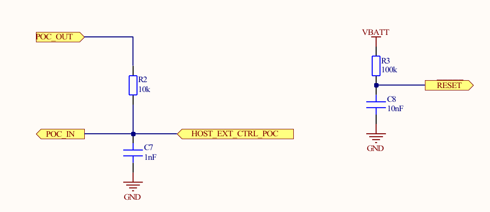
Notes:
- The configuration shown allows for blackout monitor functionality along with external reset of the embedded SiWN917M IC.
- The POC_IN signal connects to the POC_IN pin on the SiWN917M. POC_IN resets all the internal blocks of the IC.
- The Si917_RESET signal connects to the RESET_N pin on the SiWN917M. It is recommended to use the RC filter as shown. RE- SET_N is an open-drain output pin that will be pulled low when POC_IN goes low.
- The POC_OUT signal connects to the POC_OUT pin on the SiWN917M. POC_OUT is an active-low, push-pull output from the internal blackout monitor. In this configuration, it is isolated from the external HOST_EXT_CTRL_POC signal with a series resistor. In applications without external host control (HOST_EXT_CTRL_POC), POC_OUT may be directly connected to POC_IN. Without external host control to the POC_IN pin, the IC cannot be reset multiple times after power-on.
- The HOST_EXT_CTRL_POC signal connects to a GPIO of an external host processor. In this configuration, HOST_EXT_CTRL_POC must be an open-drain output to allow POC_OUT to control POC_IN.
- HOST_EXT_CTRL_POC must be at the same voltage level as the VBATT supply pin.
LF Clock Option
Note: For WiFi, BLE, and Co-Ex power saving use cases, Ezurio mandates an external clock to be used on UULP_VBAT_GPIO_3 pin for the low-frequency clock source to maintain timing accuracy requirements and optimize power consumption.
Flash Memory Configurations
Host Interface
Notes:
- In UART mode, ensure that the input signals, UART_RX and UART_CTS are not floating when the device is powered up and reset is de-asserted. This can be done by ensuring that the host processor configures its signals (outputs) before de-asserting the reset.
In HSPI mode, ensure that the input signals, HSPI_CSN and HSPI_CLK are not floating when the device is powered up and reset is de-asserted. This can be done by ensuring that the external Host processor configures its signals (outputs) before de-asserting the reset. HSPI_INTR is the interrupt signal driven by the secondary device. This signal may be configured as Active-high or Active-low. If it is active-high, an external pull-down resistor is required. If it is active-low, an external pull-up resistor is required. The following actions can be carried out by the host processor during power-up of the device, and before/after ULP Sleep mode.
- To use the signal in the Active-high or Active-low mode, ensure that during the power up of the device, the Interrupt is disabled in the Host processor before de-asserting the reset. After de-asserting the reset, the Interrupt needs to be enabled only after the HSPI initialization is done and the Interrupt mode is programmed to either Active-high or Active-low mode as required.
- The Host processor needs to disable the interrupt before the ULP Sleep mode is entered and enable it after HSPI interface is reinitialized upon wakeup from ULP Sleep.
- In SDIO mode, pull-up resistors should be present on SDIO_CMD & SDIO Data lines as per the SDIO physical layer specification version 2.0.
- 33ohm on SDIO_CLK has to be near the source of the clock, and not near the module.
- R5 to R11 are optional resistors for Signal Integrity.
Bill of Materials
BOM for Parts with RF Pin
| Line No | Quantity | Designator | Value | Description | Manufacturer | Manufacturer PN | Tolerance | Rating |
|---|---|---|---|---|---|---|---|---|
| 1 | 5 | C1, C3, C4, C5, C6 | 1uF | CAP CER 0402 X5R 1uF 10V 10% | - | - | 10% | 10 V |
| 2 | 1 | C2 | 18pF | CAP CER 0201 C0G 18pF 25V 2% | - | - | 2% | 25V |
| 3 | 1 | C7 | 1nF | CAP CER 0402 X7R 1nF 16V 10% | - | - | 10% | 16V |
| 4 | 1 | C8 | 10nF | CAP CER 0402 X7R 10nF 16V 10% | - | - | 10% | 16V |
| 5 | 1 | C9 | 100nF | CAP CER 0402 X7R 100nF 50V 10% | - | - | 10% | 50V |
| 6 | 1 | J1 | U.FL-R- SMT-1 | CONN RF 500HM UFL_2.6x2.6 SMD | - | - | ||
| 7 | 1 | L1 | 6.2 nH | IND Fixed 0201 6.2nH 300mA 600mOhm 3% | - | - | 3% | 300mA |
| 8 | 8 | R1, R5, R6, R7, R8, R9, R10, R11 | 33 | RES 0402 33R 1/16W 1% 100ppm | - | - | 1% | 62.5 mW |
| 9 | 1 | R2 | 10k | RES 0402 10K 1/16W 5% 200ppm | - | - | 5% | 63mW |
| 10 | 1 | R3 | 100k | RES 0402 100K 1/16W 1% 100ppm | - | - | 1% | 63mW |
| 11 | 1 | U2 | 32.768 kHz | SiTIME CRYSTAL CSPBGA 32.768kHz 10pF 100ppm | SiTIME | SiT1532A I-J4- DCC-32.7 68 | ||
| 12 | 1 | U1 | 453-00219 | SL917 Module based on SiW917Y1GN | Ezurio |
BOM for parts with Integral Antenna
| Line No | Quantity | Designator | Value | Description | Manufacturer | Manufacturer PN | Tolerance | Rating |
|---|---|---|---|---|---|---|---|---|
| 1 | 5 | C1, C3, C4, C5, C6 | 1uF | CAP CER 0402 X5R 1uF 10V 10% | - | - | 10% | 10 V |
| 2 | 1 | C2 | 18pF | CAP CER 0201 C0G 18pF 25V 2% | - | - | 2% | 25V |
| 3 | 1 | C7 | 1nF | CAP CER 0402 X7R 1nF 16V 10% | - | - | 10% | 16V |
| 4 | 1 | C8 | 10nF | CAP CER 0402 X7R 10nF 16V 10% | - | - | 10% | 16V |
| 5 | 1 | C9 | 100nF | CAP CER 0402 X7R 100nF 50V 10% | - | - | 10% | 50V |
| 6 | 1 | J1 | U.FL-R- SMT-1 | CONN RF 500HM UFL_2.6x2.6 SMD | - | - | ||
| 7 | 1 | L1 | 6.2 nH | IND Fixed 0201 6.2nH 300mA 600mOhm 3% | - | - | 3% | 300mA |
| 8 | 8 | R1, R5, R6, R7, R8, R9, R10, R11 | 33 | RES 0402 33R 1/16W 1% 100ppm | - | - | 1% | 62.5 mW |
| 9 | 1 | R2 | 10k | RES 0402 10K 1/16W 5% 200ppm | - | - | 5% | 63mW |
| 10 | 1 | R3 | 100k | RES 0402 100K 1/16W 1% 100ppm | - | - | 1% | 63mW |
| 11 | 1 | U2 | 32.768 kHz | SiTIME CRYSTAL CSPBGA 32.768kHz 10pF 100ppm | SiTIME | SiT1532A I-J4- DCC-32.7 68 | ||
| 12 | 1 | U1 | 453-00221 | SL917 Module based on SiW917Y1GA | Ezurio |
Electrical Characteristics
Absolute Maximum Ratings
Stresses beyond those listed below may cause permanent damage to the device. This is a stress rating only and functional operation of the devices at those or any other conditions beyond those indicated in the operation listings of this specification is not implied. Exposure to maximum rating conditions for extended periods may affect device reliability. For more information on the available quality and reliability data, see the Quality and Reliability Monitor Report at https://www.silabs.com/about-us/quality
Note: All the specifications are preliminary and subject to change.
| Parameter | Symbol | Test Conditon | Min | Typ | Max | Unit |
|---|---|---|---|---|---|---|
| Storage temperature | Tstore | -40 | — | 125 | oC | |
| Maximum junction temperature | Tj(max) | — | 125 | oC | ||
| 3.3V power supply for the on-chip Buck, RF circuit, and UULP IOs | VBATT | -0.5 | — | 3.63 | V | |
| I/O supply for GPIOs | IO_VDD | -0.5 | — | 3.63 | V | |
| I/O supply for SDIO I/Os | SDIO_IO_VDD | -0.5 | — | 3.63 | V | |
| I/O supply for QSPI flash signals | FLASH_IO_VDD | -0.5 | — | 3.63 | V | |
| I/O supply for ULP I/Os | ULP_IO_VDD | -0.5 | — | 3.63 | V | |
| DC voltage on any I/O pin 1 | VIO_PIN | -0.5 | — | VDD + 0.5 | V | |
| Total average max current into chip | Ipmax | — | — | 500 | mA | |
| Current per I/O pin | IIOMAX | Sink | — | — | 100 | mA |
| Source | — | — | 100 | mA |
Note:
- VDD = I/O supply domain pin. Refer to pin description tables for supply domain associated with each I/O.
Recommended Operating Conditions
Note: The device may operate continuously at the maximum allowable ambient Tambient rating as long as the maximum junction Tjunction(max) is not exceeded. For an application with significant power dissipation, the allowable Tambient may be lower than the maximum Tambient rating. Tambient = Tjunction(max) - (ΘJA x Power Dissipation). Refer to the Thermal Characteristics table for ΘJA.
| Parameter | Symbol | Test Condition | Min. | Typ. | Max. | Units |
|---|---|---|---|---|---|---|
| Ambient temperature | Tambient | -40 | 25 | 85 | oC | |
| Junction temperature | Tjunction | 105 | oC | |||
| 3.3V power supply for the on- chip Buck, RF Power Amplifier, UULP I/Os | VBATT | 3.0 | 3.3 | 3.63 | V | |
| I/O supply for Flash | FLASH_IO_VD D | 1.71 | 1.8 | 1.98 | V | |
I/O supply for GPIOs |
IO_VDD1 | 1.8 V nominal operation | 1.71 | 1.8 | 1.98 |
V |
| 3.3 V nominal operation | 2.97 | 3.3 | 3.63 | |||
I/O supply for SDIO I/Os |
SDIO_IO_VDD1 | 1.8 V nominal operation | 1.71 | 1.8 | 1.98 |
V |
| 3.3 V nominal operation | 2.97 | 3.3 | 3.63 | |||
| I/O supply for ULP I/Os | ULP_IO_VDD1 | 1.8 V nominal operation | 1.71 | 1.8 | 1.98 |
V |
| 3.3 V nominal operation | 2.97 | 3.3 | 3.63 |
Note:
- Supplies can operate at a nominal 3.3 V or 1.8 V level independent of the other supplies in the system.
DC Electrical Characteristics
RESET_N Pin
| Parameter | Symbol | Test Condition | Min | Typ | Max | Unit |
|---|---|---|---|---|---|---|
| High level input voltage | VIH | RESET_N pin, VBATT = 3.3 V | 0.8 * VBATT | — | — | V |
| Low level input voltage | VIL | RESET_N pin, VBATT = 3.3 V | — | — | 0.3 * VBATT | V |
Power On Control (POC) and Reset
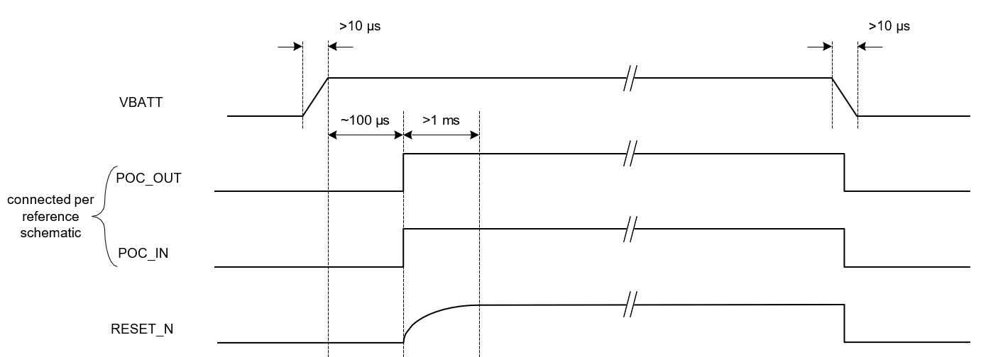
There are three signals involved in power-on control and reset of the device:
- POC_IN: When pulled low, POC_IN will reset all of the internal blocks in the device. The POC_IN signal can be controlled either by external circuitry, by POC_OUT, or both.
- RESET_N: RESET_N is an open-drain signal which will be pulled low during a chip reset. It is released after POC_IN is high. RESET_N should be connected to an RC circuit to fulfill the timing requirements shown in Power Up Sequence.
- POC_OUT: The POC_OUT signal is the output of the internal blackout supply monitor. POC_OUT is distributed to all I/O cells to prevent the I/O cells from powering up in an undesired configuration and is also used inside the IC to place the IC in a safe state until a valid supply is available for proper operation. During power up, POC_OUT stays low until the VBATT reaches 1.6 V. After the VBATT supply exceeds 1.6 V, POC_OUT becomes high and normal operation begins. If VBATT becomes lower than the blackout threshold voltage, POC_OUT will return low. POC_OUT can be used to provide chip reset by connecting to POC_IN in a loopback configuration.
The recommended schematic for the reset signals is shown in Reset.
Power Up Sequence shows the signal timing when POC_OUT, POC_IN, and RESET_N are connected per the recommended schematic. The POC_IN-to-RESET_N delay will occur when POC_IN transitions from low to high.
In this configuration the system only has to control the supply (VBATT) during power-up and power down and need not control POC_IN externally. On power-up the chip will be reset internally. The power-down sequence will follow VBATT and external control of POC_IN is not required.
Power Up Sequence
If the chip is to be reset from an external host device while powered up, the POC_IN signal should be pulled low for at least 10 ms as shown below. Upon release of POC_IN, the POC_IN-to-RESET_N delay will occur.
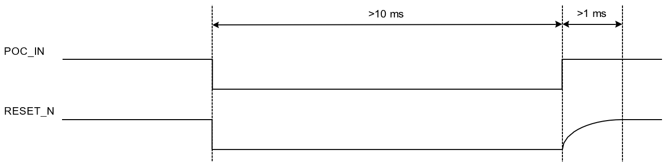
In the above timing diagrams, it is assumed that all supplies including VBATT are connected together. If they are not connected together and independently controlled, then the guidance below must be followed.
Case 1: POC is looped back and there is no external control for POC_IN
- All supplies can be enabled at the same time, if possible
- If supplies cannot be enabled at the same time, the VBATT supplies should be powered up first and all other supplies should be powered on at least 1 ms before RESET_N is high. The RC circuit controlling RESET_N must be adjusted to provide the appropriate delay.
- While powering down, supplies can be powered off simultaneously, or with VBATT the last to be disabled.
Case 2: POC is looped back and there is external control for POC_IN during power-up / power-down.
- All supplies can be enabled at the same time, or VBATT may be enabled before other supplies.
- POC_IN should be kept low for at least 600 us after all the supplies have settled.
- On power-down, POC_IN can be driven low before disabling the supplies. Supplies can be powered off simultaneously, or with VBATT the last to be disabled.
Signal Levels and Interface Specs
Digital I/O Signals
| Parameter | Symbol | Test Condition | Min | Typ | Max | Unit |
|---|---|---|---|---|---|---|
| High level input voltage | VIH | IO_VDDx = 3.3 V | 2 | — | — | V |
| IO_VDDx = 1.8 V | 1.17 | — | — | V | ||
| Low level input voltage | VIL | IO_VDDx = 3.3 V | — | — | 0.8 | V |
| IO_VDDx = 1.8 V | — | — | 0.63 | V | ||
| Low level output voltage | VOL | — | — | 0.4 | V | |
| High level output voltage | VOH | IO_VDDx - 0.4 | — | — | V | |
| Low level output current | IOL | GPIO_* and ULP_GPIO_* pins | 2 | 4 | 12 | mA |
| UULP_GPIO_* | 1 | — | 2 | mA | ||
| High level output current | IOH | GPIO_* and ULP_GPIO_* pins | 2 | 4 | 12 | mA |
| UULP_GPIO_* | 1 | — | 2 | mA |
Flash LDO Electrical Specifications - Regulation Mode
| Parameter | Symbol | Test Condition | Min | Typ | Max | Unit |
|---|---|---|---|---|---|---|
| Input Supply Voltage (VBATT) | Vin | Flash LDO in Regulation Mode | 2.97 | 3.3 | 3.63 | V |
| Output Voltage Range (VBATT) | Vout | — | 1.8 | — | V | |
| Load current | Iload | — | — | 48 | mA | |
| Line Regulation | REGline | Vin Changed from 2.97 V to 3.63 V | — | — | 0.6 | % |
| Load Regulation | REGload | Iload changed from 0 mA to 48 mA | — | — | 1.4 | % |
AC Characteristics
Clock Specifications
The SL917 NCP module includes the following clock options:
- Low frequency clock options for sleep manager and RTC
- Internal 32 kHz RC oscillator (for applications with low timing accuracy requirements only, typical accuracy is +/- 1.2%)
- 32.768 kHz LVCMOS rail-to-rail external oscillator input pin UULP_VBAT_GPIO_3 for external oscillator or host clock
- High frequency 40 MHz clock for NWP, Cortex-M4, baseband subsystem and the radio
- 40 MHz clock is integrated inside the module, and no external clock needs to be provided
The chipsets have integrated internal oscillators including crystal oscillators to generate the required clocks. Integrated crystal oscillators enable the use of low-cost passive crystal components. Additionally, in a system where an external clock source is already present, the clock can be reused. The following are the recommended options for the clocks for different functionalities:
32 kHz External Sources:
Note: For W-iFi, BLE, and Co-Ex power saving use cases, Ezurio mandates an external clock to be used on UULP_VBAT_GPIO_3 pin for the low-frequency clock source to maintain timing accuracy requirements and optimize power consumption.
Option 1: From Host MCU/MPU LVCMOS rail to rail clock input on UULP_VBAT_GPIO_3
Option 2: External clock oscillator providing LVCMOS rail to rail clock input on UULP_VBAT_GPIO_3 (Nano-drive clock should not be supplied).
Low Frequency Clock
Low-frequency clock selection can be done through software. The RC oscillator clock is not suited for high timing accuracy applications and may increase overall system current consumption in duty-cycled power modes.
32 kHZ Internal RC Oscillator
| Parameter | Symbol | Test Condition | Min | Typ | Max | Unit |
|---|---|---|---|---|---|---|
| Oscillator Frequency | Fosc | 32.0 | kHz | |||
| Frequency Variation with Temp and Voltage | Fosc_Acc | 1.2 | % |
32.768 kHz External Oscillator
An external 32.768 kHz low-frequency clock can be fed through UULP_VBAT_GPIO_3.
Rail to Rail Table - 32.768 kHz External
| Parameter | Symbol | Test Condition | Min | Typ | Max | Unit |
|---|---|---|---|---|---|---|
| Oscillator Frequency | fosc | — | 32.768 | — | kHz | |
| Frequency Variation with Temp and Voltage | fosc_Acc | -100 | — | 100 | ppm | |
| Input duty cycle | DCin | 30 | 50 | 70 | % | |
| Input AC peak-peak voltage swing at input pin. | VAC | -0.3 | — | VBATT +/- 10% | Vpp |
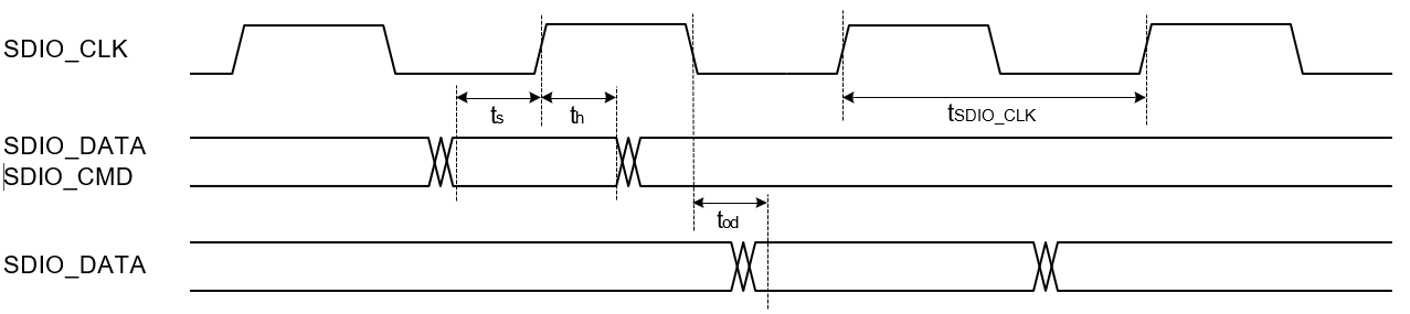
SDIO 2.0 Secondary
Full Speed Mode
| Parameter | Symbol | Test Condition | Min | Typ | Max | Unit |
|---|---|---|---|---|---|---|
| SDIO_CLK | fsdio_clk | — | — | 25 | MHz | |
| SDIO_DATA, SDIO_CMD input setup time | ts | 4 | — | — | ns | |
| SDIO_DATA, SDIO_CMD in- put hold time | th | 1.2 | — | — | ns | |
| SDIO_DATA, clock to output delay | tod | — | — | 13 | ns | |
| Output Load | CL | 5 | — | 10 | pF |
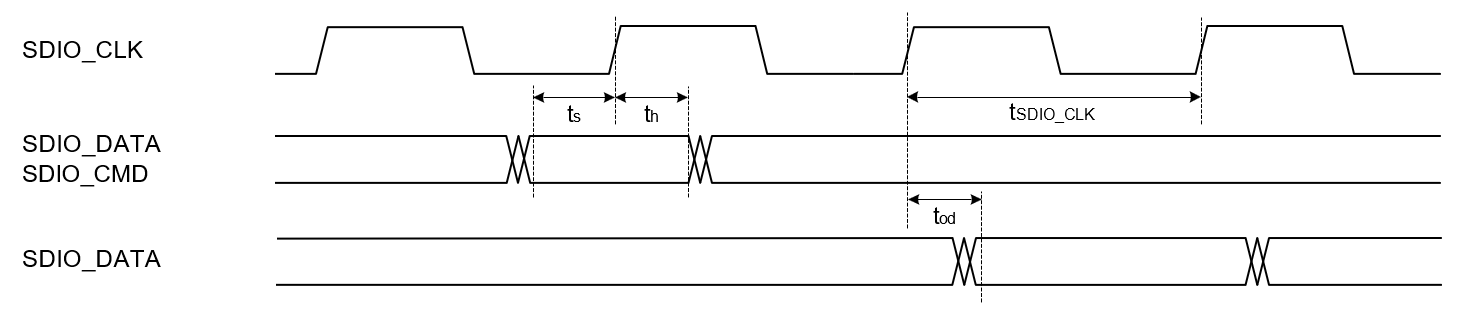
High Speed Mode
| Parameter | Symbol | Test Condition | Min | Typ | Max | Unit |
|---|---|---|---|---|---|---|
| SDIO_CLK | fsdio_clk | 25 | — | 50 | MHz | |
| SDIO_DATA, input setup time | ts | 4 | — | — | ns | |
| SDIO_DATA, input hold time | th | 1.2 | — | — | ns | |
| SDIO_DATA, clock to output delay | tod | 2.5 | — | 13 | ns | |
| Output Load | CL | 5 | — | 10 | pF |
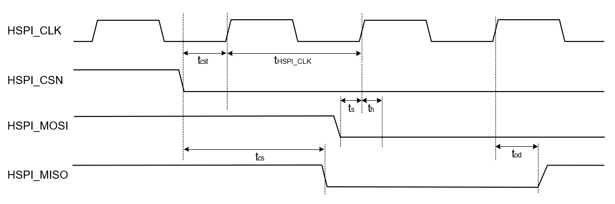
HSPI Secondary
Low Speed Mode
| Parameter | Symbol | Test Condition | Min | Typ | Max | Unit |
|---|---|---|---|---|---|---|
| HSPI_CLK | fhspi | 0 | — | 25 | MHz | |
| HSPI_CSN to output delay | tcs | — | — | 7.5 | ns | |
| HSPI_CSN to input setup time | tcst | 4.5 | — | — | ns | |
| HSPI_MOSI, input setup time | ts | 1.4 | — | — | ns | |
| HSPI_MOSI, input hold time | th | 1.5 | — | — | ns | |
| HSPI_MISO, clock to output delay | tod | — | — | 8.75 | ns | |
| Output Load | CL | 5 | — | 10 | pF |
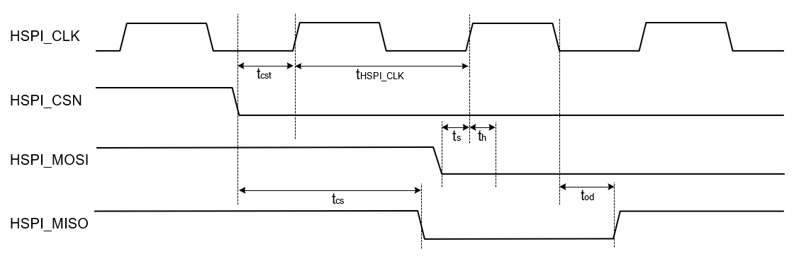
In low speed mode, HSPI_MISO data is driven on the falling edge of HSPI_CLK, and HSPI_MOSI is read on the rising edge of HSPI_CLK.
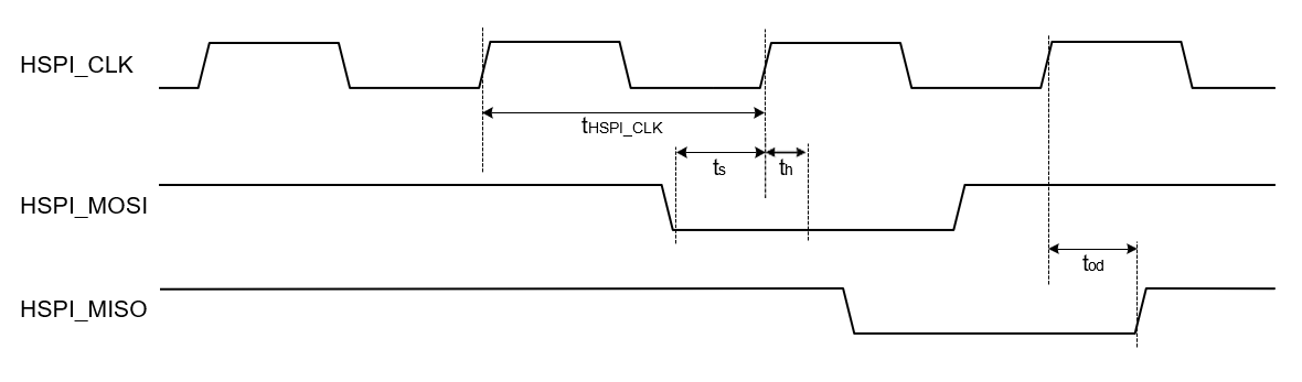
High Speed Mode
| Parameter | Symbol | Test Condition | Min | Typ | Max | Unit |
|---|---|---|---|---|---|---|
| HSPI_CLK | fhspi | 25 | — | 80 | MHz | |
| HSPI_CSN to output delay | tcs | — | — | 7.5 | ns | |
| HSPI_CSN to input setup time | tcst | 4.5 | — | — | ns | |
| HSPI_MOSI, input setup time | ts | 1.4 | — | — | ns | |
| HSPI_MOSI, input hold time | th | 1.4 | — | — | ns | |
| HSPI_MISO, clock to output delay | tod | 1.5 | — | 8.75 | ns | |
| Output Load | CL | 5 | — | 10 | pF |
In high speed mode, HSPI_MISO data is driven on the rising edge of HSPI_CLK, and HSPI_MOSI is read on the rising edge of HSPI_CLK.
Ultra High Speed Mode
| Parameter | Symbol | Test Condition | Min | Typ | Max | Unit |
|---|---|---|---|---|---|---|
| HSPI_CLK | fhspi | 80 | — | 100 | MHz | |
| HSPI_MOSI, input setup time | ts | 1.4 | — | — | ns | |
| HSPI_MOSI, input hold time | th | 1.4 | — | — | ns | |
| HSPI_MISO, clock to output delay | tod | 1.5 | — | 8.75 | ns | |
| Output Load | CL | 5 | — | 10 | pF |
Note:
- In ultra high-speed modes, the data on HSPI_MISO is driven on the rising edge of the SPI_CLK. The data on SPI_MOSI is read on the rising edge of the SPI_CLK.
In ultra high speed mode, HSPI_MISO data is driven on the rising edge of HSPI_CLK, and HSPI_MOSI is read on the rising edge of HSPI_CLK.
GPIO
| Parameter | Symbol | Test Condition | Min | Typ | Max | Unit |
|---|---|---|---|---|---|---|
| Rise time | trf | Pin configured as output | 1 | — | 5 | ns |
| Fall time | tff | Pin configured as output | 0.9 | — | 5 | ns |
| Rise time | tr | Pin configured as input | 0.3 | — | 1.3 | ns |
| Fall time | tf | Pin configured as input | 0.2 | — | 1.2 | ns |
In-Package Flash Memory
| Parameter | Symbol | Test Condition | Min | Typ | Max | Unit |
|---|---|---|---|---|---|---|
| Endurance | Nendu | Sector erase/program | 10000 | — | — | cycles |
| Page erase/program, page in large sector | 10000 | — | — | cycles | ||
| Page erase/program, page in small sector | 10000 | — | — | cycles | ||
| Retention time | tret | Powered | 10 | — | — | years |
| Unpowered | 10 | — | — | years | ||
| Block Erase time (32 KB) | ter | Page, sector or multiple consecutive sectors | — | 150 | 1400 | ms |
| Page programming time | tprog | — | 0.5 | 3 | ms | |
| Chip Erase time | tce | — | 20 | 65 | s |
Radio Characteristics
In the sub-sections below,
- All numbers are measured at TA = 25°C, VBATT = 3.3 V
- Please refer to Schematics. The integrated RF front end includes the matching network, RF switch, and a band-pass filter.
Supported WLAN channels for different regions include:
- US: Channels 1 (2412 MHz) through 11 (2462 MHz)
- Europe: Channels 1 (2412 MHz) through 13 (2472 MHz)
- Japan: Channels 1 (2412 MHz) through 14 (2484 MHz), Channel 14 supports 1 and 2 Mbps data rates only
WLAN 2.4 GHz Radio Receiver Characteristics
Receiver Characteristics on High-Performance (HP) Mode
Unless otherwise indicated, typical conditions are: TA = 25 °C. VBATT = 3.3 V. Remaining supplies are at typical operating conditions. Parameters are referred at antenna port.
| Parameter | Symbol | Test Condition | Min | Typ | Max | Unit |
|---|---|---|---|---|---|---|
| Sensitivity for 20 MHz Bandwidth 1, 2 | SENS | 802.11b 1 Mbps DSSS 3 | — | -95 | — | dBm |
| 802.11b 11 Mbps CCK 3 | — | -86 | — | dBm | ||
| 802.11g 6 Mbps OFDM 4 | — | -90.5 | — | dBm | ||
| 802.11g 54 Mbps OFDM 4 | — | -74 | — | dBm | ||
| 802.11n HT20 MCS0 Mixed Mode5 | — | -89.5 | — | dBm | ||
| 802.11n HT20 MCS7 Mixed Mode 5 | — | -69.5 | — | dBm | ||
| 802.11ax HE20 MCS0 SU 6 | — | -89 | — | dBm | ||
| 802.11ax HE20 MCS7 SU 6 | — | -68.5 | — | dBm | ||
| 802.11ax HE20 MCS0 ER 6 | — | -91 | — | dBm | ||
| Maximum Input Level for PER below 10% | RXSAT | 802.11b | — | 5 | — | dBm |
| 802.11g | — | 0 | — | dBm | ||
| 802.11n | — | 0 | — | dBm | ||
| 802.11ax | — | 0 | — | dBm | ||
| RSSI Accuracy Range | RSSIRNG | — | +4/-5 | — | dB | |
| Adjacent Channel Interfer- ence 7 | ACI | 802.11b 1 Mbps DSSS 3 8 | — | 51 | — | dB |
| 802.11b 11 Mbps CCK 3 8 | — | 34 | — | dB | ||
| 802.11g 6 Mbps OFDM 4 9 | — | 43 | — | dB | ||
| 802.11g 54 Mbps OFDM 4 9 | — | 26 | — | dB | ||
| 802.11n HT20 MCS0 Mixed Mode 59 | — | 33 | — | dB | ||
| 802.11n HT20 MCS7 Mixed Mode 59 | — | 12 | — | dB | ||
| 802.11ax HE20 MCS0 SU6 9 | — | 21 | — | dB | ||
| 802.11ax HE20 MCS7 SU6 9 | — | 6 | — | dB | ||
| Alternate Adjacent Channel Interference 7 | AACI | 802.11b 1 Mbps DSSS 3 8 | — | 54 | — | dB |
| 802.11b 11 Mbps CCK 3 8 | — | 37 | — | dB | ||
| 802.11g 6 Mbps OFDM 4 9 | — | 54 | — | dB | ||
| 802.11g 54 Mbps OFDM 4 9 | — | 34 | — | dB | ||
| 802.11n HT20 MCS0 Mixed Mode 59 | — | 53 | — | dB | ||
| 802.11n HT20 MCS7 Mixed Mode 59 | — | 33 | — | dB | ||
| 802.11ax HE20 MCS0 SU6 9 | — | 53 | — | dB | ||
| 802.11ax HE20 MCS7 SU 6 9 | — | 33 | — | dB |
Notes:
- RX Sensitivity Variation is up to 3 dB for channels (1, 2, 3, 4, 5, 9, and 10) at typical / room temperature.
- RX Sensitivity may be degraded up to 4 dB for channels (6, 7, 8, 11, 12, 13 and 14) at typical / room temperature.
- 802.11b, Packet size is 1024 bytes, < 8% PER limit, Carrier modulation is non-DCM
- 802.11g, Packet size is 1024 bytes, < 10% PER limit, Carrier modulation is non-DCM
- 802.11n, Packet size is 4096 bytes, < 10% PER limit, Carrier modulation is non-DCM
- 802.11ax, Packet size is 4096 bytes, < 10% PER limit, Carrier modulation is non-DCM
- ACI / AACI is calculated as Interferer Power(dBm)- Inband power(dBm)
- Desired signal power is 6 dB above standard defined sensitivity level
- Desired signal power is 3 dB above standard defined sensitivity level
Receiver Characteristics on Low-Power (LP) Mode
Unless otherwise indicated, typical conditions are: TA = 25 °C. VBATT = 3.3 V. Remaining supplies are at typical operating conditions. Parameters are referred at antenna port.
| Parameter | Symbol | Test Condition | Min | Typ | Max | Unit |
| Sensitivity for 20 MHz Band- width1 2 | SENS | 802.11b 1 Mbps DSSS 3 | — | -95 | — | dBm |
| 802.11b 11 Mbps CCK 3 | — | -86 | — | dBm | ||
| 802.11g 6 Mbps OFDM 4 | — | -90 | — | dBm | ||
| 802.11g 36 Mbps OFDM 4 | — | -79 | — | dBm | ||
| 802.11n HT20 MCS0 Mixed Mode 5 | — | -88 | — | dBm | ||
| 802.11n HT20 MCS4 Mixed Mode 5 | — | -77 | — | dBm | ||
| Maximum Input Level for PER below 10% | RXSAT | 802.11b | — | -2.5 | — | dBm |
| 802.11g | — | 1.5 | — | dBm | ||
| 802.11n | — | 0.5 | — | dBm | ||
| RSSI Accuracy Range | RSSIRNG | — | +4/-6 | — | dB | |
| Adjacent Channel Interference6 | ACI | 802.11b 1 Mbps DSSS 3 7 | — | 52 | — | dB |
| 802.11b 11 Mbps CCK 3 7 | — | 33 | — | dB | ||
| 802.11g 6 Mbps OFDM 4 8 | — | 44 | — | dB | ||
| 802.11g 36 Mbps OFDM 4 8 | — | 29 | — | dB | ||
| 802.11n HT20 MCS0 Mixed Mode 58 | — | 33 | — | dB | ||
| 802.11n HT20 MCS4 Mixed Mode 58 | — | 20 | — | dB | ||
| Alternate Adjacent Channel Interference6 | AACI | 802.11b 1 Mbps DSSS3 7 | — | 53 | — | dB |
| 802.11b 11 Mbps CCK 3 7 | — | 37 | — | dB | ||
| 802.11g 6 Mbps OFDM 4 8 | — | 53 | — | dB | ||
| 802.11g 36 Mbps OFDM 4 8 | — | 37 | — | dB | ||
| 802.11n HT20 MCS0 Mixed Mode 58 | — | 52 | — | dB | ||
| 802.11n HT20 MCS4 Mixed Mode 58 | — | 36 | — | dB |
Notes:
- RX Sensitivity Variation is up to 3 dB for channels (1, 2, 3, 4, 5, 9, and 10) at typical / room temperature
- RX Sensitivity may be degraded up to 4 dB for channels (6, 7, 8, 11, 12, 13 and 14) at typical / room temperature
- 802.11b, Packet size is 1024 bytes, < 8% PER limit, Carrier modulation is non-DCM
- 802.11g, Packet size is 1024 bytes, < 10% PER limit, Carrier modulation is non-DCM
- 802.11n, Packet size is 4096 bytes, < 10% PER limit, Carrier modulation is non-DCM
- ACI / AACI is calculated as Interferer Power(dBm)- Inband power(dBm)
- Desired signal power is 6 dB above standard defined sensitivity level
- Desired signal power is 3 dB above standard defined sensitivity level
Receiver Characteristics on Low-Power (LP) Mode
Unless otherwise indicated, typical conditions are: TA = 25 °C. VBATT = 3.3 V. Remaining supplies are at typical operating conditions. Parameters are referred at antenna port.
| Parameter | Symbol | Test Condition | Min | Typ | Max | Unit |
|---|---|---|---|---|---|---|
| Sensitivity for 20 MHz Band- width 1 2 | SENS | 802.11b 1 Mbps DSSS 3 | — | -95 | — | dBm |
| 802.11b 11 Mbps CCK 3 | — | -86 | — | dBm | ||
| 802.11g 6 Mbps OFDM 4 | — | -90 | — | dBm | ||
| 802.11g 36 Mbps OFDM 4 | — | -79 | — | dBm | ||
| 802.11n HT20 MCS0 Mixed Mode 5 | — | -88 | — | dBm | ||
| 802.11n HT20 MCS4 Mixed Mode 5 | — | -77 | — | dBm | ||
| Maximum Input Level for PER below 10% | RXSAT | 802.11b | — | -2.5 | — | dBm |
| 802.11g | — | 1.5 | — | dBm | ||
| 802.11n | — | 0.5 | — | dBm | ||
| RSSI Accuracy Range | RSSIRNG | — | +4/-6 | — | dB | |
| Adjacent Channel Interference6 | ACI | 802.11b 1 Mbps DSSS 3 7 | — | 52 | — | dB |
| 802.11b 11 Mbps CCK 3 7 | — | 33 | — | dB | ||
| 802.11g 6 Mbps OFDM 4 8 | — | 44 | — | dB | ||
| 802.11g 36 Mbps OFDM 4 8 | — | 29 | — | dB | ||
| 802.11n HT20 MCS0 Mixed Mode 58 | — | 33 | — | dB | ||
| 802.11n HT20 MCS4 Mixed Mode 58 | — | 20 | — | dB | ||
| Alternate Adjacent Channel Interference6 | AACI | 802.11b 1 Mbps DSSS 3 7 | — | 53 | — | dB |
| 802.11b 11 Mbps CCK 3 7 | — | 37 | — | dB | ||
| 802.11g 6 Mbps OFDM 4 8 | — | 53 | — | dB | ||
| 802.11g 36 Mbps OFDM 4 8 | — | 37 | — | dB | ||
| 802.11n HT20 MCS0 Mixed Mode 58 | — | 52 | — | dB | ||
| 802.11n HT20 MCS4 Mixed Mode 58 | — | 36 | — | dB |
Notes:
- RX Sensitivity Variation is up to 3 dB for channels (1, 2, 3, 4, 5, 9, and 10) at typical / room temperature
- RX Sensitivity may be degraded up to 4 dB for channels (6, 7, 8, 11, 12, 13 and 14) at typical / room temperature
- 802.11b, Packet size is 1024 bytes, < 8% PER limit, Carrier modulation is non-DCM
- 802.11g, Packet size is 1024 bytes, < 10% PER limit, Carrier modulation is non-DCM
- 802.11n, Packet size is 4096 bytes, < 10% PER limit, Carrier modulation is non-DCM
- ACI / AACI is calculated as Interferer Power(dBm)- Inband power(dBm)
- Desired signal power is 6 dB above standard defined sensitivity level
- Desired signal power is 3 dB above standard defined sensitivity level
WLAN 2.4 GHz Transmitter Characteristics
Transmitter Characteristics with 3.3V Supply
Unless otherwise indicated, typical conditions are: TA = 25°C, VBATT = 3.3V. Remaining supplies are at typical operating conditions. Parameters are referred at antenna port.
| Parameter | Symbol | Test Condition | Min | Typ | Max | Unit |
|---|---|---|---|---|---|---|
| Transmit Power for 20 MHz Bandwidth, with EVM limits 1, 2,5 | POUT | 802.11b 1 Mbps DSSS, EVM< -9 dB | — | 17 | — | dBm |
| 802.11b 11 Mbps CCK, EVM< -9 dB | — | 17 | — | dBm | ||
| 802.11g 6 Mbps OFDM, EVM< -5 dB 3 | — | 17.5 | — | dBm | ||
| 802.11g 54 Mbps OFDM, EVM< -25 dB 3 | — | 13.5 | — | dBm | ||
| 802.11n HT20 MCS0 Mixed Mode, EVM< -5 dB3 | — | 17 | — | dBm | ||
| 802.11n HT20 MCS7 Mixed Mode, EVM< -27 dB3 | — | 12.5 | — | dBm | ||
| 802.11ax HE20 MCS0 SU, EVM< -5 dB3, 4 | — | 16 | — | dBm | ||
| 802.11ax HE20 MCS7 SU, EVM< -27 dB3, 4 | — | 11 | — | dBm | ||
| Power variation across channels | POUTVAR_CH | — | 2 | — | dB |
Notes:
- Transmit power listed in this table is average power across all channels.
- TX power in edge channels will be limited by Restricted band edge in the FCC region.
- 11g/n/ax TX power in edge channels will be limited by Unwanted Emissions in MIC region.
- 11ax TX power will be limited by PSD in the ETSI region.
- Channels 1 (2412 MHz) through 11 (2462 MHz) are supported for North America (FCC, ISED). Channels 1 (2412 MHz) through 13 (2472 MHz) are supported for Europe and Japan (CE, MIC). Channel 14 (2484 MHz) is additionally supported for Japan.
WLAN Current Consumption
2.4 GHz WLAN Current Consumption
TA = 25 °C. VBATT = 3.3 V. Remaining supplies are at typical operating conditions. NWP clock running at 80 MHz.
| Parameter | Symbol | Test Condition | Min | Typ | Max | Unit |
|---|---|---|---|---|---|---|
| Listen current | IRX_LISTEN | LP mode, 1 Mbps Listen | — | 14 | — | mA |
| Active Receive Current | IRX_ACTIVE | 1 Mbps RX Active, LP mode | — | 21 | — | mA |
| HT20 MCS0, HP mode | — | 54 | — | mA | ||
| HT20 MCS7, HP mode | — | 55 | — | mA | ||
| HE20 MCS0, HP mode | — | 55 | — | mA | ||
| HE20 MCS7, HP mode | — | 55 | — | mA | ||
| Transmit Current | ITX | 1 Mbps, HP mode | — | 223 | — | mA |
| HT20 MCS0, HP mode | — | 231 | — | mA | ||
| HT20 MCS7, HP mode | — | 175 | — | mA | ||
| HE20 MCS0, HP mode | — | 212 | — | mA | ||
| HE20 MCS7, HP mode | — | 169 | — | mA | ||
| Deep Sleep | ISLEEP | No RAM retained | — | 5 | — | µA |
| 352 KB RAM retained | — | 12.5 | — | µA | ||
| Standby Associated, DTIM = 10 | ISTBY_ASSOC | WLAN Keep Alive Every 30 s with 352 KB RAM Retained, Without TCP Keep Alive | — | 78 | — | µA |
| 11ax TWT, Auto Config Enabled, Without TCP Keep Alive | ISTBY_AX | RX latency 2 s with 8 ms wakeup duration, WLAN Keep Alive Every 30 s with 352 KB RAM Retained | — | 97 | — | µA |
| RX latency 30 s with 8 ms wakeup duration, WLAN Keep Alive Every 30 s with 352 KB RAM Retained | — | 37 | — | µA | ||
| RX latency 60 s with 8 ms wakeup duration, WLAN Keep Alive Every 60 s with 352 KB RAM Retained | — | 27 | — | µA | ||
| 11ax TWT, Auto Config Enabled, With TCP Keep Alive Every 240 s | ISTBY_AX_TCP | RX latency 2 s with 8 ms wakeup duration, WLAN Keep Alive Every 30 s with 352 KB RAM Retained | — | 101 | — | µA |
| RX latency 30 s with 8 ms wakeup duration, WLAN Keep Alive Every 30 s with 352 KB RAM Retained | — | 43 | — | µA | ||
| RX latency 60 s with 8 ms wakeup duration, WLAN Keep Alive Every 60 s with 352 KB RAM Retained | — | 32 | — | µA |
Note:
The absolute maximum device current when transmitting at highest transmit power will not exceed 400 mA.
Bluetooth Receiver Characteristics
Receiver Characteristics for 1 Mbps Data Rate
Unless otherwise indicated, typical conditions are: TA = 25 °C, VBATT = 3.3 V, remaining supplies are at typical operating conditions, packet length is 37 bytes, and parameters are referred at antenna port. Unless otherwise indicated, specifications apply to both HP and LP modes.
| Parameter | Symbol | Test Condition | Min | Typ | Max | Unit |
|---|---|---|---|---|---|---|
| Max usable receiver input level | RXSAT | Signal is reference signal, 255 byte payload, BER = 0.017%, HP Mode | — | 5 | — | dBm |
| Signal is reference signal, 255 byte payload, BER = 0.017%, LP Mode | — | 1.5 | — | dBm | ||
| Sensitivity 1 | SENS | Signal is reference signal, 37 byte payload, BER = 0.1% | — | -93 | — | dBm |
| Signal is reference signal, 255 byte payload, BER = 0.017% | — | -91 | — | dBm | ||
| Signal to co-channel interferer2 | C/ICC | (see notes)3 4 | — | -10 | — | dB |
| N ± 1 Adjacent channel selectivity 2 | C/I1 | Interferer is reference signal at +1 MHz offset 3 4 5 6 | — | 4 | — | dB |
| Interferer is reference signal at -1 MHz offset 3 4 5 6 | — | -4 | — | dB | ||
| N ± 2 Alternate channel selectivity 2 | C/I2 | Interferer is reference signal at +2 MHz offset 3 4 5 6 | — | 26 | — | dB |
| Interferer is reference signal at -2 MHz offset 3 4 5 6 | — | 23 | — | dB | ||
| N ± 3 Alternate channel selectivity 2 | C/I3 | Interferer is reference signal at +3 MHz offset 3 4 5 6 | — | 39 | — | dB |
| Interferer is reference signal at -3 MHz offset 3 4 5 6 | — | 28 | — | dB | ||
| Selectivity to image frequency 2 | C/IIM | Interferer is reference signal at image frequency 3 4 6 | — | 39 | — | dB |
| Selectivity to image frequency ± 1 MHz 2 | C/IIM_1 | Interferer is reference signal at image frequency +1 MHz 3 4 6 | — | 39 | — | dB |
| Interferer is reference signal at image frequency -1 MHz 3 4 6 | — | 36 | — | dB |
Notes:
- There is up to 3 dB sensitivity degradation for channels 18, 35, and 37 .
- C/I is calculated as Interferer Power (dBm) - Inband power (dBm)
- 0.1% BER, 37 byte packet size
- Desired signal = -67 dBm
- Desired frequency 2402 MHz ≤ Fc ≤ 2480 MHz
- With allowed exceptions
Receiver Characteristics for 2 Mbps Data Rate
| Parameter | Symbol | Test Condition | Min | Typ | Max | Unit |
|---|---|---|---|---|---|---|
| Max usable receiver input level | RXSAT | Signal is reference signal, 255 byte payload, BER = 0.017%, HP Mode | — | 0 | — | dBm |
| Signal is reference signal, 255 byte payload, BER = 0.017%, LP Mode | — | -2.5 | — | dBm | ||
| Sensitivity | SENS | Signal is reference signal, 37 byte payload, BER = 0.1% | — | -90.5 | — | dBm |
| Signal is reference signal, 255 byte payload, BER = 0.017% | — | -88.5 | — | dBm | ||
| Signal to co-channel interferer 1 | C/ICC | (see notes)2 3 | — | -7 | — | dB |
| N ± 1 Adjacent channel selectivity 1 | C/I1 | Interferer is reference signal at +1 MHz offset 2 3 4 5 | — | 4 | — | dB |
| Interferer is reference signal at -1 MHz offset 2 3 4 5 | — | 6 | — | dB | ||
| N ± 2 Alternate channel selectivity 1 | C/I2 | Interferer is reference signal at +2 MHz offset 2 3 4 5 | — | 22 | — | dB |
| Interferer is reference signal at -2 MHz offset 2 3 4 5 | — | 16 | — | dB | ||
| N ± 3 Alternate channel selectivity 1 | C/I3 | Interferer is reference signal at +3 MHz offset 2 3 4 5 | — | 16 | — | dB |
| Interferer is reference signal at -3 MHz offset 2 3 4 5 | — | 37 | — | dB | ||
| Selectivity to image frequency 1 | C/IIM | Interferer is reference signal at image frequency 2 3 5 | — | 28 | — | dB |
| Selectivity to image frequency ± 1 MHz 11 | C/IIM_1 | Interferer is reference signal at image frequency +1 MHz 2 3 5 | — | 0 | — | dB |
| Interferer is reference signal at image frequency -1 MHz 2 3 5 | — | -2.5 | — | dB |
Notes:
- C/I is calculated as Interferer Power (dBm) - Inband power (dBm)
- 0.1% BER, 37 byte packet size
- Desired signal = -67 dBm
- Desired frequency 2402 MHz ≤ Fc ≤ 2480 MHz
- With allowed exceptions
Receiver Characteristics for 125 kbps Data Rate
Unless otherwise indicated, typical conditions are: TA = 25 °C, VBATT = 3.3 V, remaining supplies are at typical operating conditions, packet length is 37 bytes, and parameters are referred at antenna port. Unless otherwise indicated, specifications apply to both HP and LP modes.
| Parameter | Symbol | Test Condition | Min | Typ | Max | Unit |
|---|---|---|---|---|---|---|
| Max usable receiver input level | RXSAT | Signal is reference signal, 255 byte payload, BER = 0.017%, HP mode | — | 5 | — | dBm |
| Signal is reference signal, 255 byte payload, BER = 0.017%, LP mode | — | 3.5 | — | dBm | ||
| Sensitivity1 | SENS | Signal is reference signal, 37 byte payload, BER = 0.1% | — | -104.5 | — | dBm |
| Signal is reference signal, 255 byte payload, BER = 0.017% | — | -103.5 | — | dBm |
Note:
- BLE, LR: Sensitivities for channels 19, 39 are up to 2 dB lower performance
Receiver Characteristics for 500 kbps Data Rate
Unless otherwise indicated, typical conditions are: TA = 25 °C, VBATT = 3.3 V, remaining supplies are at typical operating conditions, packet length is 37 bytes, and parameters are referred at antenna port. Unless otherwise indicated, specifications apply to both HP and LP modes.
| Parameter | Symbol | Test Condition | Min | Typ | Max | Unit |
| Max usable receiver input level | RXSAT | Signal is reference signal, 255 byte payload, BER = 0.017%, HP Mode | — | 5 | — | dBm |
| Signal is reference signal, 255 byte payload, BER = 0.017%, LP Mode | — | 3.5 | — | dBm | ||
| Sensitivity1 | SENS | Signal is reference signal, 37 byte payload, BER = 0.1% | — | -100 | — | dBm |
| Signal is reference signal, 255 byte payload, BER = 0.017% | — | -98.5 | — | dBm |
Note:
- BLE, LR: Sensitivities for channels 19, 39 are up to 2 dB lower performance
Bluetooth Transmitter Characteristics
Transmitter Characteristics on High-Performance Mode
Unless otherwise indicated, typical conditions are: TA = 25 °C, VBATT = 3.3 V, and remaining supplies are at typical operating conditions. Parameters are referred at antenna port.
| Parameter | Symbol | Test Condition | Min | Typ | Max | Unit |
|---|---|---|---|---|---|---|
| Transmit Power 1 2 | POUT | LE 1 Mbps | — | 17 | — | dBm |
| LE 2 Mbps 3 | — | 17 | — | dBm | ||
| LR 500 kbps | — | 17 | — | dBm | ||
| LR 125 kbps | — | 17 | — | dBm | ||
| Power variation across channels | POUTVAR_CH | — | 2 | — | dB | |
| Adjacent Channel Power |M- N| = 2 | ACPeq2 | LE | — | -33 | — | dBm |
| Adjacent Channel Power |M- N| > 2 | ACPgt2 | LE | — | -40 | — | dBm |
| BLE Modulation Characteristics at 1 Mbps | MODCHAR | Δf1 Avg | — | 248 | — | kHz |
| Δf2 Max | — | 250 | — | kHz | ||
| Δf2 Avg/Δf1 Avg | — | 1.43 | — |
Notes:
- ETSI Max Power is limited to 10 dBm/MHz EIRP to meet PSD requirements, because device falls under DTS.
- In FCC, LR 125kbps Max Power is limited to 11 dBm to meet PSD requirement, because device falls under DTS.
- In MIC Max power is limited to 7 dBm to meet 10 dBm/MHz limit
Transmitter Characteristics on Low-Power (LP) 0 dBm RF Mode
Unless otherwise indicated, typical conditions are: TA = 25 °C, VBATT = 3.3 V, and remaining supplies are at typical operating conditions. Parameters are referred at antenna port.
| Parameter | Symbol | Test Condition | Min | Typ | Max | Unit |
|---|---|---|---|---|---|---|
| Transmit Power | POUT | LE 1 Mbps | — | -2 | — | dBm |
| LE 2 Mbps | — | -2 | — | dBm | ||
| LR 500 kbps | — | -2 | — | dBm | ||
| LR 125 kbps | — | -2 | — | dBm | ||
| Adjacent Channel Power |M- N| = 2 | ACPeq2 | LE | — | -42 | — | dBm |
| Adjacent Channel Power |M- N| > 2 | ACPgt2 | LE | — | -51 | — | dBm |
| BLE Modulation Characteristics | MODCHAR | Δf1 Avg | — | 248 | — | kHz |
| Δf2 Max | — | 250 | — | kHz | ||
| Δf2 Avg/Δf1 Avg | — | 1.3 | — | kHz |
Bluetooth Current Consumption
Bluetooth LE Current Consumption
TA = 25 °C. VBATT = 3.3 V. Remaining supplies are at typical operating conditions. NWP clock running at 80 MHz.
| Parameter | Symbol | Test Condition | Min | Typ | Max | Unit |
|---|---|---|---|---|---|---|
| TX Active Current | ITX | LP mode, Tx Power = 0 dBm | — | 11 | — | mA |
| LP mode, Tx Power = Max TX power | — | 11 | — | mA | ||
| RX Active Current | IRX | LP mode | — | 11 | — | mA |
| Advertising, Unconnectable | IADV_UC | Advertising on all 3 channels, 37 Byte payload, Interval = 1.28 s, Tx Power = 0 dBm, LP mode | — | 35 | — | µA |
| Advertising, Connectable | IADV_CN | Advertising on all 3 channels, 37 Byte payload, Interval = 1.28 s, Tx Power = 0 dBm, LP mode | — | 41 | — | µA |
| Connected | ICONN | Connection Interval = 200 ms, No data, Tx Power = 0 dBm, LP mode | — | 138 | — | µA |
Integration Guidelines
Checklist
- The RF (Module Pin No. 10) signal may be directly connected to an on-board chip antenna or terminated in an RF pin connector of any form factor for enabling the use of external antennas. RF pin can be left floating if not used.
- Antenna clearance area is not necessary if you are using an external antenna attached to the RF pin.
- The RF pin trace on RF pin should have a characteristic impedance of 50 Ohms. Any standard 50 Ohms RF pin trace (Microstrip or Coplanar wave guide) may be used. The width of the 50 Ohms line depends on the PCB stack, e.g., the dielectric of the PCB, thickness of the copper, thickness of the dielectric and other factors. Consult the PCB fabrication unit to get these factors right.
- To evaluate transmit and receive performance like Tx Power, and EVM and Rx sensitivity, an RF pin connector would be required. A suggestion is to place a ‘microwave coaxial connector with switch’ between RF pin and the antenna.
- Each GND pin must have a separate GND via. Place the ground vias as close to the ground pads as possible.
- All decoupling capacitors placement must be as much close as possible to the corresponding power pins, and the trace lengths as short as possible.
- Ensure all power supply traces widths are sufficient enough to carry corresponding currents.
- Add GND copper pour underneath IC/Module in all layers, for better thermal dissipation.
- Add solid GND copper pour underneath Module for better emission performance.
Proximity to Other Materials
Avoid placing plastic or any other dielectric material in close proximity to the antenna. Conformal coating and other thin dielectric layers are acceptable directly on top of the antenna region, but this will also negatively impact antenna efficiency and reduce range.
Any metallic objects in close proximity to the antenna will prevent the antenna from radiating freely. The minimum recommended distance of metallic and/or conductive objects is 10 mm in any direction from the antenna except in the directions of the application PCB ground planes.
Proximity to Human Body
Placing the module in contact with or very close to the human body will negatively impact antenna efficiency and reduce range.
Note: When it comes to modular certifications, following the manufacturer's design guidelines is critical for ensuring that compliance is maintained and modular approvals remain valid, in particular with regards to the carrier (host) PCB size, thickness, relative permittivity, and/or module placement. A modular certification is still valid if no antenna tuning is applied to compensate for reduced performance in terms of range, which may result from sub-optimal carrier PCB size, thickness, relative permittivity, module placement, and/or proximity to other materials such as assembly housing. Conversely, a custom antenna tuning might invalidate a modular certification, unless it is done to compensate for the degradation caused by a printed circuit board deviating from the manufacturer’s best-case reference design in terms of size, thickness, relative permittivity, and/or module placement. In such case, a Permissive Change to a modular approval might become necessary, depending on the resulting performance of the end-product relative to the certified module's test reports, in particular with regards to spurious emission levels, as found during spot-checking. For example, in the FCC case, a Class 1 Permissive Change (C1PC) is considered if the host PCB modifications do not increase emissions. Class 2 Permissive Change (C2PC) is considered if the modifications degrade the emissions but remain below regulatory limits. Whether antenna tuning is applied or not, it is strongly recommended that spot-checking is performed in any case with the end-product having the transmitter(s) operating, to confirm that the host product meets all regulatory requirements under any circumstance. In the end, the emission levels established in the mod- ule certification are limits for the end device too and determine whether or not a Permissive Change should be considered. Since this is evaluated on a case-by-case basis, integrators must consult with the company providing certification services for their final product to identify the best approach.
Antenna Characteristics
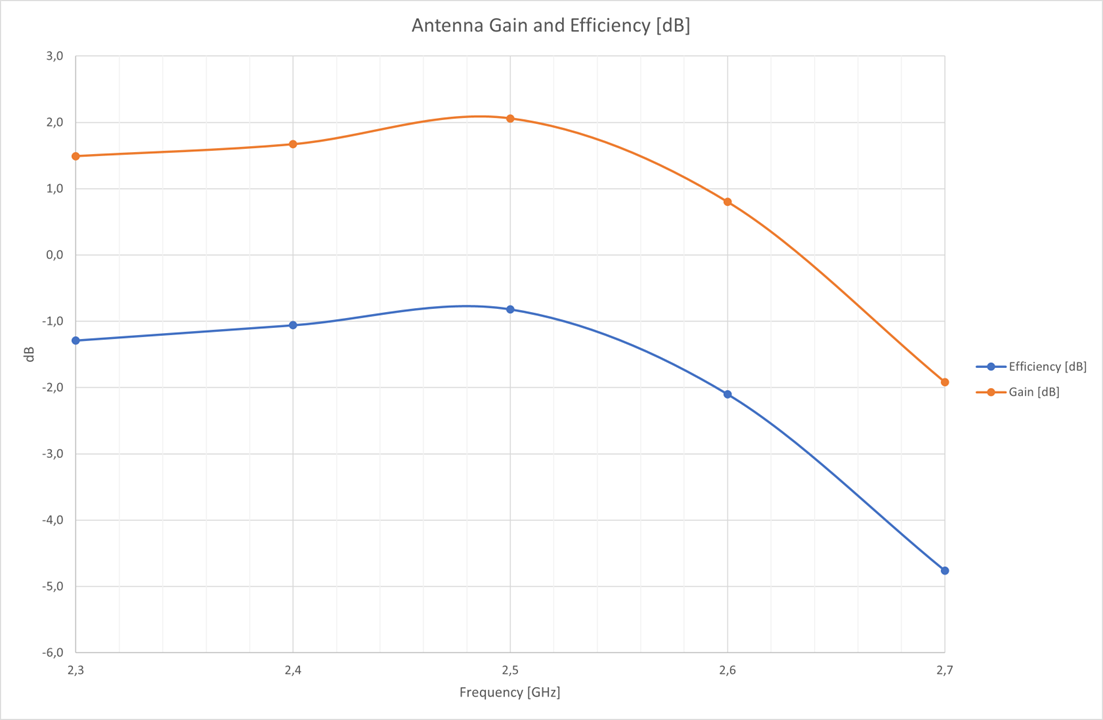
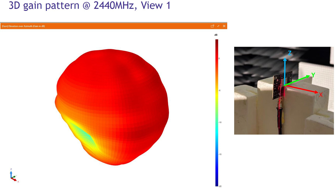
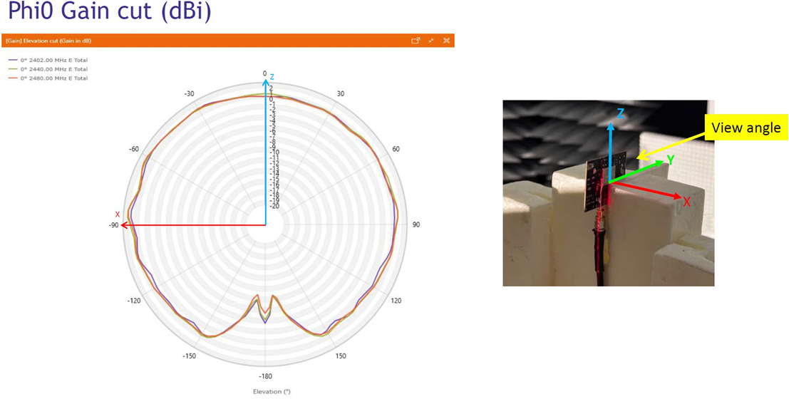
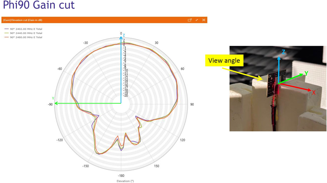
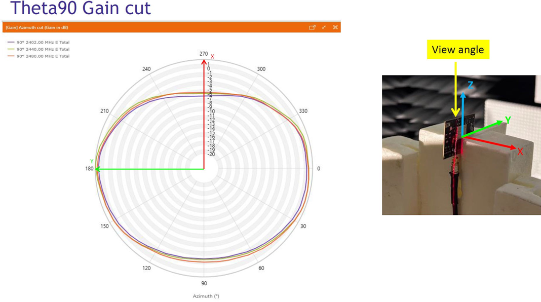
SL917 Integrated Antenna (453-00221) Antenna Radiation and Efficiency
Typical radiation patterns for the built-in antenna under optimal operating conditions are plotted in the figures that follow.
| Parameter | With optimal layout | Note |
|---|---|---|
| Efficiency | -1 dB | Antenna gain and radiation patterns have a strong dependence on the size and shape of the application PCB the module is mounted on, as well as on the proximity of any mechanical design to the antenna. Refer to Installation Guide for SL917 Integrated Antenna Module for recommendations to achieve optimal antenna performance. |
| Peak gain | 2.26 dBi |
PCB Layout
The figure below shows the recommended layout for SL917 NCP when using an RF connector (MHF4 recommended) for an external antenna. The short RF trace from the RF pad of the module to the pad of the RF connector must be 50 ohm and exactly the same width as the RF pad of the module, i.e., 700 μm. The figure below shows two examples on practical implementations of such a trace. The widths S is fixed to 700 um. The height h depends on the PCB stackup, and the gap width W is adjusted until the impedance of the trace is exactly 50 ohm. Online calculators for coplanar waveguide with ground can be used to calculate the width W for any specific PCB stack-up. The integrator must consider using a unique connector, such as a “reverse polarity SMA” or “reverse thread SMA”, if detachable antenna is offered with the host chassis.
Ground vias underneath the module must be used extensively especially around the rectangular GND pins to enable heat transfer from the bottom of the module to the GND plane of the host board. Routing signal lines elsewhere underneath the module is acceptable.
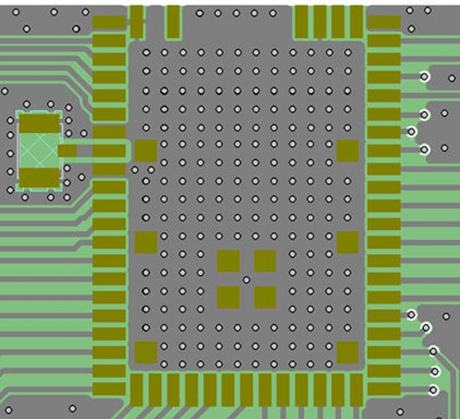
The typical permittivity of PCB laminate is 4.6. If assuming permittivity of 4.6, in the example shown below the dimensions would be:
S = 700 um
h = 420 um W = 332 um
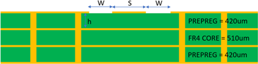
Similarly, if assuming permittivity of 4.6, in the example shown below the dimensions would be:
S = 700 um
h = 730 um W = 132 um
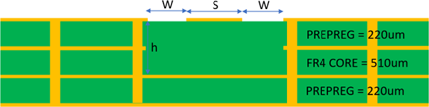
Antenna Integration
Installation Guide for SL917 Integrated Antenna NCP Module (453-00221)
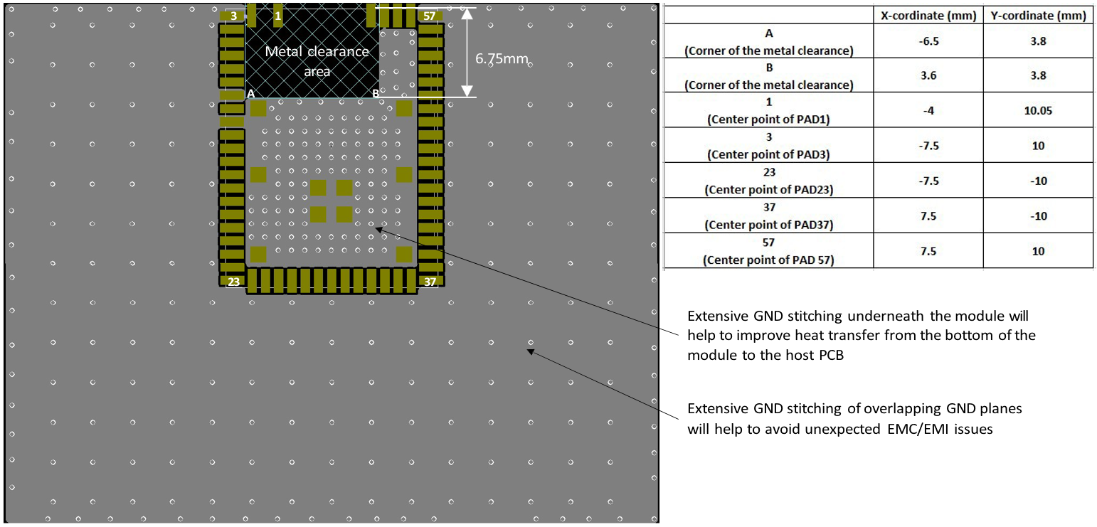
For optimal performance of the SL917 Integrated Antenna Module:
- Place the module aligned to the edge of the application PCB, as illustrated above.
- Leave the antenna clearance area void of any traces, components, or copper on all layers of the application PCB.
- Connect all ground pads directly to a solid ground plane.
- Place the ground vias as close to the ground pads as possible.
- Avoid plastic or any other dielectric material in direct contact with the antenna.
The following figure shows example layout scenarios which will lead to degraded performance and possible EMC issues with the module.
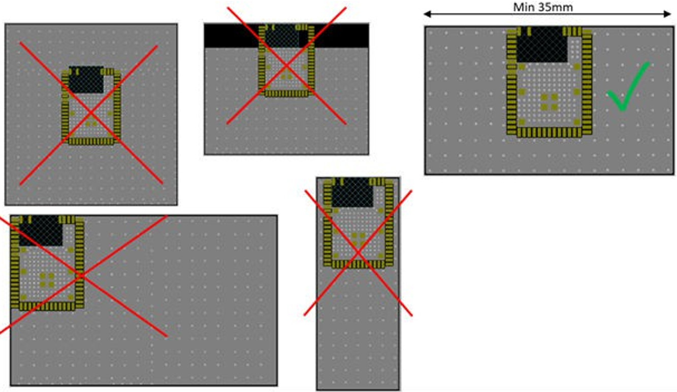
Ground vias underneath the module must be used extensively especially around the rectangular GND pins to enable heat transfer from the bottom of the module to the GND plane of the host board. Routing signal lines elsewhere underneath the module is acceptable.
Antennas are by nature affected by the surrounding PCB design and in particular the size and shape of the ground surrounding the antenna. The wide band antenna of SL917 Integrated Antenna module is designed to operate in various size/shape application boards and the antenna is not sensitive to dielectric material near the antenna. However, in certain extreme circumstances, such as extremely small board or narrow board, the antenna can be detuned enough to have an impact to the range, EVM characteristics and in-band emissions. In such cases it is possible to fine tune the antenna by using one or two external capacitors or inductors connected between the ANT_TUNE1 and GND and/or ANT_TUNE2 and GND. An example is shown below. Finding the correct value for these components requires empirical testing and measuring the antenna return loss. (See the note below on modular certification.)
The best antenna performance is achieved when the board width is 50mm and the antenna is placed at the center of the board edge. Having wider or narrower PCB will have up to 25% impact to the range. If the board is narrower than 35mm or wider than 100 mm, it is possible that external fine tuning becomes necessary to maintain the EVM performance.
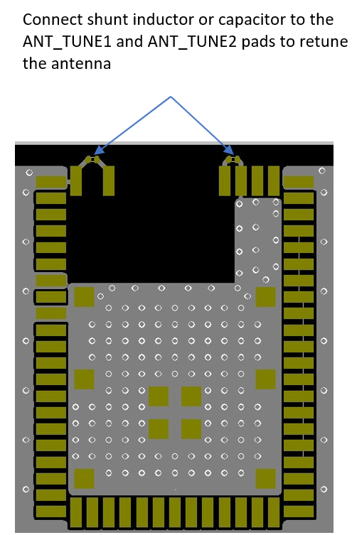
Application Note for Surface Mount Modules
Soldering Profile
It is recommended that final PCB assembly of the SL917 NCP Module follows the industry standard as identified by the Institute for Printed Circuits (IPC). This product is assembled in compliance with the J-STD-001 requirements and the guidelines of IPC-AJ-820. Surface mounting of this product by the end user is recommended to follow IPC-A-610 to meet or exceed class 2 requirements.
CLASS 1 General Electronic Products
Includes products suitable for applications where the major requirement is function of the completed assembly.
CLASS 2 Dedicated Service Electronic Products
Includes products where continued performance and extended life is required, and for which uninterrupted service is desired but not critical. Typically the end-use environment would not cause failures.
CLASS 3 High Performance/Harsh Environment Electronic Products
Includes products where continued high performance or performance-on-demand is critical, equipment downtime cannot be tolerated, end-use environment may be uncommonly harsh, and the equipment must function when required, such as life support or other critical systems.
Note: General SMT application notes are provided in AN1223: LGA Manufacturing Guidance.
Shipping and Labeling
Packaging
Tape and Reel
The SL917 NCP modules are delivered to the customer in cut tape (100 pcs) or reel (1000 pcs) packaging having the dimensions below. All dimensions are given in mm unless otherwise indicated.
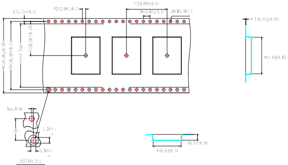
Environmental and Reliability
Environmental Requirements
Moisture Sensitivity Level
SL917 NCP modules are rated MSL3 (Moisture Sensitivity Level 3). Reels are delivered in packing which conforms to MSL3 requirements.
Regulatory, Qualification & Certifications
Regulatory Approvals
Note: For complete regulatory information, refer to the Veda SL917 Regulatory Information Guide, available on the Veda SL917 product page.
The Veda SL917 holds current certifications in the following countries:
| Country/Region | Regulatory ID |
|---|---|
| USA (FCC) | SQG-SL917 |
| Canada (ISED) | 3147A-SL917 |
| UK (UKCA) | *No Regulatory ID required |
| EU | *No Regulatory ID required |
| China (SRRC) | PENDING |
| Japan (MIC) | PENDING |
| Taiwan (NCC) | PENDING |
| Korea (KC) | PENDING |
| Australia (AS) | *No Regulatory ID required |
| New Zealand (NZS) | *No Regulatory ID required |
Certified Antennas
The Veda SL917 NCP modules have been tested and certified for the use with respectively the built-in integral antenna and a reference external antenna attached to the module's RF pin denoted as RF_PORT. The intended antenna impedance is 50 Ω. Because these modules and their associated set of approved antennas has been certified by the FCC and Innovation, Science and Economic Development, Canada (ISED) as Modular Radios, the end user is authorized to integrate this module into an end-product and is solely responsible for the Unintentional Emissions levels produced by the end-product.
To uphold the Modular Radio certifications, the integrator of the module must abide by the PCB layout recommendations outlined in the following paragraphs. Any divergence from these recommendations will invalidate the modular radio certifications and require the integrator to re-certify the module and/or end-product.
Performance characteristics for the built-in antenna are presented in Antenna Characteristics. The details of the qualified external antenna(s) are summarized below. The qualified external antenna(s) is(are) meant to be directly connected to the module's RF pin, with no active/non-linear component(s) along the RF path in between.
| Manufacturer and Model | Type | Peak Gain | Impedance |
|---|---|---|---|
| TE Connectivity Ltd. (previously Linx Technologies Inc.), ANT-2.4-CW-CT-RPS | Connectorized Coaxial Dipole | +2.8 dBi | 50 Ω |
| Ezurio (Laird Connectivity) 001-0022 | FlexPIFA | +2.0 dBi | 50 Ω |
| Ezurio (Laird Connectivity) 001-0023 | FlexNOTCH | +2.0 dBi | 50 Ω |
| Ezurio (Laird Connectivity) EBL2400A1-10MH4L | NanoBlue | +2.0 dBi | 50 Ω |
| Ezurio (Laird Connectivity) EFG2401A3S-10MH4L | i-FlexPIFA Mini | +2.0 dBi | 50 Ω |
| Ezurio (Laird Connectivity) EFG2400A3S-10MH4L | i-FlexPIFA | +3.1 dBi | 50 Ω |
| Ezurio (Laird Connectivity) EFA2400A3S-10MH4L | mFlexPIFA | +2.0 dBi | 50 Ω |
Regulatory Statements
When using the module and the reference design that supports the off module MH4 connector(s), you may use a substitute antenna if it is of the same type and that the gain is less than or equal to the smallest gain for that type for each of the frequencies listed. The OEM is free to choose another vendor’s antenna of like type and equal or lesser gain as an antenna appearing in the table and still maintain compliance. Reference FCC Part 15.204(c)(4) for further information on this topic.
When using instead an external antenna of a different type (such as a chip antenna, a host PCB trace antenna, or a patch) or having non-similar in-band and out-of-band characteristics, but still with a gain less than or equal to the maximum gain listed in the table above, in principle it can be added to the existing modular grant/certificate by mean of a permissive change, for example with FCC and ISED. Typically, some radiated emission testing is demanded, but no modular or end-product re-certification is required. Please consult your certification house and/or a certification body and/or the module manufacturer for confirmation of the correct procedures and for any authorization to perform permissive changes.
On the other hand, all products designed to be used with an external antenna having more gain than the maximum gain listed in the table above are very likely to require a full new end-product certification. Since the exact permissive change or registration or re-certification procedure is chosen on a case-by-case basis, please consult your certification house and/or a certification body to understand the correct approach based on your unique design. You might also want or need to get in touch with Ezurio for any authorization letter that your certification body might ask for.
In countries applying the ETSI standards, where manufacturers issue a self-Declaration of Conformity before placing their end-products in the market, like in the EU countries (and in the UK), the radiated emissions are always evaluated with the end-product and the external antenna type is not critical, but antennas with higher gain may violate some of the EIRP regulatory limits.
For Japan, where compliance testing is done conductively, the allowed external antennas are listed in the certificate and/or test report(s). Any other external antenna will have to be formally added to the list of approved antennas by the certificate holder: in this case, please reach out to the module manufacturer to discuss such additions or consider certifying the end-product itself as an alternative.
Federal Communications Commission Interference Statement
This equipment has been tested and found to comply with the limits for a Class B digital device, pursuant to Part 15 of the FCC Rules. These limits are designed to provide reasonable protection against harmful interference in a residential installation. This equipment generates, uses and can radiate radiofrequency energy and, if not installed and used in accordance with the instructions, may cause harmful interference to radio communications. However, there is no guarantee that interference will not occur in a particular installation. If this equipment does cause harmful interference to radio or television reception, which can be determined by turning the equipment off and on, the user is encouraged to try to correct the interference by one of the following measures:
- Reorient or relocate the receiving antenna.
- Increase the separation between the equipment and receiver.
- Connect the equipment into an outlet on a circuit different from that to which the receiver is connected.
- Consult the dealer or an experienced radio/TV technician for help.
FCC Caution: Any changes or modifications not expressly approved by the party responsible for compliance could void the user's authority to operate this equipment.
This device complies with Part 15 of the FCC Rules. Operation is subject to the following two conditions: (1) This device may not cause harmful interference, and (2) this device must accept any interference received, including interference that may cause undesired operation.
Radiation Exposure Statement
This equipment complies with FCC radiation exposure limits set forth for an uncontrolled environment. This equipment should be installed and operated with minimum distances equal or above those being reported in Table 12.2. Minimum Separation Distances for SAR Evaluation Exemption.
This transmitter must not be co-located or operating in conjunction with any other antenna or transmitter.
Integration Instructions for Host Product Manufacturers
Applicable FCC rules to module: FCC Part 15.247
Summary of the specific operational use conditions:
This device is intended only for OEM integrators under the following condition:
The transmitter module may not be co-located with any other transmitter antenna.
If the condition above is met, further transmitter test will not be required. However, the OEM integrator is still responsible for testing their end-product for any additional compliance requirements required with this module installed.
IMPORTANT NOTE: If these conditions cannot be met (for example certain laptop configurations or co-location with another transmitter), then the FCC authorization is no longer considered valid, and the FCC ID cannot be used on the final product. In these circumstances, the OEM integrator will be responsible for re-evaluating the end-product (including the transmitter) and obtaining a separate FCC authorization. The OEM integrator must be aware not to provide information to the end user regarding how to install or remove this RF module in the user’s manual of the end-product which integrates this module.
The end user manual shall include all required regulatory information/warning as shown in this manual.
Limited module procedures
Not applicable
RF exposure considerations
Co-located issue shall be met as mentioned in Summary of the specific operational use conditions.
Product manufacturer shall provide the following text in the end-product manual:
FCC Radiation Exposure Statement
The product complies with the US portable RF exposure limit set forth for an uncontrolled environment and are safe for intended operation as described in this manual. The further RF exposure reduction can be achieved if the product can be kept as far as possible from the user body or set the device to lower output power if such function is available.
A 5.5-centimeter separation distance and co-located issue shall be met as mentioned in Summarize the specific operational use conditions.
Product manufacturer shall provide the following text in the end-product manual:
This equipment complies with FCC radiation exposure limits set forth for an uncontrolled environment. This equipment should be installed and operated with a minimum distance of 5.5 centimeters between the radiator and your body.
Label and Compliance Information
Product manufacturers must provide, with the finished product, a physical or e-label that states the following:
Contains FCC ID: SQG-SL917
Additional Testing, Part 15 Subpart B Disclaimer
The module is only FCC authorized for the specific rule parts listed on the grant, and that the host product manufacturer is responsible for compliance to any other FCC rules that apply to the host not covered by the modular transmitter grant of certification. The final host product still requires Part 15 Subpart B compliance testing with the modular transmitter installed.
Applicable ISED rules to module: RSS-247
This device contains licence-exempt transmitter(s)/receiver(s) that comply with Innovation, Science and Economic Development Canada’s licence-exempt RSS(s). Operation is subject to the following two conditions:
(1) This device may not cause interference
(2) This device must accept any interference, including interference that may cause undesired operation of the device.
L’émetteur/récepteur exempt de licence contenu dans le présent appareil est conforme aux CNR d’Innovation, Sciences et Développement économique Canada applicables aux appareils radio exempts de licence. L’exploitation est autorisée aux deux conditions suivantes :
(1) L’appareil ne doit pas produire de brouillage;
(2) L’appareil doit accepter tout brouillage radioélectrique subi, même si le brouillage est susceptible d’en compromettre le fonctionnement.
This radio transmitter (IC: 3147A-SL917) has been approved by Innovation, Science and Economic Development Canada to operate with the antenna types listed in Table 12.1 above, with the maximum permissible gain indicated. Antenna types not included in this list that have a gain greater than the maximum gain indicated for any type listed are strictly prohibited for use with this device.
Le présent émetteur radio (IC: 3147A-SL917) a été approuvé par Innovation, Sciences et Développement économique Canada pour fonctionner avec les types d'antenne énumérés ci ci-dessus dans le tableau 4 et ayant un gain admissible maximal. Les types d'antenne non inclus dans cette liste, et dont le gain est supérieur au gain maximal indiqué pour tout type figurant sur la liste, sont strictement interdits pour l'exploitation de l'émetteur.
Radiation Exposure Statement:
This equipment complies with Canada radiation exposure limits set forth for an uncontrolled environment. This equipment should be installed and operated with minimum distance 3.5cm between the radiator & your body.
Déclaration d'exposition aux radiations:
Cet équipement est conforme Canada limites d'exposition aux radiations dans un environnement non contrôlé. Cet équipement doit être installé et utilisé à distance minimum de 3.5cm entre le radiateur et votre corps.
This device is intended only for OEM integrators under the following conditions:
- The transmitter module may not be co-located with any other transmitter or antenna.
As long as the condition above is met, further transmitter testing is not required. However, the OEM integrator is still responsible for testing their end-product for any additional compliance requirements required with this module installed.
Cet appareil est conçu uniquement pour les intégrateurs OEM dans les conditions suivantes:
- Le module émetteur peut ne pas être coïmplanté avec un autre émetteur ou antenne.
Tant que les 1 condition ci-dessus sont remplies, des essais supplémentaires sur l'émetteur ne seront pas nécessaires. Toutefois, l'intégrateur OEM est toujours responsable des essais sur son produit final pour toutes exigences de conformité supplémentaires requis pour ce module installé.
IMPORTANT NOTE: If these conditions cannot be met (for example certain laptop configurations or co-location with another transmitter), then the Canada authorization is no longer considered valid, and the IC ID cannot be used on the final product. In these circumstances, the OEM integrator will be responsible for re-evaluating the end product (including the transmitter) and obtaining a separate Canada authorization.
NOTE IMPORTANTE: Dans le cas où ces conditions ne peuvent être satisfaites (par exemple pour certaines configurations d'ordinateur portable ou de certaines co-localisation avec un autre émetteur), l'autorisation du Canada n'est plus considéré comme valide et l'ID IC ne peut pas être utilisé sur le produit final. Dans ces circonstances, l'intégrateur OEM sera chargé de réévaluer le produit final (y compris l'émetteur) et l'obtention d'une autorisation distincte au Canada.
End Product Labelling
The end product must be labelled in a visible area with the following: “Contains IC: 3147A-SL917”.
Plaque signalétique du produit final
Le produit final doit être étiqueté dans un endroit visible avec l'inscription suivante: "Contient des IC: 3147A-SL917.
Manual Information to the End User
The OEM integrator must be aware not to provide information to the end user regarding how to install or remove this RF module in the user’s manual of the end product which integrates this module.
The end user manual shall include all required regulatory information/warning as show in this manual.
Manuel d'information à l'utilisateur final
L'intégrateur OEM doit être conscient de ne pas fournir des informations à l'utilisateur final quant à la façon d'installer ou de supprimer ce module RF dansle manuel de l'utilisateur du produit final qui intègre ce module.
Le manuel de l'utilisateur final doit inclure toutes les informations réglementaires requises et avertissements comme indiqué dans ce manuel.
RF Exposure and Proximity to the Human Body
When using the Veda SL917 modules in an application where the radio-equipped end-product is located close to the human body, the human RF Exposure must be considered. FCC, ISED, and CE/UKCA all have different standards and rules for evaluating the RF Exposure. Each regulator has different requirements when it comes to the exemption from having to perform RF Exposure and SAR (Specific Absorption Rate) measurements, and the minimum separation distances between the module's antenna and the human body varies accordingly. The properties of the Veda SL917 modules allow the minimum separation distances detailed in the table below for the SAR evaluation exemption in the Portable use cases (less than 20 cm from the human body). These modules are approved for the Mobile use case (more than 20 cm) without any need for RF Exposure evaluation.
| Certification | Veda SL917 |
|---|---|
| USA (FCC) | Wi-Fi 802.11b/g/n/ax: 55 mm BLE: 10 mm |
| Canada (ISED) | Wi-Fi 802.11b/g/n/ax: 35 mm BLE: 20 mm |
| EU (CE) / UK (UKCA) | The RF exposure should always be evaluated with the end-product when transmitting with EIRP power levels higher than 20 mW (13 dBm) while at a closer than 20cm distance from the human body. With the Veda SL917 modules, this is the case only with the 802.11b/g/n/ax protocols operating at full power, in particular when the distance is TBD cm and below. In all other cases, modules comply with the requirements of the relevant standard(s) |
Bluetooth SIG Qualification
The Bluetooth Qualification Process promotes global product interoperability and reinforces the strength of the Bluetooth® brand and ecosystem to the benefit of all Bluetooth SIG members. The Bluetooth Qualification Process helps member companies ensure their products that incorporate Bluetooth technology comply with the Bluetooth Patent & Copyright License Agreement and the Bluetooth Trademark License Agreement (collectively, the Bluetooth License Agreement) and Bluetooth Specifications.
The Bluetooth Qualification Process is defined by the Qualification Program Reference Document (QPRD) v3.
To demonstrate that a product complies with the Bluetooth Specification(s), each member must for each of its products:
- Identify the product, the design included in the product, the Bluetooth Specifications that the design implements, and the features of each implemented specification
- Complete the Bluetooth Qualification Process by submitting the required documentation for the product under a user account belonging to your company
The Bluetooth Qualification Process consists of the phases shown below:

To complete the Qualification Process the company developing a Bluetooth End Product shall be a member of the Bluetooth SIG. To start the application please use the following link: Apply for Adopter Membership
Scope
This guide is intended to provide guidance on the Bluetooth Qualification Process for End Products that reference multiple existing designs, that have not been modified, (refer to Section 3.2.2.1 of the Qualification Program Reference Document v3).
For a Product that includes a new Design created by combining two or more unmodified designs that have DNs or QDIDs into one of the permitted combinations in Table 3.1 of the QPRDv3, a Member must also provide the following information:
- DNs or QDIDs for Designs included in the new Design
- The desired Core Configuration of the new Design (if applicable, see Table 3.1 below)
- The active TCRL Package version used for checking the applicable Core Configuration (including transport compatibility) and evaluating test requirements
Any included Design must not implement any Layers using withdrawn specification(s).
When creating a new Design using Option 2a, the Inter-Layer Dependency (ILD) between Layers included in the Design will be checked based on the latest TCRL Package version used among the included Designs.
For the purposes of this document, it is assumed that the member is combining unmodified Core-Controller Configuration and Core-Host Configuration designs, to complete a Core-Complete Configuration.
Qualification Steps When Referencing multiple existing designs, (unmodified) – Option 2a in the QPRDv3
For this qualification option, follow these steps:
- To start a listing, go to: https://qualification.bluetooth.com/
- Select Start the Bluetooth Qualification Process.
Product Details to be entered:
- Project Name (this can be the product name or the Bluetooth Design name).
- Product Description
- Model Number
- Product Publication Date (the product publication date may not be later than 90 days after submission)
- Product Website (optional)
- Internal Visibility (this will define if the product will be visible to other users prior to publication)
- If you have multiple End Products to list then you can select ‘Import Multiple Products’, firstly downloading and completing the template, then by ‘Upload Product List’. This will populate Qualification Workspace with all your products.
Specify the Design:
- Do you include any existing Design(s) in your Product? Answer Yes, I do.
- Enter the multiple DNs or QDIDs used in your, (for Option 2a two or more DNs or QDIDs must be referenced)
- Select ‘I’m finished entering DN’s
- Once the DNs or QDIDs are selected they will appear on the left-hand side, indicating the layers covered by the design (should show Core-Controller and Core Host Layers covered).
- What do you want to do next? Answer, ‘Combine unmodified Designs’.
- The Qualification Workspace Tool will indicate that a new Design will be created and what type of Core-Complete configuration is selected.
- An active TCRL will be selected for the design.
- Perform the Consistency Check, which should result in no inconsistencies
- If there are any inconsistencies these will need to be resolved before proceeding
- Save and go to Test Plan and Documentation
Test Plan and Documentation
- As no modifications have been made to the combined designs the tool should report the following message:
‘No test plan has been generated for your new Design. Test declarations and test reports do not need to be submitted. You can continue to the next step.’ - Save and go to Product Qualification fee
- As no modifications have been made to the combined designs the tool should report the following message:
Product Qualification Fee:
- It’s important to make sure a Prepaid Product Qualification fee is available as it is required at this stage to complete the Qualification Process.
- Prepaid Product Qualification Fee’s will appear in the available list so select one for the listing.
- If one is not available select ‘Pay Product Qualification Fee’, payment can be done immediately via credit card, or you can pay via Invoice. Payment via credit will release the number immediately, if paying via invoice the number will not be released until the invoice is paid.
- Once you have selected the Prepaid Qualification Fee, select ‘Save and go to Submission’
Submission:
- Some automatic checks occur to ensure all submission requirements are complete.
- To complete the listing any errors must be corrected
- Once you have confirmed all design information is correct, tick all of the three check boxes and add your name to the signature page.
- Now select ‘Complete the Submission’.
- You will be asked a final time to confirm you want to proceed with the submission, select ‘Complete the Submission’.
- Qualification Workspace will confirm the submission has been submitted. The Bluetooth SIG will email confirmation once the submission has been accepted, (normally this takes 1 working day).
Download Product and Design Details (SDoC):
- You can now download a copy of the confirmed listing from the design listing page and save a copy in your Compliance Folder
For further information, please refer to the following webpage:
https://www.bluetooth.com/develop-with-bluetooth/qualification-listing/
Example Design Combinations
The following gives an example of a possible design under option 2a:
Ezurio Core Controller + Zephyr Core Host Software Stack (Ezurio Veda SL917-based design)
| Design Name | Listing Type | Owner | Declaration ID | QD ID / DN | Link to listing on the SIG website |
| Veda SL917 | Core Controller | Ezurio | N/A | Q382245 | https://qualification.bluetooth.com/ListingDetails/324124 |
| Simplicity SDK for Zephyr v2025.12.0 and above | Core Host | Silicon Laboratories | N/A | Q379004 | https://qualification.bluetooth.com/ListingDetails/321296 |
An alternative Core Host option is listed below, select only one Core Host for your new design:
| Design Name | Listing Type | Owner | Declaration ID | QD ID / DN | Link to listing on the SIG website |
| SiWx91x Host Subsystem based on Core Specification 5.4 | Core Host | Silicon Laboratories | D066772 | 226680 | https://qualification.bluetooth.com/ListingDetails/93911 |
Qualify More Products
If you develop further products based on the same design in the future, it is possible to add them free of charge. The new product must not modify the existing design i.e add ICS functionality, otherwise a new design listing will be required.
To add more products to your design, select ‘Manage Submitted Products’ in the Getting Started page, Actions, Qualify More Products. The tool will take you through the updating process.
Ordering Information
| Part # | Description |
|---|---|
| 453-00219R | Module, Veda SL917, 4MB Flash, NCP, Trace Pad, Tape and Reel |
| 453-00219C | Module, Veda SL917, 4MB Flash, NCP, Trace Pad, Cut Tape |
| 453-00221R | Module, Veda SL917, 4MB Flash, NCP, Integrated Antenna, Tape and Reel |
| 453-00221C | Module, Veda SL917, 4MB Flash, NCP, Integrated Antenna, Cut Tape |
Veda Click Boards (from MIKROE.com)
| Part # | Description | Link |
|---|---|---|
| Veda SL917 Click (Integrated Antenna) | Click Board - Veda SL917 NCP Module – Integrated Antenna | See at MIKROE.com |
| Veda SL917 Click (RF Trace Pad or External Antenna) | Click Board - Veda SL917 NCP Module – RF Trace Pad + FlexPIFA (MHF4) | See at MIKROE.com |
Legacy - Revision History
| Version | Date | Notes | Contributors | Approver |
|---|---|---|---|---|
| 0.7 | 19 Feb 2025 | Initial Release | Dave Drogowski Dave Neperud | Andy Ross |
| 0.8 | 2 May 2025 | Added sections 12.1 – 12.4 on qualified Ezurio antennas, FCC, ISED, and RF exposure statements | Dave Neperud |
Preliminary Revision History
Revision 0.7
November, 2024
- Updated Cover page
- Updated 1. Feature List
- Updated 3. Applications
- Removed Host Interfaces
- Updated 6.2 Pin Description
- Updated 6.2.3 Peripheral Interfaces
- Updated the following Electrical Specifications:
- Removed UART
- Removed SGPIO/MC-PWM/QEI/SCT Timer/SIO Interfaces and USART
- Added Note to 8.4.2 Proximity to Human Body
Revision 0.52
October, 2024
- Updated Notes for 1. Feature List
- Updated 2. Ordering Information
- Reformatted all the tables in Section
- Updated Section 7.5 RF Characteristics
- Updated 12.11 Bluetooth Qualification
Revision 0.5
June, 2024
- Updated Features List
- Updated Ordering Information
- Updated Block Diagrams
- Updated System Overview
- Updated Pin Definitions
- Updated Electrical Specifications
- Updated Reference Schematics, BOM and Layout Guidelines
- Added Certifications
Revision 0.1
September, 2023
- Preliminary version.