/filters:background_color(white)/2025-01/453-00219%20front4.416.png)
Introduction
Overview
This document describes key hardware aspects of the Veda SL917 SoC Module. This document is intended to assist device manufacturers and related parties with the integration of this radio into their host devices. Data in this document is drawn from several sources. For full documentation on the Veda SL917, visit:
https://www.ezurio.com/veda-sl917
General Description
Ezurio’s SL917 module is our lowest power Wi-Fi 6 plus Bluetooth LE 5.4, ideal for ultra-low power IoT wireless devices using Wi-Fi®, Bluetooth, Matter, and IP networking for secure cloud connectivity. It is optimal for developing battery operated devices that need long battery life. The SL917 SoC module includes an ultra-low power Wi-Fi 6 plus Bluetooth Low Energy (LE) 5.4 wireless CPU subsystem, and an integrated micro-controller (MCU) application subsystem, security, peripherals and power management sub- system all in a single 16 x 21.1 x 2.3 mm package. The wireless subsystem consists of a multi-threaded Network Wireless Processor (NWP) running up to 160 MHz, baseband digital signal processing, analog front end, 2.4 GHz RF transceiver and integrated power amplifier. The application subsystem consists of an ARM® Cortex®-M4 running up to 180 MHz, embedded SRAM, FLASH, ultra-low power sensor hub, and matrix vector processor. The ARM® Cortex®-M4 is dedicated for peripheral and application-related processing, while the NWP runs the wireless and networking stacks on independent threads, thus providing a fully integrated solution that is ready for a wide range of embedded wireless IoT applications. The modules come with modular radio type approvals for various countries, including USA (FCC), Canada (IC/ISED) and Japan (MIC), and are in compliance with the relevant EN standards (including EN 300 328 v2.2.2) for the conformity with the directives and regulations in EU and UK.
This datasheet is subject to change. Please contact Ezurio for further information.
Application Areas
- Smart Home
- Security cameras
- HVAC
- Smart Sensors
- Smart Appliances
- Health and Fitness
- Pet Trackers
- Smart Cities
- Smart Meters
- Industrial Wearables
- Smart Buildings
- Asset Tracking
- Smart hospitals
Features & Benefits
The Veda SL917 SoC device features and benefits are described below.
- Wi-Fi 6 Single Band 2.4 GHz 20 MHz 1x1 stream IEEE 802.11 b/g/n/ax
- Bluetooth LE 5.4
- Single chip Matter Over Wi-Fi Solution
- ARM® Cortex® M4 Processor with FPU subsystem up to 180 MHz with rich set of Digital and Analog Peripherals.
- Wi-Fi 6 Benefits: TWT for improved efficiency and longer battery life, MU- MIMO/OFDMA for Higher Throughput, network capacity and low latency
- Best in Class Device and Wireless Security
- WLAN Tx power up to +17.5 dBm with integrated PA
- Bluetooth LE Tx power up to +17 dBm with integrated PA
- WLAN Rx sensitivity as low as -95 dBm
- Wi-Fi Standby Associated mode current: 78 μA @ 1-second listen interval
- Embedded Flash option up to 8 MB/ optional external Flash up to 16 MB
- Embedded PSRAM option up to 8 MB/ optional external PSRAM option up to 16 MB
- Ultra-low power sensor hub peripherals
- Matrix Vector Processor (MVP)
- Embedded Wi-Fi, Bluetooth LE, Matter, and networking stacks supporting wireless coexistence
- Three software-configurable MCU application memory options for sharing the RAM between the wireless, system, and application (192/256/320 KB)
- Operating temperature: -40 ºC to +85 ºC
- Operating supply range: 3.0 V - 3.63 V
- Supply voltage for GPIOs: 1.71 V to 3.63 V
Specification Summary
Processor / SoC / Chipset
| MCU |
|
| Matrix Vector Processor (MVP) |
|
Wi-Fi
| Standards |
|
| Wi-Fi Features |
|
| Frequency Range |
|
| Spatial Streams |
|
| Channel Support |
|
| Supported Data Rates |
|
| Max Transmit Power |
|
| Receive Sensitivity |
|
| Operating Modes |
|
| Embedded Wi-Fi Stack |
|
| Coexistence |
|
Bluetooth
| Standards |
|
| Bluetooth Features |
|
| Frequency Range |
|
| Max Transmit Power |
|
| Min Transmit Power |
|
| Bluetooth Stack |
|
Radio Performance
| RF and Modem Features |
|
Interfaces
| Memory Interfaces |
|
| Ultra-Low Power Sensor Hub System |
|
| Peripheral Interface | 43x Multifunction I/O lines |
|---|---|
| USART |
|
| UART |
|
| GPIO |
|
| PWM |
|
| SSI/SPI |
|
| SDIO |
|
| TEMP |
|
| I2C |
|
| I2S |
|
| QEI |
|
| COMP |
|
| Touch Sensor |
|
| Timers |
|
| ADC |
|
| DAC |
|
| Op-Amp |
|
| Ultra Low Power (ULP) Peripherals |
Power
| Operating Supply Voltage | 3.0 V to 3.63 V |
| GPIO Supply Voltage | 1.71 V to 3.63 V |
| Power Consumption | MCU Sub-System:
Wireless Sub-System
|
| Power Management |
|
Mechanical
| Dimensions |
|
Software
| Security |
|
| Advanced Features |
|
Environmental
| Operating Temperature | -40 ºC to +85 ºC |
| MSL (Moisture Sensitivity Level) | 3 |
| Lead Free | Lead-free and RoHS Compliant |
Certifications
| Regulatory Compliance |
|
| Bluetooth SIG |
|
| Wi-Fi Alliance |
|
| Matter |
|
Development
| WiSeConnect SDK Features |
|
Warranty
| Warranty Terms | One Year Warranty |
Notes:
- For information about software roadmap features, and lists of available features and profiles, contact Ezurio or refer to Release Notes and Reference Manual.
- All power and performance numbers are under ideal conditions.
- For information about software roadmap features and additional certification information, contact Ezurio for availability and timeline. All available certifications and test reports will be posted in the Certifications section of the SL917 product page, and are documented in the SL917 Regulatory Information Guide.
Functional Descriptions
System Overview
The SL917 Modules include two processors: An ARM Cortex-M4 running up to 180 MHz and a Network Wireless Processor (NWP) 4-Threaded processor running up to 160 MHz. The Cortex-M4 is dedicated for peripheral and application related processing, whereas all the networking and wireless stacks run on independent threads of the NWP. In addition, in adherence to the Secure Execution Environment architecture, the NWP subsystem also acts as the secure processing domain and takes care of secure boot, secure firmware update, and provides access to security accelerators and secure peripherals through pre-defined APIs. The bus matrices of a Cortex M4 and NWP are separate and asynchronous. Though the two processors are present in a single chip, it is ensured that the NWP Networking, Security, and Wireless subsystem is completely separated from the ARM Cortex-M4 based application subsystem. Thus, these two processors have separate power, clocks/PLLs, bus-matrices, and memory. This provides two key advantages: programming, operating and power-state independence between the two processors and enhanced security by restricting access to the NWP subsystem.
SL917 modules are based on Silicon Labs’ SiWG917M ultra-low-power, single spatial stream, 802.11 b/g/n/ax + BLE 5.4 Convergence SoC. The SL917 module provides low-cost CMOS integration of a multi-threaded MAC processor, baseband digital signal processing, analog front-end, crystal oscillator, calibration eFuse, 2.4GHz RF transceiver, integrated power amplifier, matching network, bandpass filter (BPF), and Quad-SPI Flash thus providing a fully-integrated solution for a range of hosted and embedded wireless applications. With Silicon Labs' embedded four-threaded processor and on-chip ROM and RAM, these chipsets enable integration into low cost and zero host load applications. With an integrated PMU and support for a variety of digital peripherals, SL917 modules enable very low-cost implementations for wireless hosted and embedded applications. It can be connected to a host processor through SDIO, SPI or UART interfaces. Wireless firmware upgrades and provisioning are supported.
ARM Cortex M4
The ARM Cortex-M4 is the main application processor in the SiWG917M embedded SoC. It is a high-performance 32-bit processor designed by ARM for the microcontroller market. It is built on a high-performance processor core, with a 3-stage pipeline Harvard architecture, making it ideal for demanding embedded applications. The M4 processor delivers exceptional power efficiency through an efficient instruction set and extensively optimized design, providing high-end processing hardware including IEEE754-compliant single-precision floating-point computation, a range of single-cycle and Single Instruction Multiple Data (SIMD) multiplication and multiply-with- accumulate capabilities, saturating arithmetic and dedicated hardware division. The Cortex M4 microcontroller integrated into SiWG917M embedded SoC supports the following features:
- MPU (Memory Protection Unit) with 8 memory regions, FPU (Floating Point Unit), and NVIC (Nested Vectored Interrupt Controller) with 64 levels of interrupt priority
- Debug port with both JTAG as well as Serial Wire Debug (SWD) interface; comprehensive debug functionality including data matching for a watch-point generation
- To provide optimal power vs performance tradeoff, unique gear-shifting is available for the Cortex-M4 that enables optimal power consumption based on the required performance. The available power-states are Power State 4 (PS4) at up to 180 MHz, Power State 3 (PS3) at up to 90 MHz, and Power State 2 (PS2) at up to 32 MHz. More details are provided in Section 5.5.4 Power States .
- Architectural clock gates are included to minimize dynamic power dissipation.
- The Network Wireless Processor and Cortex-M4 communicate through thread to thread interrupting and memory.
- On-chip M4 SRAM of 192/256/320 KB based on the SiWG917M embedded SoC chip configuration
- 8 KB is present in the ultra-low-power (ULP) peripheral subsystem. This memory is present on the S-bus of the Cortex-M4 and is primarily used by the ULP MCU peripherals like ULP I2S, etc.
- 64 KB of ROM which hold the Cortex-M4 peripheral drivers
- 16 KB of instruction cache enabling eXecute In Place (XIP) with external quad/octal SPI Single Data Rate (SDR) flashes
- Based on the SiWG917M embedded SoC package configuration, up to 8 MB of in-package Quad Serial Peripheral Interface (QSPI) flash is available for the Cortex-M4. This flash can be shared with the NWP in common flash mode.
- eFuse of 32 bytes (available for customer applications)
- 225 Dhrystone million instructions per second (DMIPS) performance
The Cortex-M4 core includes the following core peripherals:
Nested Vectored Interrupt Controller
The NVIC is an embedded interrupt controller that supports low latency interrupt processing.
Memory Protection Unit
The memory protection unit (MPU) improves system reliability by defining the memory attributes for different memory regions. It pro- vides up to eight different regions and an optional predefined background region. It provides fine-grain memory control, enabling applications to utilize multiple privilege levels, separating and protecting code, data, and stack on a task-by-task basis. Such requirements are becoming critical in many embedded applications such as automotive.
The memory map and the programming of the MPU split the memory map into regions. Each region has a defined memory type, and some regions have additional memory attributes. The memory type and attributes determine the behavior of accesses to the region.
The memory types are:
- Normal: The M4 processor can re-order transactions for efficiency, or perform speculative reads.
- Device: The M4 processor preserves transaction order relative to other transactions to device or strongly-ordered memory.
- Strongly-ordered: The M4 processor preserves transaction order relative to all other transactions. The different ordering requirements for device and strongly-ordered memory mean that the memory system can buffer a write to device memory, but must not buffer a write to strongly-ordered memory.
The additional memory attributes include:
- Shareable: For a shareable memory region, the memory system provides data synchronization between bus primaries in a system with multiple bus primaries, for example, a M4 processor with a Direct Memory Access (DMA) controller. Strongly-ordered memory is always shareable. If multiple bus primaries can access a non-shareable memory region, the software must ensure data coherency between the bus primaries.
- Execute Never (XN): Means the M4 processor prevents instruction accesses. A fault exception is generated only on execution of an instruction executed from an XN region.
Floating-Point Unit
The Floating-point unit (FPU) provides IEEE754-compliant operations on single-precision, 32-bit, floating-point values. It supports addition, subtraction, multiplication, division and square root.
Memory Architecture
There are on chip Read Only Memory (ROM), Random Access Memory (RAM) and off chip FLASH connectivity. Sizes of ROM/RAM/ FLASH will vary depending on the chip configuration.
Highlights:
- Unified memory architecture - software can partition the memory between code and data usage
- Multiport - RAMs support multi port access - allowing simultaneous access from different primaries (I, D, DMAs) to non overlapping regions without any cycle penalty
- ROM/RAMs are tightly coupled to the M4 processor I/D buses to reduce the latency and power
- Supports memory protection - generates trap if unintended primary accesses the memory
The Cortex-M4 processor has following memory:
- On-chip M4 SRAM of 192/256/320 KB based on the chip configuration
- 8 KB is present in the Ultra-low-power(ULP) peripheral subsystem. This memory is present on the S-bus of the Cortex-M4 and is primarily used by the ULP MCU peripherals like ULP I2S, ADC, DAC etc.
- 64 KB of ROM which holds the M4 peripheral drivers and bootloader.
- 16 KB of Instruction cache (I cache) enabling eXecute In Place (XIP) with external quad/octal SPI SDR flashes.
- Based on the package configuration up to 8 MB of "in-package" Quad SPI flash is available for the M4. This flash can be shared with the NWP in common flash mode
- eFuse of 32 bytes (available for customer applications)
- 16 KB of Data cache (D cache) enabling data fetching with PSRAM and Instruction cache (I cache) to execute code from PSRAM
Flash Memory:
- Based on the package configuration (OPN) up to 8 MB of "in-package" Quad SPI flash is available.
In addition, IC can support external flash option
IC has the support for 2-flash configuration
- Common flash: Flash is common for both Cortex M4 and NWP
- Dual Flash: Separate flash can be used for Cortex M4 and NWP
Flash Architecture
Details for Flash Architecture are explained in the Flash Memory Section of the Reference Manual.
SRAM Memory Sharing between Cortex M4 and Network Wireless Processor
A configurable SRAM feature for different processors can reduce the total on-chip memory requirement while addressing the memory requirements for different product modes.
The 91x SoC architecture allows different memory sizes allocated to the Cortex M4 and NWP processors based on the chip configuration at bootup time. The allocated memory will run on the respective processor clock. Through the efficient hardware design, memory sizes are divided and accessible by multiple processors in a single cycle using tightly coupled interfaces (TCM).
On-chip SRAM memory can be allocated to the two processors in four chunks: 352 KB, 64 KB, 64 KB, and 192 KB. The 352 KB chunk is always allocated to the NWP processor while the 192 KB chunk is always allocated to the Cortex M4. The remaining two 64 KB chunks can be allocated to either the Cortex M4 or the NWP processor. For example, if the NWP processor requires more than 352 KB, and the M4 does not need all 320 KB, an additional 64 KB or 128 KB can be allocated to the NWP.
Thus the available options are for the NWP to use 352, 416, or 480 KB SRAM, with the M4 using 320, 256, or 192 KB of SRAM, respectively.
Memory configuration between the MCU and Wireless Sub-system is shown in Possible Memory Configurations between MCU and Wireless Sub-system.
The NWP and M4 memory architecture is shown below. NWPSS is the Network Wireless Processor subsystem and M4SS is the Cortex M4 subsystem.
Advanced Peripheral Bus (APB)
- The APB is part of the AMBA 3 protocol family.
- It provides a low-cost interface that is optimized for minimal power consumption and reduced interface complexity.
- The APB interfaces to any peripherals that are low-bandwidth and do not require the high performance of a pipelined bus interface.
- The APB has unpipelined protocol.
- All signal transitions are only related to the rising edge of the clock to enable the integration of APB peripherals easily into any design flow.
- Every transfer takes at least two cycles.
- It can be used to provide access to the programmable control registers of peripheral devices.
Interconnect
The following are the buses and bridges that form the interconnect in the SL917 module. MCU refers to the Cortex-M4, and NWP refers to the Network Wireless Processor.
- High Performance (HP) MCU AHB Interconnect Matrix (ICM)
- MCU AHB-to-APB dual bridge
- MCU AHB-to-ULP MCU synchronous AHB bridge
- ULP MCU AHB ICM
- ULP MCU AHB-to-APB bridge
- MCU AHB - NWP AHB bridge
- High Performance NWP AHB ICM
- NWP AHB-to-APB dual bridge
The High Performance MCU AHB ICM is a multilayer interconnect implementation of the AHB protocol designed for higher performance and higher frequency systems.
Address Mapping
The following are the base addresses of memories and high-speed peripherals.
MCU AHB Secondary Address Mapping
| Block Name | Size | Start Address |
|---|---|---|
| Memories | ||
| LP SRAM | 320 KB | 0x0000_0000 |
| ROM | 64 KB | 0x0030_0000 |
| AHB Peripherals | ||
| QSPI 1 Direct Access Mode | 32 MB | 0x0800_0000 |
| QSPI 1 Indirect Access Mode | 256 KB | 0x1200_0000 |
| QSPI 2 Direct Access Mode | 32 MB | 0x0A00_0000 |
| QSPI 2 Indirect Access Mode | 256 KB | 0X1204_0000 |
| SDIO/HSPI Secondary | 64 KB | 0x2020_0000 |
| Icache | 64 KB | 0x2028_0000 |
| GPDMA | 512 KB | 0x2108_0000 |
| ULPSS AHB Bridge | 256 KB | 0x2404_0000 |
| APB Bridge | 64 MB | 0x4400_0000 |
| NWP AHB Bridge | 512 MB | 0x0010_0000 / |
| 0x0040_0000 / | ||
| 0x0060_0000 / | ||
| 0x0400_0000 / | ||
| 0x1000_0000 / | ||
| 0x2010_0000 / | ||
| 0x2040_0000 / | ||
| 0x2100_0000 / | ||
| 0x2200_0000 / | ||
| 0x4000_0000 | ||
| MVP Secondary | 256 KB | 0x2400_0000 |
The following are the base addresses of all low-speed MCU peripherals.
MCU APB Peripherals Address Mapping
| Peripheral | Base Address |
|---|---|
| PERIPHERAL Power Domain | |
| UART0 (USART0 in asynchronous mode) | 0x4400_0000 |
| USART0 (USART0 in synchronous mode) | 0x4400_0100 |
| I2C0 | 0x4401_0000 |
| SSI_MST | 0x4402_0000 |
| UDMA | 0x4403_0000 |
| DCACHE | 0x4404_0000 |
| SSI_SLV | 0x4501_0000 |
| UART1 | 0x4502_0000 |
| GSPI | 0x4503_0000 |
| CONFIG_TIMER | 0x4506_0000 |
| CRC | 0x4508_0000 |
| HWRNG | 0x4509_0000 |
| I2C1 | 0x4704_0000 |
| I2S0 | 0x4705_0000 |
| QEI | 0x4706_0000 |
| MCPWM | 0x4707_0000 |
| Peripherals part of ALWAYS ON Domain | |
| VIC | 0x4611_0000 |
| ROM_PATCH | 0x4612_0200 |
| EGPIO | 0x4613_0000 |
| REG_SPI | 0x4618_0000 |
| PMU | 0x4600_0000 |
| PAD_CFG | 0x4600_4000 |
| MISC_CFG | 0x4600_8000 |
| EFUSE | 0x4600_C000 |
The following are the base addresses of all low-speed ULP MCU peripherals.
ULP MCU APB Peripherals Address Mapping
| Peripheral | Starting Address |
|---|---|
| ULP_I2C | 0x2404_0000 |
| ULP_I2S | 0x2404_0400 |
| SSI_ULP | 0x2404_0800 |
| IR | 0x2404_0C00 |
| ULP Config | 0x2404_1400 |
| ULP_UART | 0x2404_1800 |
| ULP_TIMER | 0x2404_2000 |
| Touch Sensor (CTS) | 0x2404_2C00 |
| AUX ADC DAC Controller | 0x2404_3800 |
| NPSS_APB | 0x2404_8000 |
| ULP_EGPIO | 0x2404_C000 |
| IPMU Reg Access SPI | 0x2405_0000 |
| ULP Memory | 0x2406_0000 |
| ULP_UDMA | 0x2407_8000 |
Power Architecture
The Power Control Hardware implements the control sequences for transitioning between different power states (Active/Standby/Sleep/ Shutdown) and the power control for different group of peripherals. In addition, wakeup from any of the Standby/Sleep/Shutdown states based on hardware events or peripheral interrupts is supported. The Standby and Shutdown states can be reached from Active mode only through a Wait for Interrupt (WFI) instruction. Wakeup from Standby/Sleep/Shutdown states is through a hardware event or interrupt (Peripheral or External).
Highlights
- Two integrated buck switching regulators enable efficient Voltage Scaling across wide operating mode currents.
- High performance and ultra-low-power MCU peripheral subsystems and buses.
- Multiple voltage domains with independent voltage scaling of each domain.
- Fine grained power-gating including peripherals, buses and pads, thereby reducing power consumption when the peripheral/buses/ pads are inactive.
- Multiple active states using "gear-shifting" approach based on processing requirements, thereby reducing power consumption for low-power applications.
- Flexible switching between different active states with controls from software.
- Hardware based wakeup from Standby/Sleep/Shutdown states.
- All the peripherals are clock gated by default, thereby reducing the power consumption in inactive state.
- Wakeup times are configurable by software before going into sleep.
Power Domains
All the applications, high-speed interfaces, and peripherals are segregated into multiple power domains to achieve lower current consumption when they are inactive. At reset, all the domains are powered ON.
The following table describes the different group of peripherals for which power is controlled through software.
| S.No | Section | Domain Name | Functionality of the Power Domain |
|---|---|---|---|
| 1 | APPLICATIONS | DEBUG_FPU | Debug Functionality for Cortex-M4, Floating Point Unit for Cortex-M4 |
| ROM | ROM Core/Interface | ||
| SRAM | SRAM Banks | ||
| 2 | HIGH SPEED INTERFACE | QSPI_ICACHE | Quad/Octal 1 SPI SDR Flash Interface and ICache for the Cortex-M4 Processor, QSPI2 PSRAM inter- face, DCACHE |
| 3 | HP-PERIPHERALS | PERI_EFUSE | SPI/Synchronous Serial Interface (SSI) Primary, I2C, USART, Micro-DMA Controller, UART, SPI/SSI Secondary, Generic-SPI Primary, Config Timer, Random-Number Generator, CRC Accelerator, I2C, I2S Primary/Secondary, QEI, MCPWM and EFUSE for configuration information , MVP |
| DMA | General Purpose DMA Controller | ||
| SDIO-SPI | SDIO 2.0 Secondary, HSPI Secondary. | ||
| 4 | HIGH SPEED FLASH MEMORY | FLASH-LDO | Low DropOut (LDO)-FL 1.8 for Flash Memory |
| 5 | HIGH-FREQ-PLL | PLL-REGISTERS | PLL Programming Registers for High frequency clocks. |
| 6 | ULP-PERIPHERALS | DMA | Micro-DMA Controller |
| ADC-DAC | ADC and DAC Controller | ||
| I2C | I2C Primary/Secondary | ||
| SSI | SPI/SSI Primary | ||
| UART | UART | ||
| TOUCH | Capacitive Touch Sensor Controller | ||
| TIMER | Timers | ||
| 7 | UULP-PERIPHERALS | WDT | Watch Dog Timer |
| TS | Temperature Sensor Controller | ||
| PS | Process Sensor Controller | ||
| RTC | Real-Time Clock, MCU System Real Time Clock (SYSRTC) | ||
| STORAGE-DOMAIN1 | Storage Flops - Set1. Contains 8 bytes | ||
| STORAGE-DOMAIN2 | Storage Flops - Set2. Contains 8 bytes | ||
| STORAGE-DOMAIN3 | Storage Flops - Set3. Contains 16 bytes | ||
| SLEEP-FSM | Finite State Machine (FSM) for Sleep/Wakeup | ||
| CLOCK-CALIB | Calibration block for Sleep Clock. | ||
| BBFFS | Programming Registers which can be retained during sleep. | ||
| DS-TIMER | DEEP SLEEP Timer. | ||
| TIMESTAMP | Timestamping Controller. | ||
| LP-FSM | Low-Power (LP) FSM | ||
| RETEN | Retention Flops which can be retained during sleep. | ||
| 8 | Analog-PERIPHERALS | Aux-ADC | Auxiliary ADC |
| Aux-DAC | Auxiliary DAC | ||
| BOD | Brown-Out Detector |
The SRAM is also segregated into multiple power domains to achieve lower current consumption per the memory requirement. The power for the SRAM domains in active states can be controlled in the following manners:
- Shut-Down Mode/Deepsleep without Retention Mode: SRAM domains as described in the following table can be powered down for unused SRAM sections. This is configurable on a bank granularity. The RAM contents of powered down sections are not retained.
- Deep-Sleep (Lower Power Consumption) Mode: No SRAM contents are retained in this mode, and the SRAM is not accessible in this state.
The following table describes the segregation of power domains for SRAM (328 KB).
| S.No | Section | Domain Name | Functionality of the Power Domain |
|---|---|---|---|
| 1 | LP-SRAM | LP-SRAM-1 | 4 KB of SRAM (1x Banks) |
| LP-SRAM-2 | 4 KB of SRAM (1x Banks) | ||
| LP-SRAM-3 | 4 KB of SRAM (1x Banks) | ||
| LP-SRAM-4 | 4 KB of SRAM (1x Banks) | ||
| LP-SRAM-5 | 16 KB of SRAM (1x Banks) | ||
| LP-SRAM-6 | 32 KB of SRAM (2x Banks) | ||
| LP-SRAM-7 | 64 KB of SRAM (4x Banks) | ||
| LP-SRAM-8 | 64 KB of SRAM (4x Banks) | ||
| LP-SRAM-9 | 64 KB of SRAM (4x Banks) | ||
| LP-SRAM-10 | 64 KB of SRAM (4x Banks) | ||
| 2 | ULP-SRAM | ULP-SRAM-1 | 2 KB of SRAM (1x Banks) |
| ULP-SRAM-2 | 2 KB of SRAM (1x Banks) | ||
| ULP-SRAM-3 | 2 KB of SRAM (1x Banks) | ||
| ULP-SRAM-4 | 2 KB of SRAM (1x Banks) |
Voltage Domain
All the applications, high-speed interfaces, and peripherals are segregated into multiple voltage domains to configure the operating voltages in different power states. This section describes the voltage domains and voltage source options available for each domain. These are configured based on the power state in which the device is operating. The voltage for each domain can be shut-off during sleep by configuring the source to SoC LDO (This supply is turned OFF during Sleep).
The following table lists the different voltage sources and the possible output voltages of each source at different power states.
| S.No | Voltage Source | Possible Output Voltage |
|---|---|---|
| 1 | SoC LDO | 1.15 V 1.05 V |
| 2 | SC-DC 1.05 | 1.05 V |
| 3 | LDO 0.75 V | 0.75 V |
The following table lists the different voltage domains and the possible voltage sources for each domain.
| S.No | Voltage Domain | Functionality | SoC LDO | SC-DC 1.05 V | LDO 0.75 V |
|---|---|---|---|---|---|
| 1 | PROC-DOMAIN | M4 processor, DEBUG_FPU, | Yes | Yes | Yes |
| 2 | HIGH-VOLTAGE-DOMAIN | ICACHE, HIGH-SPEED-INTERFACES, HP-PERIPHERALS, DCACHE | Yes | No | No |
| 3 | LOW-VOLTAGE-LPRAM-16KB | LP-SRAM-1, LP-SRAM-2, LP-SRAM-3, LP-SRAM-4, | Yes | Yes | No |
| 4 | LOW-VOLTAGE-LPRAM | ROM LP-SRAM-5, LP-SRAM-6, LP-SRAM-7, LP-SRAM-8, LP-SRAM-9, LP-SRAM-10, | Yes | Yes | No |
| 5 | LOW-VOLTAGE-ULPPERIPH | ULP-PERIPHERALS | Yes | Yes | No |
| 6 | LOW-VOLTAGE-ULPRAM | ULP-SRAM | Yes | Yes | No |
| 7 | LOW-VOLTAGE-UULPPERIPH | UULP-PERIPHERALS | No | Yes | No |
Power States
The power states available in different power modes (PS0, PS1, PS2, PS3, PS4) are listed below
- Reset State
Active States
- Power State1 (PS1)
- Power State2 (PS2)
- Power State3 (PS3)
- Power State4 (PS4)
Standby States
- PS2-STANDBY
- PS3-STANDBY
- PS4-STANDBY
Sleep States
- PS2-SLEEP
- PS3-SLEEP
- PS4-SLEEP
Shutdown States
- Power State0 (PS0)
After reset, the M4 processor starts in the PS4 state which is the highest activity state where the full functionality is available. The other active states (PS2/PS3) will have limited functionality or processing power.
A transition from active states (PS2/PS3/PS4) to any other state (Sleep/Standby) can only be triggered by software.
A transition from Standby/Sleep/Shutdown states can be triggered by an enabled interrupt as configured by software before entering these states.
A transition from Standby/Sleep to active state is possible from where these states are entered. There are different wakeup sources available in each Standby/Sleep/Shutdown state.
The following shows the transitions between different power states.
PS4
This is an active state where the complete functionality is available. The CPU, peripherals, and SRAM operate on the SoC LDO supply at voltage of 1.15 V.
The functionalities available in this state are mentioned below:
- Maximum CPU operating frequency of 180 MHz. The CPU can operate on the HIGH-FREQ-PLL output clocks.
- APPLICATIONS - DEBUG, FPU, ICACHE, and ROM.
- HIGH SPEED INTERFACE - as listed in Power Domains.
- HIGH-FREQ-PLL - as listed in Power Domains.
- All the peripherals consisting of HP-PERIPHERALS, ULP-PERIPHERALS, Ultra Ultra Low Power (UULP-PERIPHERALS), and Ana- log-PERIPHERALS - as listed in the power domains section above.
- All GPIOs: 30 (GPIO) + 10 (ULP_GPIO) + 3 (UULP_VBAT_GPIO)
- Complete SRAM of up to 328 KB (320 KB Low Power (LP)-SRAM and 8 KB ULP-SRAM).
- PS4 wakeup time is around 1.2 ms
PS3
This is an active state where the complete functionality is available, similar to PS4 state, but it operates at a lower voltage, thereby reducing current consumption. The CPU, peripherals, and SRAM operate on the SoC LDO supply with output voltage of 1.05 V. The Maximum CPU frequency is limited to 90 MHz in this state.
PS2
This is an active state where a limited set of functionality is available, and the device operates at a much lower voltage compared to PS3/PS4, thereby achieving lower current consumption. The CPU, peripherals, and SRAM can operate at different voltages and are configurable by software before entering this state.
The functionalities available in this state are mentioned below:
CPU operating frequency depends on the voltage source selected for PS2 state. The CPU operates on the ULP-Peripheral AHB Interface clock.
- If LDO 0.75 V is used, maximum frequency is 20 MHz.
- If SC-DC 1.05 V is used, maximum frequency is 32 MHz.
- APPLICATIONS - DEBUG, FPU, and ROM.
- Limited peripherals consisting of ULP-PERIPHERALS, UULP-PERIPHERALS and Analog-PERIPHERALS - as listed in Power Domains.
- 13 GPIOs are available - 10 (ULP_GPIO) + 3 (UULP_VBAT_GPIO)
- Total SRAM of up to 328 KB (320 KB Low Power (LP)-SRAM and 8 KB ULP-SRAM).
- PS2 wakeup time is around 200 μs
PS1
This state can be entered from PS2 only through a software instruction. The CPU is power-gated, and a limited set of peripherals are active. The peripheral interrupts are used as wakeup sources or to trigger sleep once the peripheral functionality is complete. The peripherals and SRAM operate at the same voltage as the PS2 state. The peripherals need to be configured by the software for the de- fined functionality in the PS2 state before entering this state.
The functionalities available in this state are mentioned below:
- Limited peripherals consisting of ULP-PERIPHERALS, UULP-PERIPHERALS, and Analog-PERIPHERALS - as listed in Power Domains.
- 13 GPIOs are available - 10 (ULP_GPIO) + 3 (UULP_VBAT_GPIO)
- SRAM of 320 KB (Low Power (LP)-SRAM) can be retained in this state.
- SRAM of 8 KB (ULP-SRAM) is active for peripheral functionality.
STANDBY
This includes multiple states: PS4-STANDBY, PS3-STANDBY, and PS2-STANDBY. These are standby states entered from PS4/PS3/PS2 states through a WFI instruction. CPU is clock gated in this state.
All the interrupts in the NVIC table will act as a wakeup source in the PS4-STANDBY and PS3-STANDBY states. Wakeup sources for the PS2-STANDBY state are defined in the wakeup sources section below. See Wakeup Sources for details.
SLEEP
This includes multiple states: PS4-SLEEP, PS3-SLEEP, and PS2-SLEEP. These sleep states can be entered from the PS4, PS3, and PS2 states respectively through a software instruction.
The status of resources in this state are as follows:
- UULP-PERIPHERALS and Analog-PERIPHERALS are available and are configured before entering this state.
- 3 GPIOs are available - 3 (UULP_VBAT_GPIO)
- SRAM can be retained.
Wakeup sources for these states are defined in Wakeup Sources. While transitioning from sleep to active state, all the configuration related to peripheral registers are set to default.
PS0
This is a shutdown state entered from PS2, PS3, or PS4 state through a software instruction. The CPU is power-gated, and a much smaller set of peripherals are available.
The status of resources in this state are
- UULP-PERIPHERALS and Analog-PERIPHERALS are available and are configured before entering this state.
- 3 GPIOs are available - 3 (UULP_VBAT_GPIO)
- SRAM can not be retained.
Memory Retention in Sleep / Shutdown States
The following table indicates the SRAM banks and Backup Register Array which can be retained in each Sleep/Shutdown state.
| S.No | Power State | LP-SRAM (320 KB) | ULP-SRAM (8 KB) | Backup Register Array (32 bytes) |
|---|---|---|---|---|
| 1 | PS4-SLEEP | Yes | Yes | Yes |
| 2 | PS3-SLEEP | Yes | Yes | Yes |
| 3 | PS2-SLEEP | Yes | Yes | Yes |
| 4 | PS1 | Yes | Yes | Yes |
| 5 | PS0 | No | No | Yes |
Wakeup Sources
The following table indicates the wakeup sources available in Standby/Sleep/Shutdown states.
| S.No | Wakeup Source | PS4 / PS3 / PS2 STANDBY | PS4 / PS3 / PS2 SLEEP | PS1 | PS0 |
|---|---|---|---|---|---|
| 1 | UULP VBAT GPIO | Yes | Yes | No | Yes |
| 2 | Watch-Dog Interrupt | Yes | Yes | No | Yes |
| 3 | Analog Comparator | No | No | No | No |
| 4 | BOD | No | No | No | No |
| 5 | ULP-Peripheral SDC | Yes | No | Yes | No |
| 6 | Wireless Processor Interrupt | Yes | PS4 / PS3 Sleep Only | No | No |
| 7 | Deep-Sleep Timer Interrupt | Yes | Yes | No | Yes |
| 8 | Alarm Interrupt | Yes | Yes | No | Yes |
| 9 | Second Based Interrupt | Yes | Yes | No | Yes |
| 10 | Milli-Second Based Interrupt | Yes | Yes | No | Yes |
| 11 | SysRTC | Yes | Yes | No | Yes |
| 12 | ULP-Peripheral GPIO Group Interrupt | Yes | No | No | No |
| 13 | ULP-Peripheral GPIO Pin Interrupt | Yes | No | No | No |
| 15 | ULP-Peripheral SPI/SSI Primary Interrupt | Yes | No | No | No |
| 16 | ULP-Peripheral I2S Interrupt | Yes | No | No | No |
| 17 | ULP-Peripheral I2C Interrupt | No | No | No | No |
| 18 | ULP-Peripheral UART Interrupt | Yes | No | No | No |
| 19 | ULP-Peripheral ADC/DAC Interrupt | Yes | No | Yes | No |
| 20 | ULP-Peripheral DMA Interrupt | Yes | No | No | No |
| 21 | ULP-Peripheral GPIO Wakeup Interrupt | No | No | No | No |
| 22 | ULP-Peripheral Touch Sensor Interrupt | No | No | No | No |
| 23 | ULP-Peripheral Timer Interrupt | Yes | No | No | No |
System Power Supply Configurations
The SL917 module supports highly flexible power supply configurations for various application scenarios. Two application scenarios are listed below.
- 3.3 V single supply - A single 3.3 V supply derived from the system PMU can be input to all I/O supplies.
- 1.8 V and 3.3 V supply - A 1.8 V supply derived from the system PMU can be input to all I/O supplies except VBATT. A 3.3 V supply derived from system Power Management Unit (PMU) can be fed to the power amplifier supply pin VBATT.
Power Management
The SL917 module has an internal power management subsystem, including DC-DC converters and linear regulators. This subsystem generates all the voltages required by the module to operate from a wide variety of input sources.
- Input voltage (3.3 V) on pin VBATT
- Input voltage (1.8 V or 3.3 V) on pin IO_VDD, SDIO_IO_VDD and ULP_IO_VDD
- Input voltage (1.8 V) on pin FLASH_IO_VDD
- Nominal Output - 1.8 V and 48 mA maximum load on pin 1V8_LDO
Digital and Analog Peripherals and Interfaces
In addition to the wireless interfaces, the SL917 provides a rich set of peripherals and interfaces - both digital and analog - thus enabling varied systems and applications. The following are the categories of the peripherals and interfaces, description of each category, and list of the peripherals in that category.
Digital Peripherals and Interfaces
I2C
- Up to three I2C primary/secondary controllers - two in MCU HP peripherals and one in the MCU ULP subsystem
- I2C standard compliant bus interface with open-drain pins
- Configurable as Primary or Secondary
- Four speed modes: Standard Mode (100 kbps), Fast Mode (400 kbps), Fast Mode Plus (1 Mbps), and High-Speed Mode (3.4 Mbps)
- 7 or 10-bit addressing
- 7 or 10-bit combined format transfers
- Support for Clock synchronization and Bus Clear
- Programmable SDA Hold time
The I2C controllers also support additional features listed below to reduce the load on the M4 processor:
- Integrated transmit and receive buffers with support for DMA
- Bulk transmit mode in I2C Secondary mode
- Interrupt based operation (polled mode also available)
UART/USART
- Up to two UART and one USART controllers
- 9-bit serial data support
- Multi-drop RS485 interface support
- 5, 6, 7, and 8-bit character encoding with even, odd, and no parity
- 1, 1.5 (only with 5 bit character encoding) and 2 stop bits
- Hardware Auto flow control (RTS/CTS)
The UART controllers also support additional features which are listed below and which help in achieving better performance and reducing the burden on the M4 processor:
- Programmable fractional baud rate support
- Programmable baud rate supporting up to 5 Mbps
- Programmable FIFO thresholds with maximum FIFO depth of 16 and support for DMA
- Prioritized interrupt identification
The following features are supported by the USART controller in the MCU HP peripherals (USART0):
- Support for both synchronous and asynchronous modes.
- Supports full duplex and half duplex (single wire) mode of communication.
- 5-8 bit wide character support.
- Supports programmable baud rates up to 20 Mbps in synchronous mode
- Programmable FIFO thresholds with maximum FIFO depth of 16 and support for DMA
- Supports generation of interrupt for different events.
The UART controller in the MCU ULP subsystem (ULP_UART) supports the following additional power-save features:
- After the DMA is programmed in PS2 state for UART transfers, the MCU can switch to PS1 state (M4 processor is turned off) while the UART controller continues with the data transfer
- In PS1 state (ULP Peripheral mode) the UART controller completes the data transfer and, triggered by the peripheral interrupt, shifts to the PS2 active state.
I2S / PCM
- Up to two I2S controllers
- Each I2S supports PCM mode of operation
- The I2S0 supports two stereo channels while the ULP_I2S and the NWP/Security subsystem I2S support one stereo channel
- Programmable audio data resolutions of 12, 16, 20, 24, and 32 bits.
- Supported audio sampling rates are 8, 11.025, 16, 22.05, 24, 32, 44.1, 48, 88.2, 96, and 192 kHz
- Support for primary and secondary modes
- Full duplex communication due to the independence of transmitter and receiver
The PCM mode of operation supports the following additional features:
- Mono audio data is supported
- Supports two modes for data transmission with respect to the Frame Synchronization signal – the MS bit is transmitted in the same clock cycle that the Frame Synchronization signal is asserted or one clock cycle after the Frame Synchronization signal is asserted
- Programmable FIFO thresholds with maximum FIFO depth of 8 and support for DMA
- Supports generation of interrupts for different events
The I2S in the MCU ULP subsystem supports the following additional power-save features:
- After the DMA is programmed in PS2 state for I2S transfers, the MCU can switch to PS1 state (M4 processor is turned off) while the I2S controller continues with the data transfer
- In PS1 state (ULP Peripheral mode) the I2S controller completes the data transfer and, triggered by the Peripheral Interrupt, shifts to the PS2 active state.
Quadrature Encoder Interface (QEI)
- Tracks encoder wheel position
- Programmable for 1x, 2x, or 4x position counting. Increments/decrements depending on direction.
- Index counter for revolution counting
- Velocity capture using built-in timer
- Supports position counter reset for rollover/underflow or index pulse
- Position, index, and velocity compare registers with interrupts
- Supports logically swapping the A and B inputs
- Accepts decoded signal inputs (clock and direction) in timer mode
Motor Control PWM (MCPWM)
- Part of the MCU HP peripheral subsystem
- Supports up to eight PWM outputs with four duty cycle generators
- Complementary and independent output modes are supported
- Dead time insertion in complementary mode
- Manual override option for PWM output pins. Output pin polarity is programmable.
- Supports generation of interrupt for different events
- Supports two hardware fault input pins
- Special event trigger for synchronizing analog-to-digital conversions
Synchronous Serial Interface (SSI) Primary
- Up to two Synchronous Serial Interface (SSI) primaries
- The SSI_MST provides an option to connect up to four secondaries and supports single, dual, and quad modes.
- The SSI_ULP supports single-bit mode and can be connected to only one secondary
- Programmable receive sampling delay
In addition to the above features, the SSI primaries reduce the load on the M4 processor by supporting the features below:
- Programmable FIFO thresholds with maximum FIFO depth of 16 and support for DMA
- Supports generation of interrupt for different events
- Programmable division factor for generating SSI clock out
The SSI_ULP supports the following additional power-save features:
- After the DMA is programmed in the PS2 state for SSI transfers, the MCU can switch to PS1 state (M4 processor is turned off) while the SSI primary continues with the data transfer.
- In PS1 state (ULP Peripheral mode), the SSI primary completes the data transfer and, triggered by the peripheral interrupt, shifts to the PS2 active state.
Synchronous Serial Interface (SSI) Secondary
- Support for SSI Primaries which comply with Motorola SPI, TI SSP and National Semiconductors Microwire protocols
- Programmable FIFO thresholds with maximum FIFO depth of 16 and support for DMA
- Supports generation of interrupt for different events
Secure Digital I/O (SDIO) Secondary Interface
- Full throughput with SDIO 1.2 as well as with SDIO 2.0
- Supports up to 50 MHz
- Supports full-speed and high speed modes
- Supports SD-1 bit and SD-4 bit modes
- Supports up to five functions
- Supports interrupt for host abort, CRC Error, CMD52 and CMD53 interrupts
- Supports single as well as multiple block transfers for CMD53 access
- Supports CMD52 while CMD53 data transfer is in progress
- Supports CMD52 Abort
- Supports Read Wait
- Does not support Suspend/Resume
- Provides primary and secondary interfaces on system side AHB Bus
- Supports CIS memory configuration during boot up
- Supports system soft reset from host
There is a constraint on the minimum SoC clock relative to SDIO clock. SoC clock has to be a minimum half of SDIO clock. This constraint is due to the synchronization mechanism used between the SoC clock domain and SDIO clock domain.
HSPI Secondary
- 4-pin serial interface
- Supports 8-bit and 32-bit data
- Supports frequencies up to 100 MHz
- SPI clock can be at the max 4 times higher than AHB clock
- Support for DMA
- Supports AHB interface for accessing data from SoC
- Supports system soft reset from external host
State Configurable Timer (SCT)
- Supports 1 configurable input and 2 output signals.
- Supports one 32-bit configuration timer
- 32-bit timer can be configured to contain one 32-bit or two 16-bit timers. The timer accepts clocks or events as input tick.
- Wide range of features like starting the counter, stopping the counter, continuing the counter from the stopped value, halt, increment the counter and capturing the events
- Support for PWM signals as output with any cycle/pulse length and superimpose a waveform on the PWM signal. It can start the ADC at any time in sync with PWM signal
- Support for DMA flow control
- Generates interrupt for different events
CRC Accelerator
- Part of MCU HP peripheral subsystem
- Support for one 32 bit polynomials
- Support for one 32 bit stream-in data widths
- Supports DMA flow control
Enhanced GPIO (EGPIO)
- Two EGPIO controllers - one in MCU HP and MCU ULP subsystem
- Supports various alternate functions like set, clear, toggle on all the pins
- Option to program Mode for each GPIO pin independently
- Supports edge and level detection based interrupt generation
Generic SPI (GSPI) Primary
- Part of MCU HP peripheral subsystem
- Supports single bit SPI primary mode.
- Support for Mode-0 and Mode-3 (Motorola)
- Supports both Full speed and High speed modes
- SPI clock out is programmable to meet required baud rates
- Support for full duplex mode
- Connect up to three SPI peripheral devices
- Support byte swapping during read and write operation
- Support up to 32 KB of read data from a SPI device in a single read operation
- Programmable FIFO thresholds with maximum FIFO depth of 16 and support for DMA
- Generates interrupt for different events
Hardware Random Number Generator (HRNG)
- Part of MCU HP peripheral subsystem
- Supports 32-bit True Random Number Generator
- Supports 32-bit Pseudo Random Number Generator
- Option to selectively enable these random number generators
General Purpose DMA (GPDMA)
- Two primaries interface over AHB bus
- Supports 8 channels
- Linked-list based descriptors
- Has two AHB primaries for parallel data transfer. The Primary is selectable for descriptor fetch, per channel and per source and destination
- Dynamically configurable FIFO for 8 channels
- Programmable source and destination burst sizes
- Programmable beats per bursts
- Source and Destination address alignment
- Programmable Transfer Types: Memory to Memory, Memory to Peripheral and Peripheral to Memory
- Programmable priority encoded arbiter
- Supports generation of interrupt for different events
- Support for DMA squash
- Support for memory Zero Fill and One Fill
Micro DMA (μDMA)
- Supports 32 channels
- Each DMA channel has dedicated handshake signals and programmable priority level
- Supported transfer types: memory-to-memory, memory-to-peripheral, peripheral-to-memory
- Supports multiple DMA cycle types and transfer data widths
- Programmable number of transfers in a single DMA cycle
- Average throughput is four cycles per one word reading
- Each DMA channel can access a primary, and alternate, channel control data structure
- Supports generation of interrupt for different events
- Support half-word (16 bit) and word (32 bit) size transfers
eFuse Controller
- Provides 32 bytes eFuse as one-time programmable memory locations
- Supports eFuse programming and read operations
- Supports memory mapped and FSM based read operation
SPI Flash Controllers
A serial flash device is a non-volatile memory that can be electrically erased and reprogrammed. It is used for storing executable code or data readily available for M4/NWP processor. After power-up, the executable code is read by the M4/NWP processor from the serial flash and then executed. The code in the serial flash is write-protected and cannot be altered.
Serial flash memories are controlled by many kinds of serial interface protocols (SPI, SSP, SSI, SMI, etc.). The SL917 supports SPI based flash. SPI flash memory is a secondary device.
To access it, dedicated QSPI flash controller is present which is Primary.
The SL917 has a QSPI flash controller which has 2/4/8 - wired interface for serial access of data from flash. The QSPI controller can be used in either single, dual, quad or octal modes with support for SDR to read the processor's instructions and for data transfers to/ from the flash. The controller supports inline decryption of encrypted instructions read from the flash before they are passed on to the M4/NWP processor's instruction cache. Instructions are read using the Direct Access mode while data transfers use the Indirect Access mode in case of the flash. The QSPI controllers in the MCU have been designed with programmable options for most of the single and multi-bit operations so that it can interface with flash ICs. The Direct Access mode is used to read instructions and data directly from flash. It supports inline decryption using an AES engine for the instructions or data transfer with flash. The Indirect Access mode is used to read and write data/instructions from flash. The two modes - Direct Access and Indirect Access - can be used to access the same flash or two different flashes (using CSN0 and CSN1) at a time by enabling hardware controlled mode. The QSPI controllers have independent AHB secondaries for these modes of access.
The SL917 can use a single common SPI flash for executing instructions by both NWP and M4 processors. Each processor has dedicated QSPI flash controller. Dynamic arbitration has taken place between two controllers without any processor intervention for executing instructions from common flash. Arbitration multiplexes the two SPI interfaces into a single SPI interface connected to the flash. The flash memory is partitioned into two parts dedicated to each processor respectively.
There are two flash configurations available, as shown in the figures below.
In the common flash configuration, flash is shared between both NWP and M4 processors. flash Initialization, configuration, program and erase can be done only by NWP processor. M4 processor can do only instruction fetching in direct access mode. Flash memory is divided into two regions, one each for the processor. M4 can only read M4 assigned memory region. NWP has no restriction and it can access complete flash memory.
In the dual flash configuration, each processor has its own dedicated flash memory. In this configuration, M4 can access complete flash memory. M4 can perform flash initialization, configuration, programming and erase.
The features of the SPI flash primary controller are given below.
- Supports Single/Dual/Quad/Octal (S/D/Q/O) modes for reading M4/NWP processor instructions and data transfers to/from flash.
- Support for SPI Mode-0 and Mode-3
- Support for SDR mode flash
- Supports both 8 and 16-bit flash commands.
- Support both 24 and 32-bit addressing modes
- Supports inline decryption (AES) in XTS/CTR mode with 128-bit and 256-bit key sizes while reading encrypted instructions from the flash
- Supports up to two flashes connected to CSN0 and CSN1
Direct Access Mode:
- Instructions are read from flash using the Direct Access mode which does not need any processor involvement after the initial configuration of the controller. The read command used for this mode is programmable depending on the flash used.
- Direct Access mode supports Wrap / Incremental / Single read operations.
- Supports prefetch option - enabling this option makes the SPI controller prefetch the next instruction before the request is posted on the internal AHB bus. If the address for the next instruction is different from the prefetch address, the instruction is scrapped.
- Supports continuous fetch option to reduce instruction fetch delay from flash - this option makes the SPI controller to post the Command and Address only once on the bus to read contiguous instructions by controlling only the CSN.
- Supports programmable CSN high time.
Indirect Access Mode:
- Configuration of flash and reading/writing data from/to the flash uses the Indirect Access mode which requires the M4/NWP processor to program the SPI flash controller for each access.
- Supports reading of up to 32 KB of data from flash in a single read operation.
- In addition to 24 and 32-bit addressing, the SPI controller supports 9, 10 and 16-bit addressing in this mode.
- Common flash mode - flash can be accessed by both MCU and NWP simultaneously
Clock Configuration
- Support for selection of source clock between AHB bus clock and PLL clock.
- Support for even division factors up to 64 to generate the SPI clock from the source clock.
- Transmission of Extra-byte after the address phase is supported. The contents of this byte are programmable. There is also an option to only transmit the first nibble of the extra byte and maintain a Hi-z on the bus for the next nibble.
- Each phase of a Read operation (Command, Address, Dummy Byte, Extra Byte, Read Data) can be in any of the S/D/Q/O modes depending on the flash requirements.
- The number of dummy bytes is programmable and can be programmed as per the instruction and the mode of operation.
- Supports DMA flow control and programmable FIFO thresholds
- Supports interrupt generation based on different events
- Supports dual flash mode - reading of data from two flashes simultaneously
- Supports flash Write Protect
The SPI controller in the MCU has been designed with programmable options for most of the single and multi-bit operations so that it can interface with flash ICs from multiple vendors.
Note: The QSPI controller interface is available only for interface to serial flash devices. It cannot be used as a general SPI peripheral.
SPI PSRAM Controllers
For applications that require additional RAM, an additional external RAM can be added in the form of pseudo static RAM (PSRAM). The PSRAM is an additional RAM of size that is selected e.g. 2/4/8/16 MB.
PSRAM memory is a QSPI secondary device. M4 microcontroller communicates with the PSRAM through dedicated Quad SPI Primary controller.
The SL917 has SPI PSRAM controller which has 2/4/8 - wired interface for serial access of data from PSRAM. Dedicated SPI controllers are present for PSRAM. It can be used in either Single, Dual or Quad modes with support for SDR to read the M4 processor's instructions and for data transfers to/from the PSRAM. The controller supports inline decryption of encrypted instructions read from the PSRAM before they are passed on to the M4 processor's Instruction Cache. The SPI controllers in the MCU have been designed with programmable options for most of the single and multi-bit operations so that it can interface with PSRAM ICs. The Direct Access mode is used to read instructions and read/write data directly to/from PSRAM. It supports inline decryption using an AES engine for the instructions or data transfer with PSRAM. The Indirect Access mode is used to read and write data/instructions from PSRAM. The two modes - Direct Access and Indirect Access - can be used to access the same PSRAM or two different PSRAM (using CSN0 and CSN1) at a time by enabling hardware controlled mode. The SPI controllers have independent AHB secondaries for these modes of access.
The features of SPI PSRAM Primary controller is given below.
- Supports Single/Dual/Quad (S/D/Q/O) modes for reading M4 processor instructions and data transfers to/from PSRAM.
- Support for SPI Mode-0.
- Supports full duplex mode in single-bit SPI mode. Support for HOST SPI secondary interface.
- Support for SDR mode PSRAMs
- Supports both 8 and 16-bit PSRAM commands.
- Support both 24 and 32-bit addressing modes
- Supports only AES CTR mode encryption and decryption of PSRAM data with 128-bit and 256-bit key sizes
- Supports up to two PSRAMs connected to CSN0 and CSN1
- Supports Direct mode write
- Supports semi direct mode read operation for PSRAM
Direct Access Mode:
- Data transfer from/to PSRAM using the Direct Access mode which does not need any M4 processor involvement after the initial configuration of the controller. The read/write command used for this mode is programmable depending on the PSRAM used.
- Direct Access mode supports Wrap / Incremental / Single read operations.
- Supports prefetch option - enabling this option makes the SPI controller prefetch the next instruction before the request is posted on the internal AHB bus. If the address for the next instruction is different from the prefetch address, the instruction is scrapped.
- Supports continuous fetch option to reduce instruction fetch delay from PSRAM - this option makes the SPI controller to post the Command and Address only once on the bus to read contiguous instructions by controlling only the CSN.
- Supports programmable CSN high time.
Indirect Access Mode:
- Configuration of PSRAM and reading/writing data from/to the PSRAM uses the Indirect Access mode which requires the M4 processor to program the SPI controller for each access.
- Supports reading of up to 32 KB bytes of data from PSRAM in a single read operation.
- In addition to 24 and 32-bit addressing, the SPI controller supports 9, 10 and 16-bit addressing in this mode.
Clock Configuration
- Support for selection of source clock between AHB bus clock and PLL clock.
- Support for even division factors up to 64 to generate the SPI clock from the source clock.
- Each phase of a Read operation (Command, Address, Dummy Byte, Extra Byte, Read Data) can be in any of the S/D/Q/O modes depending on the PSRAM requirements.
- The number of dummy bytes is programmable and can be programmed as per the instruction and the mode of operation.
- Supports DMA flow control and programmable FIFO thresholds
- Supports configurable memory ranges on which we can save code in encrypted form and the execution will happen with inline decryption.
- Supports dual PSRAM mode - reading and writing from/to two PSRAM simultaneously
- Supports interrupt generation based on different events
The SPI controllers in the MCU have been designed with programmable options for most of the single and multi-bit operations so that it can interface with PSRAM ICs from multiple vendors.
FLASH and PSRAM Supply Connections
There are four unique configuration options for flash and PSRAM connection to the SL917
- In-package Flash/PSRAM
- Only external Flash
- In-package PSRAM and External Flash
- In-package Flash and External PSRAM
For these combinations, either the in-package Flash LDO supply or an external supply can be used. The flash supply, PSRAM supply and I/O supply configurations are different for each case.
| Mode | Configuration | GPIO pins | Suggested OPNs |
|---|---|---|---|
| Mode1 | In-package Flash | 0:5 | 453-00220, 453-00222 |
| Mode2 | In-package PSRAM, External Common Flash | 0:5 (NWP Flash), 46:51 (M4 Flash) | Not supported by the SL917 |
| Mode3 | External Common Flash | 46:51 | 453-00220, 453-00222 |
| Mode5 | In-package Common Flash, External PSRAM | 0:5 (Flash), 52:57 (PSRAM) | 453-00220, 453-00222 |
| Mode6 | In-package Flash & External Flash | 0:5 (NWP Flash), 46:51 (M4 Flash) | 453-00220, 453-00222 |
For additional modes of operation, please refer to AN1494: SiWx917 External Flash and PSRAM Application Note
Examples of supported flash and PSRAM devices are given in the following tables. For the latest up-to-date list of supported devices, consult AN1494: SiWx917 External Flash and PSRAM Application Note.
| S.No. | Vendor | Part # | Flash Density (in Mbit) | Vcc | Bus Width |
|---|---|---|---|---|---|
| 1 | GigaDevice | GD25LE32E | 32 | 1.65V-2.0V | 1/2/4-bit |
| 2 | GigaDevice | GD25LE64E | 64 | 1.65V-2.0V | 1/2/4-bit |
| 3 | Macronix | MX25R3235F | 32 | 1.65V-3.6V | 1/2/4-bit |
| 4 | Macronix | MX25U3235F | 32 | 1.65V-2.0V | 1/2/4-bit |
| 5 | Macronix | MX25R8035F | 8 | 1.65V-3.6V | 1/2/4-bit |
| 6 | Macronix | MX25U8033F | 8 | 1.65V-2.0V | 1/2/4-bit |
| 7 | XMC | XM25QU32CK | 32 | 1.65-1.95 | 1/2/4-bit |
| S.No. | Vendor | Part # | Flash Density (in Mbit) | Vcc | Bus Width |
|---|---|---|---|---|---|
| 1 | AP memory | APS1604M-SQR | 16 | 1.65-1.95 | 1/2/4-bit |
| 2 | AP memory | APS6404L-SQRH | 64 | 1.65-1.95 | 1/2/4-bit |
| 3 | AP memory | APS6404L-3SQR- ZR | 64 | 2.7- 3.6 | 1/2/4- bit |
| 4 | AP memory | APS1604M-3SQR- ZR | 16 | 2.7-3.6 | 1/2/4 -bit |
| Options | Buck | SoC LDO | Flash LDO / PSRAM | Description | Estimated Deepsleep Current with PSRAM (for 3.3 V) | Estimated DTIM-10 Standby Current with PSRAM (for 3.3 V) | Estimated DTIM-3 Standby Current with PSRAM (for 3.3 V) |
|---|---|---|---|---|---|---|---|
| 1 | In-package | In-package | In-package | Single VBATT supply is connected to Chip (either 1.8 V or 3.3 V) VBATT to be connected to LC Buck input and LC Buck output is 1.45 V LC Buck output (1.45 V) is connected to SoC LDO and its output is 1.05 V VBATT input is connected to Flash LDO and its output is 1.8 V In deep sleep mode: Keep LC buck in PFM mode, and SoC LDO output at 0.9 V | 350 uA | 390 uA | 435 uA |
| 2 | In-package | In-package | External | VBATT to be connected to LC Buck in- put, LC Buck output is 1.45 V Connect external 1.8 V supply to PSRAM and IO supplies. Connect on-chip Flash LDO to in-package flash In deep sleep mode: Program Buck output as 0.9 V and keep SoC LDO in Bypass mode (SoC LDO output is 0.9 V) Switch-off on-chip Flash LDO | 225 uA | 265 uA | 310 uA |
| 3 | External | In-package | External | Connect external BUCK output (1.45 V) to SoC LDO, and its output is 1.05 V Connect external 1.8 V supply to PSRAM, flash and IOs In deep sleep mode: Keep SoC LDO output to 0.9 V during | 75 uA | 115 uA | 160 uA |
| 4* | In-package | In-package | External with pull up on CS pin | VBATT to be connected to LC Buck in- put, LC Buck output is 1.45 V Connect external 1.8 V supply to PSRAM and IOs. Connect on-chip Flash LDO to in-package flash Connect weak pull up on external PSRAM CS pin In deep sleep mode: Switch off on-chip LC Buck, Flash LDO, and SoC LDO | 40 uA + weak pull up current | 80 uA + weak pull up current | 125 uA +weak pull up current |
Note: *Option4 is recommended to achieve minimum deep sleep currents while retaining the PSRAM contents.
Options 1 through 4 are shown in the following diagrams. Different blocks shown in the diagrams have the following purposes:
- VBATT - 3.3 V or 1.8 V input supply connected to UULP_VBATT_1, UULP_VBATT_2, and RF_VBATT supply pins.
- SCDC - This block generates a 1.05 V voltage rail which supplies the sleep state machine, always-ON domains and other internal digital blocks.
- SoC LDO - This block generates the supply voltage for many of the digital blocks on chip. Output varies based on power state.
- Flash LDO - This block generates a 1.8 V supply for in-package and/or external flash and PSRAM.
- LC Buck - This block generates a 1.45 V supply rail for RF circuits and the SoC LDO.
Option 1: All supplies are In-package
In this configuration, the on-chip LC Buck converter powers the SoC LDO, and the on-chip Flash LDO is used as a 1.8 V supply to both flash and PSRAM.
Option 2: PSRAM supply is External and other supplies are In-package
In this configuration, the on-chip LC Buck converter powers the SoC LDO, the on-chip Flash LDO is used as a 1.8 V supply to flash, and an external 1.8 V supply is connected to the PSRAM.
Option 3: External Buck and flash / PSRAM supplies
In this configuration, an external 1.8 V supply is connected to the PSRAM.
In this configuration, an external PMIC or Buck DCDC converter powers the SoC LDO,and an external 1.8 V supply is connected to flash and PSRAM.
Option 4: PSRAM supply is External with weak pull-up on CS pin and other supplies are on-chip
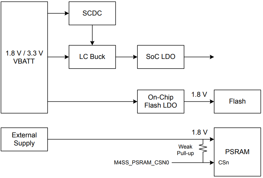
In this configuration, the on-chip LC Buck converter powers the SoC LDO, the on-chip Flash LDO is used as a 1.8 V supply to flash, and an external 1.8 V supply is connected to the PSRAM. Additionally the PSRAM chip select (CSn) has an external weak pull-up resistor to the supply.
Watchdog Timer
The WatchDog Timer is used to generate an interrupt on timeout and a reset in case of system failure which can be caused by an external event like ESD pulse or due to a software failure. Also the Interrupt can be used as a Wakeup source for transitioning from SLEEP/STANDBY to ACTIVE states.
- Independent watchdog timer.
- Interrupt is generated before the system reset is applied which can be used as a wakeup source.
- Generates reset upon Lockup indication from M4 processor.
- Configurable low frequency clock (RC and Xtal).
- Configurable timeout period.
- Able to operate when CPU is in SLEEP state during power-save applications
- Individually controllable power domain for low-power applications.
Calendar
Calendar block acts a RTC with time in seconds, minutes, hours, days, months, years and centuries. The real-time can also be read through APB with accuracy less than a second by reading the millisecond count value and further less also by reading the number of counts of APB clock in 1 millisecond of RTC clock. Accuracy is high.
- Calendar block can provide a seconds trigger and also a msec trigger.
- Calendar block takes care of no. of days in each month and also leap years. It can count up to 4 centuries.
- Real time is readable through APB and also programmable through APB.
General Purpose Timers
The MCU Timer block supports four 32 bit timers, which can be used to generate various timing events for the software. Each of the four timers can be independently programmed to work in periodic or one-shot mode and can be configured either as a microsecond timer or as a counter.
- Four independent 32 bit timers
- Supports per timer enable and disable.
- Option to configure each timer as a 32 bit counter or 32 bit microsecond timer.
- Supports 1 µs mode and 256 µs modes per timer.
- Accounts for integral and fractional value of the time units programmed.
- Microsecond timer supports two modes:
- 1 microsecond mode: The time unit is 1 µs. Number of microseconds required to be counted has to be programmed.
- 256 microsecond mode: The time unit is 256 µs. Number of 256 µs units required to be counted has to be programmed. This is useful when the timer is being used for counting large time values and microsecond based tracking not required.
- One shot and periodic modes per timer.
- Option to interrupt the M4 processor on timeout.
Secure Storage
The Block is used for storing configuration values with data protection feature.
- MCU has 3 set's for storage block
- First chunk is 64 bits
- Second chunk is 64 bits
- Third Chunk is 128 bits
- Each chunk is a power domain.
- Secure mode is available for first and second Chunk.
- Storage space can be used for storing Configuration values
MVP
The Matrix Vector Processor (MVP) offloads floating point operations, particularly matrixed complex floating point multiplies and additions. The MVP was designed to offload the major computations of the Angle-of-Arrival (AoA) MUSIC algorithm, although the architecture can generally be used to offload other heavily floating-point computational problems such as Machine Learning (ML), Eigen, or BLAS acceleration.
Instruction Set Architecture (ISA)
- General purpose instruction set tailored towards algorithms built out of ALU, loop, and load/store instructions
Enables many high-level array functions, e.g.:
- Matrix multiplication
- Element-wise matrix multiplication
- Matrix addition
- Power series generation
- Convolution
Program flexibility allows efficient iteration over N-dimensional array elements, including in-place processing of special matrix views:
- Element-wise negate / conjugate
- Transpose / adjoint / reverse
- Matrix blocks (i.e., rectangular parts of matrix)
- Matrix slices (i.e., taking rows, columns, or elements uniformly spaced within a matrix)
- Row-major or column-major ordering
Arithmetic Logic Unit (ALU)
Support for floating point real and complex numbers
Partial integer input support
- Floating-point output operands, interpreted as 16-bit real or 32-bit complex number (16-bit real and 16-bit imaginary)
- Register bank to hold all input/output operands
- Includes 8 registers for temporary storage and/or accumulation
Hardware to support 1 complex floating point multiply-accumulate (MAC) per cycle
- Four single-precision floating-point multipliers
- Four single-precision floating-point adders
- 6x performance of Cortex M33 FMAC operations
Operations supported at a rate of one operation per cycle:
- Complex addition, multiplication, and MAC operations
- Parallel real multiplication and MAC
- Parallel real addition
- Sum of 4 reals
- Squared-magnitude of complex/real
- Integer-to-float conversion
- Conditional computation
Input transformations (per real/complex part of each input)
- Negation (complex conjugate)
- Zero-masking (real/imaginary part decomposition)
Load/Store Unit (LSU)
- Controls data streaming from memory-to-ALU and vice versa
- Pipelined architecture to support two simultaneous 32-bit memory reads and one 32-bit memory write per cycle
- Supports signed / unsigned 8-bit integer conversion for both load and store operations
First-party DMA ports
- Used by load / store unit for handling accesses to external (system) memory addresses
- Three independent 32-bit AHB manager ports for supporting 2 read channels and 1 write channel simultaneously
Sequencer
- Coordinates all MVP blocks to execute a sequence of instructions provided via the programming interface
- Handles array iteration according to instruction sequence and static array configuration
- Handles loop iteration according to instruction sequence and static loop configuration
Programming interface
- Control registers for starting / stopping engine
Status registers about ongoing and finished instruction sequences
- Fault status
- Useful information for debug
- Breakpoint and stepping controls for debug
Interrupts and faults
- Instruction sequence completion
- Bus faults
- Loop faults
- Array faults
- Array configuration registers
- Loop configuration registers
Instruction queue registers
- Array iteration
- ALU operations
- Looping
SYSRTC
The SYSRTC (System Real Time Clock) is a highly configurable RTC capable of serving multiple cores. It contains up to 2 groups, where the number of capture and compare channels within each group is parametrized individually. Each group has its own interrupt and configuration registers. The main idea is to save power by letting all groups share a single counter.
- 32-bit counter
- 32 kHz / 1 kHz intended operation
- Low energy mode and wake-up
- Up to 2 groups
- 1-2 compare channels per group
- 0-1 capture channel per group
- Optional debug halting
- Optional alternate interrupt/wake-up per group
- Software Reset
Analog Peripherals and Interfaces
Capacitive Touch
- 8 input channels - all the input channels are shared with GPIOs
- 1 shield channel - To reduce sensitivity to mesh capacitance
- Capacitive input and resistor input are connected to two GPIOs each
- Programmable input clock source from the available clocks in the chip
- Controls the rate of scanning for all sensors with configurable inter sensor scan ON time
- Supports both samples streaming and cumulative average mode
- DMA capable
- 8, 16 and 32-bit pseudo-random number for generating two non overlapping streams with configurable delay
- Programmable polynomial and seed values for pseudo-random number generator
- Provides wake up indication after capacitive touch sensing
Analog to Digital Converter (ADC)
The ADC with up to 12 bits of resolution at 2.5 Msps
- 12 bit ADC Output in 2's complement representation
GPIOs in High Power mode for ADC Operation
Signal Ended Mode
- 17 External configuration selection
5 Internal configuration selection
- Internal Temperature sensor
- 3 Opamp Outputs
DAC output for internal reference
- Differential Mode
- 8 external differential mode configuration selection
4 Internal configuration selection.
- 3 Opamp Outputs
- DAC output for internal reference
GPIOs in Low Power mode for ADC Operation
Signal Ended Mode
- 11 External configuration selection.
5 Internal configuration selection.
- Internal Temperature sensor.
- 3 Opamp Outputs
- DAC output for internal reference
Differential Mode
- 5 external differential mode configuration selection.
4 Internal configuration selection.
- 3 Opamp Outputs
- DAC output for internal reference
- 10 MHz to 32 KHz allowed ADC_CLK
- Configurable DMA to support 16 channels for storing AUXADC data in ULP SRAM.
- Measurement range 0 to AUXADC_VREF (1.8 V to 3.3 V)
The ADC has five modes of operation:
- Single ended input with noise averaging
- Single ended input without noise averaging
- Differential input with noise averaging
- Differential input without noise averaging
- Shutdown mode
Digital to Analog Converter (DAC)
DAC can take 10 bit digital inputs and convert them into analog voltage within range 5*vdd/36 to 31*vdd/36. Vdd can vary from 1.8 volts to 3.63 volts.
- 10-bit resolution
- Single ended DAC
- Monotonic by design
- Max sampling frequency is 5 MHz for DAC_CLK
- Supports Operational mode and Shutdown modes
OPAMP
- 3 general purpose Operational Amplifiers (OPAMP) offering rail-to-rail inputs and outputs.
- Each of the three opamps has 2 inputs (inp, inn) and 1 output.
- opamps can take inputs from GPIOs and their outputs can be seen on GPIOs
- configured in either low power mode or high power mode
opamps can be configured as:
- Unity gain amplifier
- Trans-Impedance Amplifier(TIA)
- Non-inverting Programmable Gain Amplifier (PGA)
- Inverting Programmable Gain Amplifier
- Non-inverting Programmable hysteresis comparator
- Inverting Programmable hysteresis comparator
- Cascaded Non-Inverting PGA
- Cascaded Inverting PGA
- Two opamps Differential Amplifier
- Instrumentation Amplifier
Analog Comparators
Analog comparators peripheral consists of two analog comparators, a reference buffer, a scaler and a resistor bank. Both comparators can take inputs from GPIOs.
The comparator compares analog inputs p and n to produce a digital output, cmp_out according to:
p > n, cmp_out = 1
p < n, cmp_out = 0
The following cases of comparison are possible
- Compare external pin inputs
- Compare external pin input to internal voltages.
- Compare internal voltages.
The inputs of 2 comparators can be programmed independently. The reference buffer, scaler and resistor bank are shared between the two comparators and can be enabled only when at least one of the comparators is enabled.
Temperature Sensor
A BJT-based temperature sensor is included on the device.
The BJT based sensor works for a temperature range from -40 °C to 125 °C across the supply range 1.8 V to 3.63 V. It outputs a digital word with a resolution of nearly 1 degree C. The conversion time is 2 clock cycles of ADC after turning ON the temperature sensor.
The temperature reading of the sensor is accessed by configuring the ADC inputs to temperature sensor.
Bootloader
The Bootloader controls the initial operation of the device after any form of reset. The Bootloader supports Flash programming and initial startup of the application code. Bootloader supports following features:
- Two Bootloaders - Security Bootloader and Application Bootloader
- Support for ISP (In-System Programming) through multiple interfaces - UART, SPI and SDIO
- Auto-detection of ISP interface. The host interfaces are the external peripheral interfaces over which Bootloader can receive commands or firmware when in ISP mode. The Bootloader supports UART, SPI and SDIO interfaces. Bootloader in ISP mode waits for data on any of these interfaces and can automatically detect which interface the data is being received.
- Support for secure boot
- Support for secure firmware upgrade using PUF based Roots-of-Trust (RoT)
- Anti-rollback protection. This feature prevents the firmware version from being downgraded. A new firmware is allowed to be upgraded only if it is be equal to or greater than the current firmware.
- Secure Key Management and Protection
- Support for different flash protection levels and write-protected Flash
- Secure XIP from Flash
- Fail-proof migration of current active firmware to new (update) firmware
- Public key cryptography (digital signature) based authentication
The SL917 includes two Bootloaders - Security Bootloader and Application Bootloader. The Security Bootloader runs on the Security processor and the Application Bootloader runs on the Cortex M4 processor. On any reset, execution will always start in Security Bootloader, which is responsible for all security features, ISP and firmware upgrades. Once the Security Bootloader finishes its tasks, it enables the Application Bootloader. The Application bootloader will load and execute the application and also execute wakeup sequence on wakeup from sleep.
The following are the sources, which can trigger the Bootloader:
- Primary reset (RESET_N)
- Power on reset (POC_IN)
- Watchdog reset
- Black out monitor
- Reset request through SYSRESETREQn bit in the Cortex-M4 processor
- Wake-up from Sleep
Security
Security Features
- Secure Boot
- Secure OTA Firmware update
- TRNG: Generates high-entropy random numbers based on RF noise, increasing the effort/time needed to expose secret keys
- Secure Zone
- Secure Key storage : HW device identity and key storage with PUF
- Debug Lock
- Anti Rollback : Firmware downgrade to a lower version is prohibited through OTP to prevent the use of older, potentially vulnerable FW version
- Secure XIP from flash with XTS/CTR mode
- Secure Attestation : Allows a device to authenticate its identity using a cryptographically signed token and exchange of secret keys
- Hardware Accelerators: AES128/256/192, SHA256/384/512, HMAC, RNG, CRC, SHA3, AES-GCM/ CMAC, ChaCha-poly
- Software Implementation: RSA and ECC
- Programmable Secure Hardware Write protect for Flash sectors
Secure Bootup
Key Features
- Ensures your device runs authentic code in the boot and OTA update to eliminate malware insertion threats
- Secure Immutable Bootloader in ROM.
- Authenticates signatures of all other SW using public keys.
- Protocol and Application flash images can be encrypted with separate keys.
On reset, the Security Bootloader configures the module hardware based on the configuration present in the eFuse. It also passes the required information from the eFuse to the Application Bootloader. The Security Bootloader validates the integrity and authenticity of the firmware in the Flash and invokes the Application Bootloader. It detects and prevents execution of unauthorized software during the boot sequence. The Bootloader uses public & private key based digital signatures to recognize authentic software. The Security Boot- loader provides provision for inline execution (XIP) of encrypted firmware from Flash. The Bootloader provides 3 flash protection levels which can be used to secure different sections of the Flash for different purposes:
- Protection level 1: Stored at manufacturing, not allowed to modify by the Security Bootloader
- Protection level 2: Allowed to modify by the Bootloader only, usually used to maintain secure information used/consumed by Boot- loader
- Protection level 3: Allowed to modify by the Bootloader only, usually used to maintain protected firmware images. (Minimum 8 MB of flash is required for complete NWP image protection. For 4 MB flash OPNs, only partial protection is available for NWP image).
The protection levels are written to Flash during the manufacturing process. The write-protection feature prevents the application pro- gram from changing the Flash protection levels.
The Security configurations can be enabled or disabled during the manufacturing process.
Secure XiP
- Execute SW directly from Flash instead of copying it into RAM
- Images are saved in encrypted format and decrypted using device-specific PUF intrinsic keys while executing. In-line decryption based on-the-fly AES engine (based on PUF keys). Multiple protection levels can be set for flash, including unmodifiable. XTS/CTR modes supported.
Secure Firmware Upgrade
Secure firmware upgrade via host interface :
The secure firmware upgrade feature of the Bootloader checks the authenticity of the new firmware image along with its integrity. The Bootloader automatically detects the host interface in use and configures the host interface hardware accordingly. The Bootloader up- dates the image only after successfully validating the authenticity and integrity of the image. It prevents downgrade to a lower version of firmware using the anti-rollback feature, if it is enabled. The Bootloader also supports transparent migration to a wirelessly updated im- age and protection against failures by providing recovery mechanisms.
Secure OTA :
- Secure OTA update to eliminate malware insertion threats.
- Wireless and Application image transfer over the air.
- Wireless processor authenticates the signatures of OTA image using public keys
- Bootloader copies the OTA image to primary firmware location upon successful authentication .
Secure Zone
Key Features
- Barrier between the Security/Protocol core and Application core.
- No access to the security processor, memory, and HW registers from external peripherals, including the Cortex-M4
The Secure Zone is hardware enforced isolation between the trusted and non-trusted blocks in the system. Secure zone protects the secure assets residing in secure execution environment by restricting direct access. It also provides a secure execution environment to store confidential data. The Bootloader configures Secure Zone, secure firmware upgrade and secure bootup in "Secure Zone enabled" mode. This mode is programmed during the manufacturing process.
In-System Programming (ISP)
In System Programming (ISP) is programming or reprogramming of the flash through boot loader using UART (GPIO_8, GPIO_9), SPI (GPIO_25 to GPIO_28), and SDIO (GPIO-25 to GPIO-30) interfaces. This can be done after the part is integrated on end-user board. Boot loader can be requested to boot in ISP mode by pulling down a specific GPIO pin. This pin has to be left unconnected during reset for the boot loader to bypass ISP and execute the code that is present in flash. ISP mode can be used to reprogram the flash, if the application codes use JTAG pins for functional use. On boot up, if the application code goes into a state where JTAG interface is not functioning, ISP mode can be used to gain the control and to reprogram the flash.
Debug Lock
Key Features
- Debug ports are disabled in HW by default.
- It can be enabled in SW using cryptographically secure host interface commands validated by immutable bootloader
- It allows the device's JTAG ports to be locked and unlocked.
Debug Support
MCU implements complete hardware debug solution. This provides high system visibility of the M4 processor and memory through either a traditional JTAG port or a 2-pin Serial Wire Debug (SWD) port that is ideal for microcontrollers and other small package devices.
In Serial Wire Viewer (SWV) mode, a one-bit serial protocol is used and this reduces the number of output signal to one. When combining SWV with Serial-Wire debug protocol, the Text Data Output (TDO) pin normally used for Joint Test Action Group (JTAG) protocol can be shared with SWV.
The Embedded Trace Macrocell (ETM) provides high bandwidth instruction trace via four dedicated trace. The MCU_CLK_OUT frequency must be in the range of 40 MHz to 90 MHz to Instruction trace using ETM component.
WLAN
- Compliant to single-spatial stream IEEE 802.11 b/g/n/ax with single band (2.4 GHz) support
- Support for 20 MHz channel bandwidth for 802.11n and 802.11ax.
- Operating Modes: Wi-Fi 4 STA, Wi-Fi 6 (802.11ax) STA, Wi-Fi 4 AP, Enterprise STA, Wi-Fi 6 STA + Wi-Fi 4 AP, Wi-Fi STA + BLE
- Wi-Fi 6 Features: Individual Target wake-up time (iTWT), Broadcast TWT (bTWT),SU extended range (ER), DCM (Dual Carrier Modulation), DL MU-MIMO, DL/UL OFDMA, MBSSID, BFRP, Spatial Re-use, BSS Coloring, and NDP feedback up to 4 antennas
- Integrated PA
- Data Rates—802.11b: up to 11 Mbps; 802.11g: up to 54 Mbps; 802.11n: MCS0 to MCS7; 802.11ax: MCS0 to MCS7
- Operating Frequency Range [MHz]: 2412-2462 (North America, default), 2412-2472 (Europe, and other countries where applicable), 2412-2484 (Japan)
MAC
- Conforms to IEEE 802.11b/g/n/j/ax standards for MAC
- Hardware accelerators for AES
- WPA, WPA2, WPA3 and WMM support
- AMPDU aggregation for high performance
- Firmware downloaded from host based on application
- Hardware accelerators for DH (for WPS) and ECDH
Baseband Processing
- Supports 11b: DSSS for 1, 2 Mbps and CCK for 5.5, 11 Mbps
Supports all OFDM data rates
- 802.11g: 6, 9, 12, 18, 24, 36, 48, 54 Mbps
- 802.11ax, 802.11n: MCS 0 to MCS 7
- High-performance multipath handling in OFDM, DSSS, and CCK modes
Bluetooth
Key Features
- Transmit power up to +17 dBm with integrated PA
- Receive sensitivity — LE: -93 dBm, LR 125 Kbps: -104.5 dBm
- Operating Frequency Range — 2.402 GHz - 2.480 GHz
- Supports Bluetooth® Low Energy (LE): High Speed (1Mbps and 2Mbps) and Long Range (LE Coded PHYs, 125Kbps and 500Kbps; these are referred to as "LR" throughout this data sheet)
- Advertising extensions
- Data length extensions
- LL privacy
- LE dual role
- BLE acceptlist
- Two simultaneous BLE connections (2 peripheral or 2 central, or 1 central and 1 peripheral)
- BLE Mesh (4 nodes) for limited switch use case.
MAC
Link Manager
- Creation, modification & release of physical links
- Connection establishment between Link managers of two Bluetooth devices
- Link supervision is implemented in Link Manager
- Link power control is done depending on the inputs from Link Controller
- Enabling & disabling of encryption & decryption on logical links
- AES hardware acceleration
Link Controller
- Encodes and decodes header of BLE packets
- Manages flow control, acknowledgment, re-transmission requests, etc.
- Stores the last packet status for all physical transports
- Indicates the success status of packet transmission to upper layers
- Indicates the link quality to the LMP layer
Device Manager
- Executes HCI Commands
- Controls Scan & Connection processes
- Controls all BLE Device operations except data transport operations
- BLE Controller state transition management
- Anchor point synchronization & management
- Scheduler
Baseband Processing
Supports BLE 1 Mbps, 2 Mbps and long range 125 kbps, 500 kbps
RF Transceiver
- The SL917 features two highly configurable RF transceivers supporting WLAN 11b/g/n/ax and Bluetooth LE wireless protocols. Both RF transceivers together operating in multiple modes covering High Performance (HP) and Low Power (LP) operations. List of operating modes are given in next section.
- It contains two fully integrated fractional-N frequency synthesizers having reference from internal oscillator with 40 MHz crystal. One of the synthesizer is a low power architecture which also caters single-bit data modulation feature for Bluetooth LE protocols.
Receiver and Transmitter Operating Modes
The available radio operating modes are
- WLAN HP TX - WLAN High-Performance Transmitter
- WLAN HP RX - WLAN High-Performance Receiver
- WLAN LP RX - WLAN Low-Power Receiver
- BLE HP TX - Bluetooth LE High-Performance Transmitter
- BLE HP RX - Bluetooth LE High-Performance Receiver
- BLE LP TX - Bluetooth LE Low-Power Transmitter
- BLE LP RX - Bluetooth LE Low-Power Receiver
Note: All the TX / RX modes are automatically controlled by radio firmware and not individually selectable.
Embedded Wi-Fi Software
- The wireless software package supports Embedded Wi-Fi (802.11 b/g/n/ax) Client mode, Wi-Fi Access point mode (up to 4 clients), and Enterprise Security in client mode.
- The software package includes complete firmware and application profiles.
- It has a wireless coexistence manager to arbitrate between protocols.
Security
Wireless software supports multiple levels of security capabilities available for the development of IoT devices.
- Accelerators: AES128/256
- WPA/WPA2/WPA3-Personal, WPA/WPA2 Enterprise for Client
Low Power Modes
It supports Ultra-low power consumption with multiple power modes to reduce system energy consumption.
- Voltage and Frequency Scaling
- Deep sleep (ULP) mode with only the sleep timer active – with and without RAM retention
- Wi-Fi standby associated mode with automatic periodic wake-up
- Automatic clock gating of the unused blocks or transit the system from Normal to ULP mode.
ULP Mode
In Ultra Low Power mode, the deep sleep manager has control over the other subsystems and M4 processors and controls their active and sleep states. During deep sleep, the always-on logic domain operates on a lowered supply and a low-frequency clock to reduce power consumption. The ULP mode supports the following wake-up options:
- Timeout wakeup - Exit sleep state after programmed timeout value.
- GPIO Based Wakeup: Exit sleep state when GPIO goes High/Low based on programmed polarity.
- Analog Comparator Based wakeup - Exit sleep state on an event at the analog comparator.
- RTC Timer wakeup - Exit Sleep state on timeout of RTC timer
- WatchDog Interrupt based wakeup - Exit Sleep state upon watchdog interrupt timeout.
Wireless Subsystem Memory
On-Chip Memory
The Network Wireless Processor has the following memory:
- On-chip SRAM of 672/480/416/352 KB based on chip configuration
- 448 KB of ROM which holds the Secure primary bootloader, Network Stack, Wireless stacks and security functions
- 16 KB of Instruction cache enabling eXecute In Place (XIP) with quad SPI flash memory.
- eFuse of 1024 bytes (used to store primary boot configuration, security and calibration parameters) The Following memory configuration between MCU and Wireless Sub-system are possible:
| No. | MCU memory size | Wireless Subsystem memory size | Note |
|---|---|---|---|
| 320 KB | 352 KB | PS4 and PS2 power states possible | |
| 256 KB | 416 KB | Only PS4 power state possible For MCU RAM retention, MCU needs to retain complete 320 KB | |
| 192 KB | 480 KB | Only PS4 power state possible For MCU RAM retention, MCU needs to retain complete 320 KB |
Pad Configuration
There are multiple processor sub-systems containing SZP (Secure Zone Processor), MCU HP (High Performance) and MCU ULP (Ultra Low Power) which share these common set of GPIO pads. These GPIO pads are controllable by either SZP, MCU HP or MCU ULP. PAD selection register has to be programmed to control the PAD behavior for each GPIO. The SZP and MCU HPGPIOs are available only in PS4/PS3 power states whereas MCU ULP GPIOs are available in all the power states except sleep modes. The UULP Vbat GPIOs are available in all power states.
The SZP, MCU HP and MCU ULP GPIOs PAD are programmable, multi-voltage (1.8 V, 3.3 V) general purpose, bi-directional I/O buffer with a selectable LVCMOS (Low Voltage CMOS) input or LVCMOS Schmitt trigger input and programmable pull-up/pull-down. In the full-drive mode, this buffer can operate in excess of 100 MHz frequency with 15 pF external load and 125 MHz with 10pF load, but actual frequency is load and system dependent. A maximum of 200 MHz can be achieved under small capacitive loads.
The following PAD configurations can be controlled by software for SZP, MCU HP and MCU ULP GPIOs.
- Bi-directional IO capability
- Multi-voltage DVDD capability (1.8 V, 3.3 V)
- Power-on-Start (POS) capable
- Optimized for EMC (low di/dt switching supply noise) with SSO (Simultaneous Switching Output) factor of 8
- Four (4) Programmable output drive strengths (rated 2 mA, 4 mA, 8mA, and 12 mA)
- Selectable output slew-rate (slow / fast)
- Open drain output mode (Logic low or high on input and use OEN as data input)
- LVCMOS/LVTTL compatible input with selectable hysteresis
- Programmable input options (pull-up, pull-down, repeater, or plain input)
- No power sequence requirements, I/Os are tri-stated when core power is not valid (POC control). These are tri-stated even if the system is under reset or in the deep sleep power state.
The following PAD configurations can be controlled by software for UULP Vbat GPIOs.
- Bi-directional IO capability
- Multi-voltage DVDD capability (1.8 V, 3.3 V)
Interrupts
- Nested vectored interrupt controller (NVIC) for interrupts handling
- Supports 99 interrupts
- Flexible exception and interrupt management
- Nested exception/interrupt support
- Vectored exception/interrupt entry
- Interrupt configurations, prioritization, and interrupt masking
Hardware Architecture
Block Diagrams
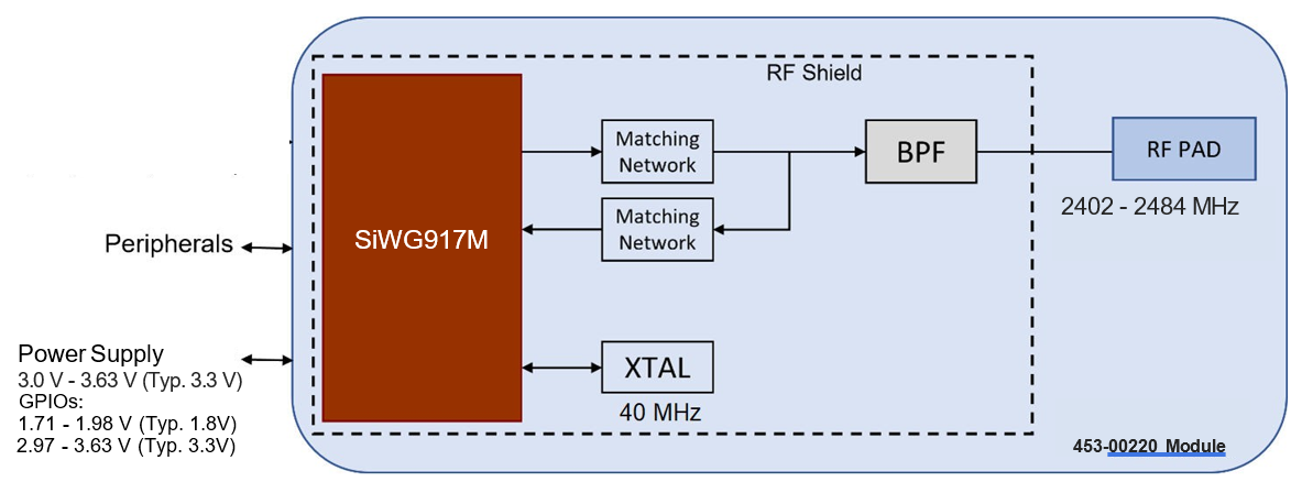
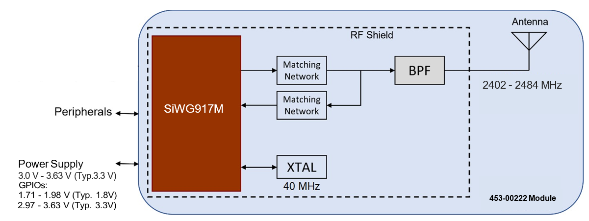
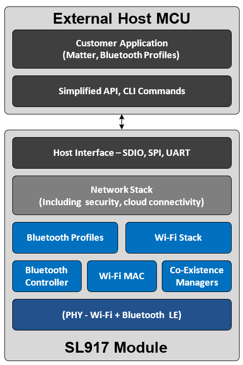
Pin-Out
List of IC Pins Not Available in the Modules
| Pin Name | QFN I/O Supply Domain | Direction | Initial State (Power up, Active Reset) | Description |
|---|---|---|---|---|
| RF_BLETX | RF_AVDD | Output | NA | BLE 8 dBm RF Output |
| ULP_GPIO_10 | ULP_IO_VDD | Inout | HighZ | Default: HighZ Sleep: HighZ Refer to GPIO Pin Multiplexing for configuration |
| XTAL_32KHZ_P | NA | Inout | NA | Analog Pin. 32KHZ XTAL Connection |
| XTAL_32KHZ_N | NA | Inout | NA | Analog Pin. 32KHZ XTAL Connection |
| UULP_VBAT_GPIO_1 | VBATT | Inout | HighZ | Default: High Sleep: High Refer to GPIO Pin Multiplexing for configuration |
| TRST | VBATT | Input | HighZ | Test signal |
Chip Packages - RF and Control Interfaces
| Pin Name | Pin No. | I/O Supply Domain | Direction | Initial State (Power up Active Reset) | Description |
|---|---|---|---|---|---|
| ANT_TUNE_1 | 1 | N/A | Input | N/A | 453-00222: External fine-tuning option for the integral antenna; connect same tun- ing circuit on both ANT_TUNE1 and ANT_TUNE2 pins; leave floating if no fine- tuning is desired on the integral antenna; 453-00220: leave this pin floating |
| RF | 10 | VBATT | Inout | N/A | Connect to antenna with a 50-Ω impedance as per the reference schematics |
| POC_IN | 31 | VBATT | Input | NA | This is an input to the chip which resets all analog and digital blocks in the device. It should be made high only after supplies are valid. |
| POC_OUT | 32 | VBATT | Output | NA | This is internally generated. Initially, it is low. But it becomes high when the supply (VBATT) is valid. |
| RESET_N | 33 | VBATT | Inout | NA | Active-low reset asynchronous reset signal, which resets only digital blocks. RESET_N will be pulled low if POC_IN is low. |
| ANT_TUNE_2 | 61 | N/A | Input | N/A | 453-00222: External fine-tuning option for the integral antenna; connect same tuning circuit on both ANT_TUNE1 and ANT_TUNE2 pins; leave floating if no fine- tuning is desired on the integral antenna; 453-00220: leave this pin floating |
Chip Packages - Power and Ground Pins
| Pin Name | Pin No. | Type | Direction | Description |
| ULP_IO_VDD | 26 | Power | Input | I/O supply for ULP I/Os. Refer to the GPIOs section for details on which GPIOs have this as the I/O supply. |
| VBATT | 34 | Power | Input | Power supply for the module. |
| 1V8_LDO | 36 | Power | Output | Output of 1.8V LDO which is used for Flash sup- ply. |
| IOVDD | 50 | Power | Input | I/O Supply for I/Os. Refer to GPIO Pin Multiplexing for details on which GPIOs have this as the I/O supply. |
| SDIO_IO_VDD | 52 | Power | Input | I/O Supply for SDIO I/Os. Refer to GPIO Pin Multiplexing for details on which GPIOs have this as the I/O supply. |
| FLASH_IO_VDD | 54 | Power | Input | I/O Supply for IC stacked Flash. Connect to 1V8_LDO as per Reference Schematics. |
| GND | 2, 3, 9, 11, 57, 60, 62-71 | Ground | Common ground pins. |
Chip Packages - Peripheral Interfaces
| Pin Name | Pin No. | I/O Supply Domain | Direction | Initial State (Power up Active Reset) | Description |
|---|---|---|---|---|---|
| UULP_VBAT_GPIO_0 | 4 | VBATT | Output | High | Default: High Sleep: High Refer to GPIO Pin Multiplexing for configuration |
| ULP_GPIO_11 | 5 | ULP_IO_VDD | Inout | HighZ | Default: HighZ Sleep: HighZ Refer to GPIO Pin Multiplexing for configuration |
| ULP_GPIO_5 | 6 | ULP_IO_VDD | Inout | HighZ | Default: HighZ Sleep: HighZ Refer to GPIO Pin Multiplexing for configuration |
| ULP_GPIO_7 | 7 | ULP_IO_VDD | Inout | HighZ | Default: HighZ Sleep: HighZ Refer to GPIO Pin Multiplexing Note for configuration |
| ULP_GPIO_4 | 8 | ULP_IO_VDD | Inout | HighZ | Default: HighZ Sleep: HighZ Refer to GPIO Pin Multiplexing for configuration |
| GPIO_55 | 12 | IO_VDD | Inout | HighZ | Default: HighZ Sleep: HighZ Refer toGPIO Pin Multiplexing for configuration |
| JTAG_TMS_SWDIO | 13 | IO_VDD | Input | Pullup | JTAG interface Test Mode Select signal. Bi-directional data pin for SWD interface. |
| JTAG_TDO_SWO | 14 | IO_VDD | Output | Pullup | JTAG interface output data. Serial wire out- put for SWD Interface. This pin can also be used as ISP_ENABLE. Pull down to enable ISP mode. In System Programming (ISP) is programming or reprogramming of the flash through boot loader using UART (GPIO_8,GPIO_9), SPI (GPIO_25 to GPIO_28) and SDIO (GPIO_25 to GPIO_30) interfaces. This can be done after the part is integrated on end user board. Boot loader can be requested to boot in ISP mode by pulling down JTAG_TDO_SWO pin. This pin has to be left unconnected during reset for the boot loader to bypass ISP and execute the code that is present in flash. ISP mode can be used to reprogram the flash, if the application codes uses JTAG pins for other multiplexed functionalities. On boot up, if the ap- plication code goes into a state where JTAG interface is not functioning, ISP mode can be used to gain the control and to reprogram the flash. |
| JTAG_TCK_SWCLK | 15 | IO_VDD | Input | Pullup | JTAG interface clock or serial wire clock |
| JTAG_TDI | 16 | IO_VDD | Input | Pullup | JTAG interface input data |
| GPIO_56 | 17 | IO_VDD | Inout | HighZ | Default: HighZ Sleep: HighZ Refer to GPIO Pin Multiplexing for configuration |
| GPIO_53 | 18 | IO_VDD | Inout | HighZ | Default: HighZ Sleep: HighZ Refer to GPIO Pin Multiplexing for configuration |
| GPIO_54 | 19 | IO_VDD | Inout | HighZ | Default: HighZ Sleep: HighZ Refer to GPIO Pin Multiplexing for configuration |
| GPIO_8/ISP_UART_RX | 20 | IO_VDD | Inout | HighZ | Default: HighZ Sleep: HighZ ISP: UART_RX If ISP is not enabled, refer to GPIO Pin Multiplexing for configuration |
| GPIO_57 | 21 | IO_VDD | Inout | HighZ | Default: HighZ Sleep: HighZ Refer to GPIO Pin Multiplexing for configuration |
| GPIO_9/ISP_UART_TX | 22 | IO_VDD | Inout | HighZ | Default: HighZ Sleep: HighZ ISP: UART_TX If ISP is not enabled, refer to GPIO Pin Multiplexing for configuration |
| ULP_GPIO_6 | 23 | ULP_IO_VDD | Inout | HighZ | Default: HighZ Sleep: HighZ PTA_PRIO: "PTA Priority" input signal is part of 3-wire coexistence (Packet Traffic Arbitration) interface. If PTA feature is ena- bled, use it as PTA_PRIO. If PTA feature is not enabled, refer to GPIO Pin Multiplexing for configuration |
| GPIO_6 | 24 | IO_VDD | Inout | HighZ | Default: HighZ Sleep: HighZ Refer to GPIO Pin Multiplexing for configuration |
| GPIO_52 | 25 | IO_VDD | Inout | HighZ | Default: HighZ Sleep: HighZ Refer to GPIO Pin Multiplexing for configuration |
| ULP_GPIO_9 | 27 | ULP_IO_VDD | Inout | HighZ | Default: HighZ Sleep: HighZ Refer to GPIO Pin Multiplexing for configuration |
| ULP_GPIO_1 | 28 | ULP_IO_VDD | Inout | HighZ | Default: HighZ Sleep: HighZ PTA_REQ: "PTA Request" input signal is part of 3-wire coexistence (Packet Traffic Arbitration) interface. If PTA feature is ena- bled, use it as PTA_REQ. If PTA feature is not enabled, refer to GPIO Pin Multiplexing for configuration |
| UULP_VBAT_GPIO_3 | 29 | VBATT | Inout | HighZ | Default: HighZ Sleep: HighZ Refer to GPIO Pin Multiplexing for configuration |
| UULP_VBAT_GPIO_2 | 30 | VBATT | Inout | HighZ | Default: HighZ Sleep: HighZ Refer to GPIO Pin Multiplexing for configuration |
| ULP_GPIO_0 | 35 | ULP_IO_VDD | Inout | HighZ | Default: HighZ Sleep: HighZ Refer to GPIO Pin Multiplexing for configuration |
| ULP_GPIO_8 | 37 | ULP_IO_VDD | Inout | HighZ | Default: HighZ Sleep: HighZ Refer to GPIO Pin Multiplexing for configuration |
| GPIO_7 | 38 | IO_VDD | Inout | HighZ | Default: HighZ Sleep: HighZ PTA_GRANT: "PTA Grant" output signal is part of 3-wire coexistence (Packet Traffic Arbitration) interface. If PTA feature is enabled, use it as PTA_GRANT. If PTA feature is not enabled, refer to GPIO Pin Multiplexing for configuration. |
| GPIO_48 | 39 | IO_VDD | Inout | HighZ | Default: HighZ Sleep: HighZ Refer to GPIO Pin Multiplexing for configuration |
| GPIO_47 | 40 | IO_VDD | Inout | HighZ | Default: HighZ Sleep: HighZ Refer to GPIO Pin Multiplexing for configuration |
| GPIO_49 | 41 | IO_VDD | Inout | HighZ | Default: HighZ Sleep: HighZ Refer to GPIO Pin Multiplexing for configuration |
| GPIO_50 | 42 | IO_VDD | Inout | HighZ | Default: HighZ Sleep: HighZ Refer to GPIO Pin Multiplexing for configuration |
| GPIO_51 | 43 | IO_VDD | Inout | HighZ | Default: HighZ Sleep: HighZ Refer to GPIO Pin Multiplexing for configuration |
| GPIO_46 | 44 | IO_VDD | Inout | HighZ | Default: HighZ Sleep: HighZ Refer to GPIO Pin Multiplexing for configuration |
| GPIO_30/SDIO_D3 | 45 | SDIO_IO_VDD | Inout | Pullup | Default: HighZ Sleep: HighZ ISP: SDIO_D3 If ISP is not enabled, refer to GPIO Pin Multiplexing for configuration |
| GPIO_27/SDIO_D0/ HSPI_MOSI | 46 | SDIO_IO_VDD | Inout | HighZ | Default: HighZ Sleep: HighZ ISP: SDIO_DO or HSPI_MOSI If ISP is not enabled, refer to GPIO Pin Multiplexing for configuration |
| GPIO_29/SDIO_D2/ HSPI_INTR | 47 | SDIO_IO_VDD | Inout | HighZ | Default: HighZ Sleep: HighZ ISP: SDIO_D2 or HSPI_MISO If ISP is not enabled, refer to GPIO Pin Multiplexing for configuration |
| GPIO_28/SDIO_D1/ HSPI_MISO | 48 | SDIO_IO_VDD | Inout | HighZ | Default: HighZ Sleep: HighZ ISP: SDIO_D1 or HSPI_MISO If ISP is not enable, refer to GPIO Pin Multiplexing for configuration |
| GPIO_25/SDIO_CLK/ HSPI_CLK | 49 | SDIO_IO_VDD | Inout | HighZ | Default: HighZ Sleep: HighZ ISP: SDIO_CLK or HSPI_CLK If ISP is not enabled, refer to GPIO Pin Multiplexing for configuration |
| ULP_GPIO_2 | 51 | ULP_IO_VDD | Input | HighZ | Default: HighZ Sleep: HighZ Refer to GPIO Pin Multiplexing for configuration |
| GPIO_26/SDIO_CMD/ HSPI_CSN | 53 | SDIO_IO_VDD | Inout | HighZ | Default: HighZ Sleep: HighZ ISP: SDIO_CMD or HSPI_CSN If ISP is not enabled, refer to GPIO Pin Multiplexing for configuration |
| GPIO_10 | 55 | IO_VDD | Inout | HighZ | Default: HighZ Sleep: HighZ Refer to GPIO Pin Multiplexing for configuration |
| GPIO_12 | 56 | IO_VDD | Inout | HighZ | Default: HighZ Sleep: HighZ Refer to GPIO Pin Multiplexing for configuration |
| GPIO_11 | 58 | IO_VDD | Inout | HighZ | Default: HighZ Sleep: HighZ Refer to GPIO Pin Multiplexing for configuration |
| GPIO_15 | 59 | IO_VDD | Inout | HighZ | Default: HighZ Sleep: HighZ Refer to GPIO Pin Multiplexing for configuration |
GPIO Pin Multiplexing
Note:
- SL917 has the support for 45 GPIOs. These GPIOs are grouped into SoC GPIOs, ULP GPIOs, and UULP GPIOs.
- The possible GPIO combinations for each Peripheral Interface are listed in Section 6.4 Valid GPIO Sets for Peripherals.
- The digital GPIOs SOCPERH_ON_ULP_GPIO_0 to SOCPERH_ON_ULP_GPIO_11 are mapped onto physical ULP GPIOs for SoC Peripheral functionality and digital GPIOs LPPERH_ON_SOC_GPIO_0 to ULPPERH_ON_SOC_GPIO_11 are mapped onto physical SoC GPIOs for ULP Peripheral functionality. Refer to Section 6.3.5 Digital Functions for peripheral mapping on these GPIOs
SoC GPIO Pin Multiplexing
The SoC GPIOs shown below (GPIO_6 to GPIO_57) are available in the normal mode of operation (Power-states 4 and 3). Default mode is mode0 (Mode = 0) if not explicitly mentioned. For a description of power-states, refer to the Power States section of the Reference Manual. Each of these GPIOs Pin function is controlled by the GPIO Mode register mentioned in SoC GPIOs section of the Reference Manual.
| GPIO | GPIO Modes 0, 1, 2, 3, 4, 5 | GPIO Modes 6, 7, 8, 9, 10, 11 | GPIO Modes 12, 13, 14, 15 |
|---|---|---|---|
| GPIO_6 | 0: GPIO_6 | 6: UART1_RX | 12: GSPI_MOSI |
| 1: | 7: I2S0_DIN_1 | 13: M4SS_TRACE_CLKIN | |
| 2: USART0_CTS | 8: PMU_TEST_1 | 14: | |
| 3: SSI_MST_DATA2 | 9: ULPPERH_ON_SOC_GPIO_0 | 15: NWP_GPIO_6 | |
| 4: I2C0_SDA | 10: PWM_0L | ||
| 5: I2C1_SCL | 11: M4SS_QSPI_D0 | ||
| GPIO_7 | 0: GPIO_7 | 6: UART1_TX | 12: M4SS_QSPI_CSN1 |
| 1: | 7: I2S0_DOUT_1 | 13: M4SS_TRACE_CLK | |
| 2: USART0_DTR | 8: PMU_TEST_2 | 14: | |
| 3: SSI_MST_DATA3 | 9: ULPPERH_ON_SOC_GPIO_1 | 15: | |
| 4: I2C0_SCL | 10: PWM_0H | ||
| 5: I2C1_SDA | 11: M4SS_QSPI_CSN0 | ||
| GPIO_8 / ISP_UART_RX | 0: GPIO_8 | 6: UART1_RS485_RE | 12: |
| 1: | 7: I2S0_CLK | 13: M4SS_TRACE_D0 | |
| 2: USART0_CLK | 8: SSI_SLV_CLK | 14: | |
| 3: SSI_MST_CLK | 9: ULPPERH_ON_SOC_GPIO_2 | 15: NWP_GPIO_8 | |
| 4: GSPI_CLK | 10: PWM_1L | ||
| 5: QEI_IDX | 11: M4SS_QSPI_CLK | ||
| GPIO_9 / ISP_UART_TX | 0: GPIO_9 | 6: UART1_RS485_DE | 12: |
| 1: | 7: I2S0_WS | 13: M4SS_TRACE_D1 | |
| 2: USART0_RTS | 8: SSI_SLV_CS | 14: | |
| 3: SSI_MST_CS0 | 9: ULPPERH_ON_SOC_GPIO_3 | 15: NWP_GPIO_9 | |
| 4: GSPI_CS0 | 10: PWM_1H | ||
| 5: QEI_PHA | 11: M4SS_QSPI_D1 | ||
| GPIO_10 | 0: GPIO_10 | 6: UART1_RTS | 12: SSI_MST_DATA1 |
| 1: | 7: I2S0_DIN_0 | 13: M4SS_TRACE_D2 | |
| 2: USART0_RX | 8: SSI_SLV_MOSI | 14: | |
| 3: SSI_MST_CS1 | 9: ULPPERH_ON_SOC_GPIO_4 | 15: NWP_GPIO_10 | |
| 4: GSPI_CS1 | 10: PWM_2L | ||
| 5: QEI_PHB | 11: M4SS_QSPI_D2 | ||
| GPIO_11 | 0: GPIO_11 | 6: UART1_CTS | 12: MCU_CLK_OUT |
| 1: | 7: I2S0_DOUT_0 | 13: M4SS_TRACE_D3 | |
| 2: USART0_DSR | 8: SSI_SLV_MISO | 14: | |
| 3: SSI_MST_DATA0 | 9: ULPPERH_ON_SOC_GPIO_5 | 15: NWP_GPIO_11 | |
| 4: GSPI_MISO | 10: PWM_2H | ||
| 5: QEI_DIR | 11: M4SS_QSPI_D3 | ||
| GPIO_12 | 0: GPIO_12 | 6: UART1_RS485_EN | 12: |
| 1: | 7: | 13: | |
| 2: USART0_DCD | 8: MCU_CLK_OUT | 14: | |
| 3: SSI_MST_DATA1 | 9: ULPPERH_ON_SOC_GPIO_6 | 15: NWP_GPIO_12 | |
| 4: GSPI_MOSI | 10: PWM_3L | ||
| 5: | 11: | ||
| GPIO_15 | 0: GPIO_15 | 6: M4SS_TRACE_CLKIN | 12: |
| 1: | 7: | 13: | |
| 2: USART0_TX | 8: MCU_CLK_OUT | 14: | |
| 3: SSI_MST_CS2 | 9: ULPPERH_ON_SOC_GPIO_7 | 15: NWP_GPIO_15 | |
| 4: GSPI_CS2 | 10: PWM_3H | ||
| 5: | 11: | ||
| GPIO_25 / SDIO_CLK / HSPI_CLK | 0: GPIO_25 1: | 6: 7: I2S0_CLK | 12: SOC_PLL_CLOCK 13: USART0_IR_RX |
| 2: USART0_CLK | 8: SSI_SLV_CS | 14: TopGPIO_0 | |
| 3: SSI_MST_CLK | 9: SCT_IN_0 | 15: | |
| 4: GSPI_CLK | 10: PWM_FAULTA | ||
| 5: QEI_IDX | 11: ULPPERH_ON_SOC_GPIO_6 | ||
| GPIO_26 / SDIO_CMD / HSPI_CSN | 0: GPIO_26 1: | 6: UART1_RS485_EN 7: I2S0_WS | 12: INTERFACE_PLL_CLOCK 13: USART0_IR_TX |
| 2: USART0_CTS | 8: SSI_SLV_CLK | 14: TopGPIO_1 | |
| 3: SSI_MST_DATA0 | 9: | 15: | |
| 4: GSPI_MISO | 10: PWM_FAULTB | ||
| 5: QEI_PHA | 11: ULPPERH_ON_SOC_GPIO_7 | ||
| GPIO_27 / SDIO_D0 / HSPI_MOSI | 0: GPIO_27 1: | 6: UART1_RTS 7: I2S0_DIN_0 | 12: I2S_PLL_CLOCK 13: USART0_RS485_EN |
| 2: USART0_RI | 8: SSI_SLV_MOSI | 14: TopGPIO_2 | |
| 3: SSI_MST_DATA1 | 9: | 15: | |
| 4: GSPI_MOSI | 10: PWM_TMR_EXT_TRIG_1 | ||
| 5: QEI_PHB | 11: ULPPERH_ON_SOC_GPIO_8 | ||
| GPIO_28 / SDIO_D1 / HSPI_MISO | 0: GPIO_28 1: | 6: UART1_CTS 7: I2S0_DOUT_0 | 12: XTAL_ON_IN 13: USART0_RS485_RE |
| 2: USART0_RTS | 8: SSI_SLV_MISO | 14: TopGPIO_3 | |
| 3: SSI_MST_CS0 | 9: | 15: | |
| 4: GSPI_CS0 | 10: PWM_TMR_EXT_TRIG_2 | ||
| 5: QEI_DIR | 11: ULPPERH_ON_SOC_GPIO_9 | ||
| GPIO_29 / SDIO_D2 / HSPI_INTR | 0: GPIO_29 1: | 6: UART1_RX 7: I2S0_DIN_1 | 12: USART0_DCD 13: USART0_RS485_DE |
| 2: USART0_RX | 8: PMU_TEST_1 | 14: TopGPIO_4 | |
| 3: SSI_MST_DATA2 | 9: SCT_OUT_0 | 15: | |
| 4: GSPI_CS1 | 10: PWM_TMR_EXT_TRIG_3 | ||
| 5: I2C1_SCL | 11: ULPPERH_ON_SOC_GPIO_10 | ||
| GPIO_30 / SDIO_D3 | 0: GPIO_30 | 6: UART1_TX | 12: PMU_TEST_1 |
| 1: | 7: I2S0_DOUT_1 | 13: PMU_TEST_2 | |
| 2: USART0_TX | 8: PMU_TEST_2 | 14: TopGPIO_5 | |
| 3: SSI_MST_DATA3 | 9: SCT_OUT_1 | 15: | |
| 4: GSPI_CS2 | 10: PWM_TMR_EXT_TRIG_4 | ||
| 5: I2C1_SDA | 11: ULPPERH_ON_SOC_GPIO_11 | ||
| JTAG_TCK_SWCLK | 0: GPIO_31 | 6: | 12: UART1_RTS |
| 1: | 7: | 13: QEI_IDX | |
| 2: | 8: | 14: | |
| 3: | 9: | 15: | |
| 4: | 10: | ||
| 5: | 11: I2C0_SDA | ||
| JTAG_TDI | 0: GPIO_32 | 6: | 12: UART1_CTS |
| 1: | 7: | 13: QEI_PHA | |
| 2: | 8: | 14: | |
| 3: | 9: | 15: | |
| 4: | 10: | ||
| 5: | 11: I2C0_SCL | ||
| JTAG_TMS_SWDIO | 0: GPIO_33 | 6: | 12: UART1_RX |
| 1: | 7: | 13: QEI_PHB | |
| 2: | 8: | 14: | |
| 3: | 9: | 15: | |
| 4: | 10: | ||
| 5: | 11: I2C1_SCL | ||
| JTAG_TDO_SWO | 0: GPIO_34 | 6: | 12: UART1_TX |
| 1: | 7: | 13: QEI_DIR | |
| 2: | 8: | 14: | |
| 3: | 9: | 15: | |
| 4: | 10: | ||
| 5: | 11: I2C1_SDA | ||
| GPIO_46 | 0: GPIO_46 | 6: M4SS_TRACE_CLKIN | 12: |
| 1: M4SS_QSPI_CLK | 7: I2S0_CLK | 13: | |
| 2: USART0_RI | 8: SSI_SLV_CS | 14: | |
| 3: QEI_IDX | 9: ULPPERH_ON_SOC_GPIO_8 | 15: NWP_GPIO_46 | |
| 4: GSPI_CLK | 10: SOC_PLL_CLOCK | ||
| 5: | 11: M4SS_PSRAM_CLK | ||
| GPIO_47 | 0: GPIO_47 | 6: M4SS_TRACE_CLK | 12: |
| 1: M4SS_QSPI_D0 | 7: I2S0_WS | 13: | |
| 2: USART0_IR_RX | 8: SSI_SLV_CLK | 14: | |
| 3: QEI_PHA | 9: ULPPERH_ON_SOC_GPIO_9 | 15: NWP_GPIO_47 | |
| 4: GSPI_MISO | 10: INTERFACE_PLL_CLOCK | ||
| 5: | 11: M4SS_PSRAM_D0 | ||
| GPIO_48 | 0: GPIO_48 | 6: M4SS_TRACE_D0 | 12: |
| 1: M4SS_QSPI_D1 | 7: I2S0_DIN_0 | 13: | |
| 2: USART0_IR_TX | 8: SSI_SLV_MOSI | 14: | |
| 3: QEI_PHB | 9: ULPPERH_ON_SOC_GPIO_10 | 15: NWP_GPIO_48 | |
| 4: GSPI_MOSI | 10: I2S_PLL_CLOCK | ||
| 5: | 11: M4SS_PSRAM_D1 | ||
| GPIO_49 | 0: GPIO_49 | 6: M4SS_TRACE_D1 | 12: |
| 1: M4SS_QSPI_CSN0 | 7: I2S0_DOUT_0 | 13: | |
| 2: USART0_RS485_EN | 8: SSI_SLV_MISO | 14: | |
| 3: QEI_DIR | 9: ULPPERH_ON_SOC_GPIO_11 | 15: NWP_GPIO_49 | |
| 4: GSPI_CS0 | 10: | ||
| 5: | 11: M4SS_PSRAM_CSN0 | ||
| GPIO_50 | 0: GPIO_50 | 6: M4SS_TRACE_D2 | 12: |
| 1: M4SS_QSPI_D2 | 7: I2S0_DIN_1 | 13: | |
| 2: USART0_RS485_RE | 8: PWM_TMR_EXT_TRIG_4 | 14: | |
| 3: SSI_MST_CS2 | 9: UART1_RTS | 15: NWP_GPIO_50 | |
| 4: GSPI_CS1 | 10: MEMS_REF_CLOCK | ||
| 5: I2C1_SCL | 11: M4SS_PSRAM_D2 | ||
| GPIO_51 | 0: GPIO_51 | 6: M4SS_TRACE_D3 | 12: |
| 1: M4SS_QSPI_D3 | 7: I2S0_DOUT_1 | 13: | |
| 2: USART0_RS485_DE | 8: PWM_TMR_EXT_TRIG_1 | 14: | |
| 3: SSI_MST_CS3 | 9: UART1_CTS | 15: NWP_GPIO_51 | |
| 4: GSPI_CS2 | 10: PLL_TESTMODE_SIG | ||
| 5: I2C1_SDA | 11: M4SS_PSRAM_D3 | ||
| GPIO_52 | 0: GPIO_52 | 6: M4SS_TRACE_CLKIN | 12: M4SS_PSRAM_CLK |
| 1: | 7: I2S0_CLK | 13: | |
| 2: USART0_CLK | 8: SSI_SLV_CLK | 14: | |
| 3: SSI_MST_CLK | 9: M4SS_QSPI_CLK | 15: | |
| 4: GSPI_CLK | 10: SOC_PLL_CLOCK | ||
| 5: QEI_IDX | 11: | ||
| GPIO_53 | 0: GPIO_53 | 6: M4SS_TRACE_CLK | 12: M4SS_PSRAM_D0 |
| 1: M4SS_QSPI_CSN1 | 7: I2S0_WS | 13: | |
| 2: USART0_RTS | 8: SSI_SLV_CS | 14: | |
| 3: SSI_MST_CS0 | 9: M4SS_QSPI_D0 | 15: | |
| 4: GSPI_CS0 | 10: INTERFACE_PLL_CLOCK | ||
| 5: QEI_PHA | 11: M4SS_PSRAM_CSN1 | ||
| GPIO_54 | 0: GPIO_54 | 6: M4SS_TRACE_D0 | 12: M4SS_PSRAM_D1 |
| 1: M4SS_QSPI_D4 | 7: I2S0_DIN_1 | 13: | |
| 2: USART0_TX | 8: PWM_TMR_EXT_TRIG_2 | 14: | |
| 3: SSI_MST_DATA2 | 9: M4SS_QSPI_D1 | 15: | |
| 4: GSPI_CS1 | 10: I2S_PLL_CLOCK | ||
| 5: I2C1_SCL | 11: M4SS_PSRAM_D4 | ||
| GPIO_55 | 0: GPIO_55 | 6: M4SS_TRACE_D1 | 12: M4SS_PSRAM_CSN0 |
| 1: M4SS_QSPI_D5 | 7: I2S0_DOUT_1 | 13: | |
| 2: USART0_RX | 8: PWM_TMR_EXT_TRIG_3 | 14: | |
| 3: SSI_MST_DATA3 | 9: M4SS_QSPI_CSN0 | 15: | |
| 4: GSPI_CS2 | 10: | ||
| 5: I2C1_SDA | 11: M4SS_PSRAM_D5 | ||
| GPIO_56 | 0: GPIO_56 | 6: M4SS_TRACE_D2 | 12: M4SS_PSRAM_D2 |
| 1: M4SS_QSPI_D6 | 7: I2S0_DIN_0 | 13: | |
| 2: USART0_CTS | 8: SSI_SLV_MOSI | 14: | |
| 3: SSI_MST_DATA0 | 9: M4SS_QSPI_D2 | 15: | |
| 4: GSPI_MISO | 10: MEMS_REF_CLOCK | ||
| 5: QEI_PHB | 11: M4SS_PSRAM_D6 | ||
| GPIO_57 | 0: GPIO_57 | 6: M4SS_TRACE_D3 | 12: M4SS_PSRAM_D3 |
| 1: M4SS_QSPI_D7 | 7: I2S0_DOUT_0 | 13: | |
| 2: USART0_DSR | 8: SSI_SLV_MISO | 14: | |
| 3: SSI_MST_DATA1 | 9: M4SS_QSPI_D3 | 15: | |
| 4: GSPI_MOSI | 10: XTAL_ON_IN | ||
| 5: QEI_DIR | 11: M4SS_PSRAM_D7 |
Note:
- GPIOs 25 to 30 can be used for Analog functions when GPIO Mode = 14. Multiple Analog functions are available on each pin as shown in the below Analog Pin Multiplexing Table. These analog functions are enabled and disabled through programming - refer to the Reference Manual for more details.
- NWP GPIOs can be used for Network Processor functions when GPIO Mode= 15.
ULP GPIO Pin Multiplexing
The ULP GPIOs shown below (ULP_GPIO_0 to ULP_GPIO_11) are available in the normal mode of operation (Power-states 4 and 3) and also in Ultra-low power mode of operation of the Microcontroller (Power-states 2 and 1). For a description of power-states, refer to the Power States section of the Reference Manual. Each of these GPIO's Pin function is controlled by the GPIO Mode register mentioned in ULP GPIO's section of the Reference Manual.
| ULP_GPIO | ULP GPIO Modes 0, 1, 2, 3 | ULP GPIO Modes 4, 5, 6, 7 | ULP GPIO Modes 8, 9, 10, 11 |
|---|---|---|---|
| ULP_GPIO_0 | 0: ULP_EGPIO_0 1: ULP_SSI_CLK 2: ULP_I2S_DIN 3: ULP_UART_RTS | 4: ULP_I2C_SDA 5: 6: SOCPERH_ON_ULP_GPIO_0 7: AGPIO_0 | 8: 9: 10: 11: |
| ULP_GPIO_1 | 0: ULP_EGPIO_1 1: ULP_SSI_DOUT 2: ULP_I2S_DOUT 3: ULP_UART_CTS | 4: ULP_I2C_SCL 5: Timer2 6: SOCPERH_ON_ULP_GPIO_1 7: AGPIO_1 | 8: 9: 10: 11: |
| ULP_GPIO_2 | 0: ULP_EGPIO_2 1: ULP_SSI_DIN 2: ULP_I2S_WS 3: ULP_UART_RX | 4: 5: COMP1_OUT 6: SOCPERH_ON_ULP_GPIO_2 7: AGPIO_2 | 8: 9: 10: 11: |
| ULP_GPIO_4 | 0: ULP_EGPIO_4 1: ULP_SSI_CS1 2: ULP_I2S_WS 3: ULP_UART_RTS | 4: ULP_I2C_SDA 5: AUX_ULP_TRIG_1 6: SOCPERH_ON_ULP_GPIO_4 7: AGPIO_4 | 8: ULP_SSI_CLK 9: Timer0 10: IR_INPUT 11: |
| ULP_GPIO_5 | 0: ULP_EGPIO_5 1: IR_OUTPUT 2: ULP_I2S_DOUT 3: ULP_UART_CTS | 4: ULP_I2C_SCL 5: AUX_ULP_TRIG_0 6: SOCPERH_ON_ULP_GPIO_5 7: AGPIO_5 | 8: ULP_SSI_DOUT 9: Timer1 10: IR_OUTPUT 11: |
| ULP_GPIO_6 | 0: ULP_EGPIO_6 1: ULP_SSI_CS2 2: ULP_I2S_DIN 3: ULP_UART_RX | 4: ULP_I2C_SDA 5: 6: SOCPERH_ON_ULP_GPIO_6 7: AGPIO_6 | 8: ULP_SSI_DIN 9: COMP1_OUT 10: AUX_ULP_TRIG_0 11: |
| ULP_GPIO_7 | 0: ULP_EGPIO_7 1: IR_INPUT 2: ULP_I2S_CLK 3: ULP_UART_TX | 4: ULP_I2C_SCL 5: Timer1 6: SOCPERH_ON_ULP_GPIO_7 7: AGPIO_7 | 8: ULP_SSI_CS0 9: COMP2_OUT 10: AUX_ULP_TRIG_1 11: |
| ULP_GPIO_8 | 0: ULP_EGPIO_8 1: ULP_SSI_CLK 2: ULP_I2S_CLK 3: ULP_UART_CTS | 4: ULP_I2C_SCL 5: Timer0 6: SOCPERH_ON_ULP_GPIO_8 7: AGPIO_8 | 8: 9: 10: 11: |
| ULP_GPIO_9 | 0: ULP_EGPIO_9 1: ULP_SSI_DIN 2: ULP_I2S_DIN 3: ULP_UART_RX | 4: ULP_I2C_SDA 5: 6: SOCPERH_ON_ULP_GPIO_9 7: AGPIO_9 | 8: 9: 10: 11: |
| ULP_GPIO_11 | 0: ULP_EGPIO_11 1: ULP_SSI_DOUT 2: ULP_I2S_DOUT 3: ULP_UART_TX | 4: ULP_I2C_SDA 5: AUX_ULP_TRIG_0 6: SOCPERH_ON_ULP_GPIO_11 7: AGPIO_11 | 8: 9: 10: 11: |
Note:
- All the ULP GPIOs can be used for Analog functions when ULP GPIO Mode = 7. Multiple Analog functions are available on each pin as shown in the below Analog Pin Multiplexing Table. These analog functions are enabled and disabled through programming.
Refer to the Reference Manual for more details. - All the ULP GPIOs can be used for Digital functions when ULP GPIO Mode = 6. The digital functions available on these GPIOs is shown in the below Digital Pin Multiplexing Table.
UULP VBAT GPIO Pin Multiplexing
The UULP VBAT GPIOs shown below (UULP_VBAT_GPIO_0 to UULP_VBAT_GPIO_3) are available in the normal mode of operation (Power-states 4 and 3), in Ultra-low power mode of operation (Power-states 2 and 1) and also in the retention and deep sleep mode of operation (Retention and Power-state 0). For a description of power-states, refer to the Power States section of the Reference Manual. Each of this UULP VBAT GPIO's Pin function is controlled by the GPIO Mode register mentioned in UULP VBAT GPIO's section of the Reference Manual.
| UULP VBAT GPIO | UULP VBAT GPIO Mode = 0, 1, 2, 3 | UULP VBAT GPIO Mode = 4, 5, 6, 7 | Default |
|---|---|---|---|
| UULP_VBAT_GPIO_0 | 0: UULP_VBAT_GPIO[0] 1: 2: MCU_GPIO0_WAKEUP 3: SYSRTC_PRS_IN_G0 | 4: SYSRTC_PRS_OUT_G0_1 5: XTAL_32KHZ_IN 6: 7: | 1: (no function) |
| UULP_VBAT_GPIO_2 | 0: UULP_VBAT_GPIO[2] 1: NWP_GPIO0_WAKEUP 2: MCU_GPIO2_WAKEUP 3: MCU_GPIO_TOGGLE | 4: XTAL_32KHZ_IN 5: SYSRTC_PRS_OUT_G1_1 6: 7: VOLT_SENSE | NWP_GPIO0_WAKEUP |
| UULP_VBAT_GPIO_3 | 0: UULP_VBAT_GPIO[3] 1: NWP_GPIO1_WAKEUP 2: MCU_GPIO3_WAKEUP 3: SYSRTC_PRS_OUT_G0_0 | 4: MCU_GPIO_TOGGLE 5: XTAL_32KHZ_IN 6: 7: COMP_P | UULP_VBAT_GPIO[3] |
Analog Functions
Analog functions are available on several of the SoC GPIO and ULP_GPIO pins. The analog functions are mapped to ULP_GPIO pins on the AGPIO_x selections, and to SoC GPIO pins on the TopGPIO_x selections shown in the multiplexing tables. A summary of signals and potential GPIO mapping are shown below.
| Signal - GPIO | ADC Function | Touch Function | DAC Function | Comparator Function | OpAmp Function |
|---|---|---|---|---|---|
| AGPIO_0 - ULP_GPIO_0 | ADCP[0] | TOUCH6 | COMP1_P0 | OPAMP1_IN[2] | |
| AGPIO_1 - ULP_GPIO_1 | ADCP[10] ADCN[0] | TOUCH0 | COMP1_N0 | ||
| AGPIO_2 - ULP_GPIO_2 | ADCP[1] | C_int_res_in | COMP2_P0 | OPAMP1_IN[3] | |
| AGPIO_3 - ULP_GPIO_3 | ADCP[11] ADCN[1] | TOUCH5 | COMP2_N0 | ||
| AGPIO_4 - ULP_GPIO_4 | ADCP[2] | DAC0 | COMP1_N1 | OPAMP1OUT0 | |
| AGPIO_5 - ULP_GPIO_5 | ADCP[12] ADCN[2] | res_out | COMP1_P1 | OPAMP2_IN[1] | |
| AGPIO_6 - ULP_GPIO_6 | ADCP[3] | TOUCH4 | OPAMP1_IN[4] | ||
| AGPIO_7 - ULP_GPIO_7 | ADCP[15] ADCN[5] | TOUCH3 | OPAMP1_IN[1] | ||
| AGPIO_8 - ULP_GPIO_8 | ADCP[4] | SHIELD_ELECTRODE | OPAMP1_IN[5] | ||
| AGPIO_9 - ULP_GPIO_9 | ADCP[14] ADCN[4] | TOUCH1 | OPAMP2OUT0 | ||
| AGPIO_11 - ULP_GPIO_11 | ADCP[13] ADCN[3] | TOUCH7 | OPAMP2_IN[0] | ||
| TopGPIO_0 - GPIO_25 | ADCP[6] | ||||
| TopGPIO_1 - GPIO_26 | ADCP[16] ADCN[6] | ||||
| TopGPIO_2 - GPIO_27 | ADCP[7] | TOUCH_VREF_EXT | COMP2_P1 | OPAMP3OUT0 OPAMP1_IN[0] | |
| TopGPIO_3 - GPIO_28 | ADCP[17] ADCN[7] | COMP2_N1 | |||
| TopGPIO_4 - GPIO_29 | ADCP[8] | OPAMP3_IN[1] | |||
| TopGPIO_5 - GPIO_30 | ADCP[18] ADCN[8] | DAC1 | OPAMP1OUT1 |
Note:
- Software can program above different functions.
- ADCP and ADCN can be independently selected from any of the channels shown. Single-ended measurements use only ADCP, and differential measurements use both ADCP and ADCN.
- Please refer to "Reference Manual" for software programming information.
- Please refer to "API Documentation" for software programming information.
Digital Functions
The ULP GPIOs shown below are configured for SoC peripheral functionality (SOCPERH_ON_ULP_GPIO_0 to SOCPERH_ON_ULP_GPIO_11) and are available only in the normal mode of operation (Power- states 4 and 3). For a description of power-states, refer to the Power States section of the Reference Manual. Each of these GPIO's Pin function is controlled by the GPIO Mode register mentioned in SoC GPIO's section of the Reference Manual.
| GPIO | GPIO Modes 0, 1, 2, 3, 4 | GPIO Modes 5, 6, 7, 8, 9 | GPIO Modes 10, 11, 12, 13 |
|---|---|---|---|
| SOCPERH_ON_ULP_GPIO_0 | 0: GPIO_64 | 5: I2C1_SCL | 10: |
| 1: | 6: UART1_RS485_EN | 11: USART0_IR_RX | |
| 2: USART0_CLK | 7: SCT_IN_0 | 12: PWM_0L | |
| 3: QEI_IDX | 8: PWM_0L | 13: PMU_TEST_1 | |
| 4: I2C0_SDA | 9: UART1_RTS | ||
| SOCPERH_ON_ULP_GPIO_1 | 0: GPIO_65 | 5: I2C1_SDA | 10: |
| 1: | 6: UART1_RS485_RE | 11: USART0_IR_TX | |
| 2: USART0_RX | 7: | 12: PWM_0H | |
| 3: QEI_PHA | 8: PWM_0H | 13: PMU_TEST_2 | |
| 4: I2C0_SCL | 9: UART1_CTS | ||
| SOCPERH_ON_ULP_GPIO_2 | 0: GPIO_66 | 5: I2C1_SCL | 10: PMU_TEST_1 |
| 1: | 6: UART1_RS485_DE | 11: | |
| 2: | 7: | 12: | |
| 3: QEI_PHB | 8: PWM_1L | 13: | |
| 4: I2C0_SCL | 9: UART1_RX | ||
| SOCPERH_ON_ULP_GPIO_4 | 0: GPIO_68 | 5: | 10: PWM_FAULTA |
| 1: | 6: UART1_RX | 11: USART0_RI | |
| 2: USART0_TX | 7: SCT_OUT_0 | 12: PWM_1L | |
| 3: QEI_IDX | 8: PWM_2L | 13: | |
| 4: | 9: SCT_IN_0 | ||
| SOCPERH_ON_ULP_GPIO_5 | 0: GPIO_69 | 5: | 10: PWM_FAULTB |
| 1: | 6: UART1_TX | 11: USART0_RS485_EN | |
| 2: USART0_RTS | 7: SCT_OUT_1 | 12: PWM_1H | |
| 3: QEI_PHA | 8: PWM_2H | 13: | |
| 4: | 9: | ||
| SOCPERH_ON_ULP_GPIO_6 | 0: GPIO_70 | 5: I2C1_SCL | 10: PWM_TMR_EXT_TRIG_1 |
| 1: | 6: UART1_RTS | 11: USART0_RS485_RE | |
| 2: USART0_CTS | 7: | 12: PMU_TEST_1 | |
| 3: QEI_PHB | 8: PWM_3L | 13: | |
| 4: USART0_RX | 9: | ||
| SOCPERH_ON_ULP_GPIO_7 | 0: GPIO_71 | 5: I2C1_SDA | 10: PWM_TMR_EXT_TRIG_2 |
| 1: | 6: UART1_CTS | 11: USART0_RS485_DE | |
| 2: USART0_IR_RX | 7: | 12: PMU_TEST_2 | |
| 3: QEI_DIR | 8: PWM_3H | 13: | |
| 4: USART0_TX | 9: | ||
| SOCPERH_ON_ULP_GPIO_8 | 0: GPIO_72 | 5: | 10: PWM_TMR_EXT_TRIG_3 |
| 1: | 6: UART1_RX | 11: | |
| 2: USART0_IR_TX | 7: | 12: | |
| 3: QEI_IDX | 8: PWM_SLP_EVENT_TRIG | 13: | |
| 4: | 9: UART1_RTS | ||
| SOCPERH_ON_ULP_GPIO_9 | 0: GPIO_73 | 5: | 10: PWM_TMR_EXT_TRIG_4 |
| 1: | 6: UART1_TX | 11: | |
| 2: USART0_RS485_EN | 7: | 12: | |
| 3: QEI_PHA | 8: PWM_FAULTA | 13: | |
| 4: | 9: UART1_CTS | ||
| SOCPERH_ON_ULP_GPIO_10 | 0: GPIO_74 | 5: | 10: PMU_TEST_1 |
| 1: | 6: UART1_RS485_RE | 11: | |
| 2: USART0_RS485_RE | 7: | 12: | |
| 3: QEI_PHB | 8: PWM_FAULTB | 13: | |
| 4: I2C0_SDA | 9: UART1_RX | ||
| SOCPERH_ON_ULP_GPIO_11 | 0: GPIO_75 | 5: | 10: PMU_TEST_2 |
| 1: | 6: UART1_RS485_DE | 11: | |
| 2: USART0_RS485_DE | 7: | 12: | |
| 3: QEI_DIR | 8: PWM_TMR_EXT_TRIG_1 | 13: | |
| 4: I2C0_SCL | 9: UART1_TX |
The SoC GPIOs shown below are configured for ULP peripheral functionality (ULPPERH_ON_SOC_GPIO_0 to ULPPERH_ON_SOC_GPIO_11) and are available only in the normal mode of operation (Power- states 4 and 3). For a description of power-states, refer to the Power States section of the Reference Manual. Each of these GPIO's Pin function is controlled by the GPIO Mode register mentioned in ULP GPIO's section of the Reference Manual.
| ULP_GPIO | ULP GPIO Mode = 0, 1, 2, 3 | ULP GPIO Mode = 4, 5, 6, 7 | ULP GPIO Mode = 8, 9, 10, 11 |
|---|---|---|---|
| ULPPERH_ON_SOC_GPIO_0 | 0: ULP_EGPIO[0] 1: ULP_SSI_CLK 2: ULP_I2S_DIN 3: ULP_UART_RTS | 4: ULP_I2C_SDA 5: 6: 7: | 8: 9: 10: 11: |
| ULPPERH_ON_SOC_GPIO_1 | 0: ULP_EGPIO[1] 1: ULP_SSI_DOUT 2: ULP_I2S_DOUT 3: ULP_UART_CTS | 4: ULP_I2C_SCL 5: Timer0 6: 7: | 8: 9: 10: 11: |
| ULPPERH_ON_SOC_GPIO_2 | 0: ULP_EGPIO[2] 1: ULP_SSI_DIN 2: ULP_I2S_WS 3: ULP_UART_RX | 4: 5: COMP1_OUT 6: 7: | 8: 9: 10: 11: |
| ULPPERH_ON_SOC_GPIO_3 | 0: ULP_EGPIO[3] 1: ULP_SSI_CS0 2: ULP_I2S_CLK 3: ULP_UART_TX | 4: COMP2_OUT 5: 6: 7: | 8: 9: 10: 11: |
| ULPPERH_ON_SOC_GPIO_4 | 0: ULP_EGPIO[4] 1: ULP_SSI_CS1 2: ULP_I2S_WS 3: ULP_UART_RTS | 4: ULP_I2C_SDA 5: 6: 7: | 8: ULP_SSI_CLK 9: Timer0 10: IR_INPUT 11: |
| ULPPERH_ON_SOC_GPIO_5 | 0: ULP_EGPIO[5] 1: IR_OUTPUT 2: ULP_I2S_DOUT 3: ULP_UART_CTS | 4: ULP_I2C_SCL 5: AUX_ULP_TRIG_0 6: 7: | 8: ULP_SSI_DOUT 9: Timer1 10: IR_OUTPUT 11: |
| ULPPERH_ON_SOC_GPIO_6 | 0: ULP_EGPIO[6] 1: ULP_SSI_CS2 2: ULP_I2S_DIN 3: ULP_UART_RX | 4: ULP_I2C_SDA 5: 6: 7: | 8: ULP_SSI_DIN 9: COMP1_OUT 10: AUX_ULP_TRIG_0 11: |
| ULPPERH_ON_SOC_GPIO_7 | 0: ULP_EGPIO[7] 1: IR_INPUT 2: ULP_I2S_CLK 3: ULP_UART_TX | 4: ULP_I2C_SCL 5: Timer1 6: 7: | 8: ULP_SSI_CS0 9: COMP2_OUT 10: AUX_ULP_TRIG_1 11: |
| ULPPERH_ON_SOC_GPIO_8 | 0: ULP_EGPIO[8] 1: ULP_SSI_CLK 2: ULP_I2S_CLK 3: ULP_UART_CTS | 4: ULP_I2C_SCL 5: Timer0 6: 7: | 8: 9: 10: 11: |
| ULPPERH_ON_SOC_GPIO_9 | 0: ULP_EGPIO[9] 1: ULP_SSI_DIN 2: ULP_I2S_DIN 3: ULP_UART_RX | 4: ULP_I2C_SDA 5: COMP1_OUT 6: 7: | 8: 9: 10: 11: |
| ULPPERH_ON_SOC_GPIO_10 | 0: ULP_EGPIO[10] 1: ULP_SSI_CS0 2: ULP_I2S_WS 3: ULP_UART_RTS | 4: IR_INPUT 5: 6: 7: | 8: 9: 10: 11: |
| ULPPERH_ON_SOC_GPIO_11 | 0: ULP_EGPIO[11] 1: ULP_SSI_DOUT 2: ULP_I2S_DOUT 3: ULP_UART_TX | 4: ULP_I2C_SDA 5: AUX_ULP_TRIG_0 6: 7: | 8: 9: 10: 11: |
Valid GPIO Sets for Peripherals
Functions can be split pin wise across all GPIOs except for below restrictions. For synchronous interfaces there are some restrictions on clubbing of GPIOs into synchronous buses to ensure the timings mentioned in section SL917 module specifications. For example a single synchronous interface should not be split across ULP & SoC GPIO's. The following table shows recommended locations for each function. For GPIO mode related information refer to GPIO Pin Multiplexing.
| ULP SSI (Synchronous Serial Interface) Primary | ||
|---|---|---|
| IO Functionality | Combinations possible on ULP GPIOs | Combinations possible on SoC GPIOs |
| ULP_SSI_CLK | ULP_GPIO_0 / ULP_GPIO_4 / ULP_GPIO_8 | GPIO_6 / GPIO_46 |
| ULP_SSI_CS0 | ULP_GPIO_7/ ULP_GPIO_10 | GPIO_48 |
| ULP_SSI_CS1 | ULP_GPIO_4 | GPIO_10 |
| ULP_SSI_CS2 | ULP_GPIO_6 | GPIO_12 |
| ULP_SSI_DIN | ULP_GPIO_2 / ULP_GPIO_6 / ULP_GPIO_9 | GPIO_8 / GPIO_47 |
| ULP_SSI_DOUT | ULP_GPIO_1 / ULP_GPIO_5 / ULP_GPIO_11 | GPIO_7 / GPIO_49 |
| ULP I2S Primary/Secondary | ||
| IO Functionality | Combinations possible on ULP GPIOs | Combinations possible on SoC GPIOs |
| ULP_I2S_CLK | ULP_GPIO_7 / ULP_GPIO_8 | GPIO_15 / GPIO_46 |
| ULP_I2S_WS | ULP_GPIO_4 / ULP_GPIO_10 | GPIO_8 / GPIO_10 / GPIO_48 |
| ULP_I2S_DIN | ULP_GPIO_0 / ULP_GPIO_6 / ULP_GPIO_9 | GPIO_6 / GPIO_12 / GPIO_47 |
| ULP_I2S_DOUT | ULP_GPIO_1 / ULP_GPIO_5 / ULP_GPIO_11 | GPIO_7 / GPIO_11 / GPIO_49 |
| ULP I2C INTERFACE | ||
| IO Functionality | Combinations possible on ULP GPIOs | Combinations possible on SoC GPIOs |
| ULP_I2C_SCL | ULP_GPIO_1 / ULP_GPIO_5 / ULP_GPIO_7 / ULP_GPIO_8 | GPIO_7 / GPIO_11 / GPIO_15 / GPIO_46 |
| ULP_I2C_SDA | ULP_GPIO_0 / ULP_GPIO_4 / ULP_GPIO_6 / ULP_GPIO_9 / ULP_GPIO_11 | GPIO_6 / GPIO_10 / GPIO_12 / GPIO_47 / GPIO_49 |
| ULP_UART_TX | ULP_GPIO_7 / ULP_GPIO_11 | GPIO_9 / GPIO_15 / GPIO_49 |
| ULP_UART_RX | ULP_GPIO_2 / ULP_GPIO_6 / ULP_GPIO_9 | GPIO_8 / GPIO_12 / GPIO_47 |
| ULP_UART_CTS | ULP_GPIO_1 / ULP_GPIO_5 / ULP_GPIO_8 | GPIO_7 / GPIO_11 / GPIO_46 |
| ULP_UART_RTS | ULP_GPIO_0 / ULP_GPIO_4 / ULP_GPIO_10 | GPIO_6 / GPIO_10 / GPIO_48 |
| Timer Interrupt Interface | ||
| IO Functionality | Combinations possible on ULP GPIOs | Combinations possible on SoC GPIOs |
| Timer0 | ULP_GPIO_4 / ULP_GPIO_8 | GPIO_46 |
| Timer1 | ULP_GPIO_5 / ULP_GPIO_7 | GPIO_15 |
| Timer2 | ULP_GPIO_1 | GPIO_7 |
| MCU SSI (Synchronous Serial Interface) Primary1 | ||
| IO Functionality | Combinations possible on SoC GPIOs | Combinations possible on ULP GPIOs |
| SSI_MST_CLK | GPIO_8 / GPIO_25 / GPIO_52 | |
| SSI_MST_CS0 | GPIO_9 / GPIO_28 / GPIO_53 | |
| SSI_MST_CS1 | GPIO_10 | |
| SSI_MST_CS2 | GPIO_15 / GPIO_50 | |
| SSI_MST_CS3 | GPIO_51 | |
| SSI_MST_DATA0 | GPIO_11 / GPIO_26 / GPIO_56 | |
| SSI_MST_DATA1 | GPIO_12 / GPIO_27 / GPIO_57 | |
| SSI_MST_DATA2 | GPIO_6 / GPIO_29 / GPIO_54 | |
| SSI_MST_DATA3 | GPIO_7 / GPIO_30 / GPIO_55 | |
| MCU SSI (Synchronous Serial Interface) Secondary1 | ||
| IO Functionality | Combinations possible on SoC GPIOs | Combinations possible on ULP GPIOs |
| SSI_SLV_CLK | GPIO_8 / GPIO_26 / GPIO_47 / GPIO_52 | |
| SSI_SLV_CS | GPIO_9 / GPIO_25 / GPIO_46 / GPIO_53 | |
| SSI_SLV_MISO | GPIO_11 / GPIO_28 / GPIO_49 / GPIO_57 | |
| SSI_SLV_MOSI | GPIO_10 / GPIO_27 / GPIO_48 / GPIO_56 | |
| GSPI (General SPI) Interface2 | ||
| IO Functionality | Combinations possible on SoC GPIOs | Combinations possible on ULP GPIOs |
| GSPI_CLK | GPIO_8 / GPIO_25 / GPIO_46 / GPIO_52 | |
| GSPI_CS0 | GPIO_9 / GPIO_28 / GPIO_49 / GPIO_53 | |
| GSPI_CS1 | GPIO_10 / GPIO_29 / GPIO_50 / GPIO_54 | |
| GSPI_CS2 | GPIO_15 / GPIO_30 / GPIO_51 / GPIO_55 | |
| GSPI_MISO | GPIO_11 / GPIO_26 / GPIO_47 / GPIO_56 | |
| GSPI_MOSI | GPIO_6 / GPIO_12 / GPIO_27 / GPIO_48 / GPIO_57 | |
| QSPI (Quad SPI) Interface | ||
| IO Functionality | Combinations possible on SoC GPIOs | Combinations possible on ULP GPIOs |
| M4SS_QSPI_CLK | GPIO_8 / GPIO_46 / GPIO_52 | |
| M4SS_QSPI_CSN0 | GPIO_7 / GPIO_49 / GPIO_55 | |
| M4SS_QSPI_CSN1 | GPIO_7 / GPIO_53 | |
| M4SS_QSPI_D0 | GPIO_6 / GPIO_47 / GPIO_53 | |
| M4SS_QSPI_D1 | GPIO_9 / GPIO_48 / GPIO_54 | |
| M4SS_QSPI_D2 | GPIO_10 / GPIO_50 / GPIO_56 | |
| M4SS_QSPI_D3 | GPIO_11 / GPIO_51 / GPIO_57 | |
| M4SS_QSPI_D4 | GPIO_54 | |
| M4SS_QSPI_D5 | GPIO_55 | |
| M4SS_QSPI_D6 | GPIO_56 | |
| M4SS_QSPI_D7 | GPIO_57 | |
| QSPI_PSRAM Interface | ||
| IO Functionality | Combinations possible on SoC GPIOs | Combinations possible on ULP GPIOs |
| M4SS_PSRAM_CLK | GPIO_46 / GPIO_52 | |
| M4SS_PSRAM_CSN0 | GPIO_49 / GPIO_55 | |
| M4SS_PSRAM_D0 | GPIO_47 / GPIO_53 | |
| M4SS_PSRAM_D1 | GPIO_48 / GPIO_54 | |
| M4SS_PSRAM_D2 | GPIO_50 / GPIO_56 | |
| M4SS_PSRAM_D3 | GPIO_51 / GPIO_57 | |
| I2S Primary/Secondary | ||
| IO Functionality | Combinations possible on SoC GPIOs | Combinations possible on ULP GPIOs |
| I2S0_CLK | GPIO_8 / GPIO_25 / GPIO_46 / GPIO_52 | |
| I2S0_WS | GPIO_9 / GPIO_26 / GPIO_47 / GPIO_53 | |
| I2S0_DIN_0 | GPIO_10 / GPIO_27 / GPIO_48 / GPIO_56 | |
| I2S0_DIN_1 | GPIO_6 / GPIO_29 / GPIO_50 / GPIO_54 | |
| I2S0_DOUT_0 | GPIO_11 / GPIO_28 / GPIO_49 / GPIO_57 | |
| I2S0_DOUT_1 | GPIO_7 / GPIO_30 / GPIO_51 / GPIO_55 | |
| I2C0 INTERFACE | ||
| IO Functionality | Combinations possible on SoC GPIOs | Combinations possible on ULP GPIOs |
| I2C0_SCL | GPIO_7 / JTAG_TDI | ULP_GPIO_1 / ULP_GPIO_11 |
| I2C0_SDA | GPIO_6 / JTAG_TCK_SWCLK | ULP_GPIO_0 / ULP_GPIO_10 |
| I2C1 INTERFACE | ||
| IO Functionality | Combinations possible on SoC GPIOs | Combinations possible on ULP GPIOs |
| I2C1_SCL | GPIO_6 / JTAG_TMS_SWDIO / GPIO_50 / GPIO_54 | ULP_GPIO_0 / ULP_GPIO_6 |
| I2C1_SDA | GPIO_7 / JTAG_TDO_SWO / GPIO_51 / GPIO_55 | ULP_GPIO_1 / ULP_GPIO_7 |
| MCPWM Interface | ||
| IO Functionality | Combinations possible on SoC GPIOs | Combinations possible on ULP GPIOs |
| PWM_0H | GPIO_7 | ULP_GPIO_1 |
| PWM_0L | GPIO_6 | ULP_GPIO_0 |
| PWM_1H | GPIO_9 | ULP_GPIO_5 |
| PWM_1L | GPIO_8 | ULP_GPIO_2 / ULP_GPIO_4 |
| PWM_2H | GPIO_11 | ULP_GPIO_5 |
| PWM_2L | GPIO_10 | ULP_GPIO_4 |
| PWM_3H | GPIO_13 | ULP_GPIO_7 |
| PWM_3L | GPIO_12 | ULP_GPIO_6 |
| PWM_FAULTA | GPIO_25 | ULP_GPIO_4 / ULP_GPIO_9 |
| PWM_FAULTB | GPIO_26 | ULP_GPIO_5 / ULP_GPIO_10 |
| PWM_SLP_EVENT_TRIG | ULP_GPIO_8 | |
| PWM_TMR_EXT_TRIG_1 | GPIO_27 / GPIO_51 | ULP_GPIO_6 / ULP_GPIO_11 |
| PWM_TMR_EXT_TRIG_2 | GPIO_28 / GPIO_54 | ULP_GPIO_1 / ULP_GPIO_7 |
| PWM_TMR_EXT_TRIG_3 | GPIO_29 / GPIO_55 | ULP_GPIO_8 |
| PWM_TMR_EXT_TRIG_4 | GPIO_30 / GPIO_50 | ULP_GPIO_9 |
| QEI Interface | ||
| IO Functionality | Combinations possible on SoC GPIOs | Combinations possible on ULP GPIOs |
| QEI_DIR | GPIO_11 / GPIO_28 / JTAG_TDO_SWO / GPIO_49 / GPIO_57 | ULP_GPIO_7 / ULP_GPIO_11 |
| QEI_IDX | GPIO_8 / GPIO_25 / JTAG_TCK_SWCLK/ GPIO_46 / GPIO_52 | ULP_GPIO_0 / ULP_GPIO_4 / ULP_GPIO_8 |
| QEI_PHA | GPIO_9 / GPIO_26 / JTAG_TDI / GPIO_47 / GPIO_53 | ULP_GPIO_1 / ULP_GPIO_5 / ULP_GPIO_9 |
| QEI_PHB | GPIO_10 / GPIO_27 / JTAG_TMS_SWDIO / GPIO_48 / GPIO_56 | ULP_GPIO_6 / ULP_GPIO_10 |
| USART0 | ||
| IO Functionality | Combinations possible on SoC GPIOs | Combinations possible on ULP GPIOs |
| USART0_CLK | GPIO_8 / GPIO_25 / GPIO_52 | ULP_GPIO_0 |
| USART0_CTS | GPIO_6 / GPIO_26 / GPIO_56 | ULP_GPIO_6 |
| USART0_RTS | GPIO_9 / GPIO_28 / GPIO_53 | ULP_GPIO_5 |
| USART0_DCD | GPIO_12 / GPIO_29 | |
| USART0_DSR | GPIO_11 / GPIO_57 | |
| USART0_DTR | GPIO_7 | |
| USART0_IR_RX | GPIO_25 / GPIO_47 | ULP_GPIO_0 / ULP_GPIO_7 |
| USART0_IR_TX | GPIO_26 / GPIO_48 | ULP_GPIO_1 / ULP_GPIO_8 |
| USART0_RI | GPIO_27 / GPIO_46 | ULP_GPIO_4 |
| USART0_RS485_DE | GPIO_29 / GPIO_51 | ULP_GPIO_7 / ULP_GPIO_11 |
| USART0_RS485_EN | GPIO_27 / GPIO_49 | ULP_GPIO_5 / ULP_GPIO_9 |
| USART0_RS485_RE | GPIO_28 / GPIO_50 | ULP_GPIO_6 / ULP_GPIO_10 |
| USART0_RX | GPIO_10 / GPIO_29 / GPIO_55 | ULP_GPIO_1 / ULP_GPIO_6 |
| USART0_TX | GPIO_15 / GPIO_30 / GPIO_54 | ULP_GPIO_4 / ULP_GPIO_7 |
| SCT | ||
| IO Functionality | Combinations possible on SoC GPIOs | Combinations possible on ULP GPIOs |
| SCT_IN_0 | GPIO_25 | ULP_GPIO_0 / ULP_GPIO_4 |
| SCT_OUT_0 | GPIO_29 | ULP_GPIO_4 |
| SCT_OUT_1 | GPIO_30 | ULP_GPIO_5 |
| UART1 INTERFACE | ||
| IO Functionality | Combinations possible on SoC GPIOs | Combinations possible on ULP GPIOs |
| UART1_TX | GPIO_7 / GPIO_30 | ULP_GPIO_5 / ULP_GPIO_9 / ULP_GPIO_11 |
| UART1_RX | GPIO_6 / GPIO_29 | ULP_GPIO_4 / ULP_GPIO_8 / ULP_GPIO_10 |
| UART1_CTS | GPIO_11 / GPIO_28 / GPIO_51 | ULP_GPIO_7 / ULP_GPIO_1 / ULP_GPIO_9 |
| UART1_RTS | GPIO_10 / GPIO_27 / GPIO_50 | ULP_GPIO_6 / ULP_GPIO_0 / ULP_GPIO_8 |
| UART1_RS485_EN | GPIO_12 / GPIO_26 | ULP_GPIO_0 |
| UART1_RS485_RE | GPIO_8 | ULP_GPIO_1 / ULP_GPIO_10 |
| UART1_RS485_DE | GPIO_9 | ULP_GPIO_11 |
| M4SS TRACE | ||
| IO Functionality | Combinations possible on SoC GPIOs | Combinations possible on ULP GPIOs |
| M4SS_TRACE_CLKIN | GPIO_6 / GPIO_15 / GPIO_46 / GPIO_52 | |
| M4SS_TRACE_CLK | GPIO_7 / GPIO_47 / GPIO_53 | |
| M4SS_TRACE_D0 | GPIO_8 / GPIO_48 / GPIO_54 | |
| M4SS_TRACE_D1 | GPIO_9 / GPIO_49 / GPIO_55 | |
| M4SS_TRACE_D2 | GPIO_10 / GPIO_50 / GPIO_56 | |
| M4SS_TRACE_D3 | GPIO_11 / GPIO_51 / GPIO_57 | |
| Miscellaneous Interface | ||
| IO Functionality | Combinations possible on SoC GPIOs | Combinations possible on ULP GPIOs |
| MCU_CLK_OUT | GPIO_11 / GPIO_12 / GPIO_15 | |
Note:
- For SSI (Synchronous Serial Interface) use the combinations on SoC GPIOs from these set of GPIOs only – GPIO_8 to GPIO_15, GPIO_25 to GPIO_30, GPIO_46 to GPIO_51 and GPIO_52 to GPIO_57.
For GSPI (General SPI) use the combinations on SoC GPIOs from these set of GPIOs only–GPIO_6t o GPIO_15, GPIO_25 to GPIO_30, GPIO_46 to GPIO_51 and GPIO_52 to GPIO_57.
Functional Description
Digital Functions
| Pin Name | Direction | Description |
|---|---|---|
| GSPI (General SPI) Interface | ||
| GSPI_CLK | Output | Output Clock from the GSPI primary to external secondary |
| GSPI_CS0 to GSPI_CS2 | Output | Active low chip select. GSPI primary can select a maximum of 3 secondaries. |
| GSPI_MISO | Input | Input data to primary from external secondaries |
| GSPI_MOSI | Output | Output data from primary to external secondary |
| I2C (Inter-integrated Circuit) Interface | ||
| I2C0_SCL I2C1_SCL ULP_I2C_SCL | Inout | I2C Serial Clock |
| I2C0_SDA I2C1_SDA ULP_I2C_SDA | Inout | I2C Serial Data |
| 2 Channel I2S (Inter-IC Sound) Interface | ||
| I2S0_CLK ULP_I2S_CLK | Output/ Input | I2S Clock Output in Primary Mode and Input in Secondary Mode |
| I2S0_WS ULP_I2S_WS | Output/ Input | Active high I2S Word Select Output in Primary Mode and Input in Secondary Mode |
| I2S0_DIN_0 to I2S0_DIN_1 ULP_I2S_DIN | Input | I2S Input Data |
| I2S0_DOUT_0 to I2S0_DOUT_1 ULP_I2S_DOUT | Output | I2S Output Data |
| QSPI (Quad SPI) Interface | ||
| MCU_QSPI_CLK | Output | Output clock to the external SPI secondary. |
| MCU_QSPI_CSN0 to MCU_QSPI_CSN1 | Output | Active Low Chip Select to select a maximum of two secondaries. |
| MCU_QSPI_D0 to MCU_QSPI_D7 | Inout | QSPI Data. Supports both QUAD and OCTA Data. In Quad Mode, only Bits M4SS_QSPI_D0 to M4SS_QSPI_D3 are valid. In Octa Mode, all the bits are valid |
| QSPI_PSRAM | ||
| M4SS_PSRAM_CLK | Output | Output clock to the external PSRAM. |
| M4SS_PSRAM_CSN0 | Output | Active Low Chip Select to select a maximum of two secondaries. |
| M4SS_PSRAM_D0 to M4SS_PSRAM_D3 | Inout | QSPI Data. Supports QUAD Data only. In Quad Mode, only Bits M4SS_QSPI_D0 to M4SS_QSPI_D3 are valid. |
| MCPWM (Pulse Width Modulation) Interface | ||
| PWM_xH | Output | PWM output signals. The output pins are grouped in pairs, to facili- tate driving the low side and high side of a power half-bridge. x = 0,1,2,3 |
| PWM_xL | Output | |
| PWM_FAULTA | Input | External fault signal A |
| PWM_FAULTB | Input | External fault signal B |
| PWM_SLP_EVENT_TRIG | Output | Special event trigger for synchronizing analog to digital conver- sions. |
| PWM_TMR_EXT_TRIG_1 to PWM_TMR_EXT_TRIG_4 | Input | External trigger for base timers to increment. Each Channel has separate trigger input. |
| QEI (Quadrature Encode Interface) | ||
| QEI_DIR | Output | Position counter direction. ‘1’ means counter direction is positive. ‘0’ means counter direction is negative. |
| QEI_IDX | Input | QE Index. Index pulse occurs once per mechanical revolution and is used as a reference to indicate an absolute position. |
| QEI_PHA | Input | QE Phase A input |
| QEI_PHB | Input | QE Phase B input |
| SCT (State Configurable Timer) Interface | ||
| SCT_IN_0 | Input | Timer input event |
| SCT_OUT_0 to SCT_OUT_1 | Output | Timer output event |
| SSI (Synchronous Serial Interface) Primary | ||
| SSI_MST_CLK ULP_SSI_CLK | Output | Output clock from SSI Primary |
| SSI_MST_CS0 to SSI_MST_CS3 ULP_SSI_CS0 to ULP_SSI_CS2 | Output | Active Low Chip select |
| SSI_MST_DATA0 to SSI_MST_DATA3 | Inout | Single Bit Mode: DATA0 = Input Data, DATA1 = Output Data Quad Bit Mode: Bidirectional Data |
| ULP_SSI_DOUT | Output | Primary Output Data |
| ULP_SSI_DIN | Input | Primary Input Data |
| SSI (Synchronous Serial Interface) Secondary | ||
| SSI_SLV_CLK | Input | Input clock to SSI Secondary |
| SSI_SLV_CS | Input | Active Low Chip select |
| SSI_SLV_MISO | Output | Secondary Output Data |
| SSI_SLV_MOSI | Input | Secondary Input Data |
| SYSRTC (System Real Time Clock) Interface | ||
| SYSRTC_PRS_IN_G0 | Input | Group 0 input to trigger capture operation |
| SYSRTC_PRS_IN_G1 | Input | Group 1 input to trigger capture operation |
| SYSRTC_PRS_OUT_G0_0 | Output | Group 0 compare 0 match interrupt |
| SYSRTC_PRS_OUT_G0_1 | Output | Group 0 compare 1 match interrupt |
| SYSRTC_PRS_OUT_G1_0 | Output | Group 1 compare 0 match interrupt |
| SYSRTC_PRS_OUT_G1_1 | Output | Group 1 compare 1 match interrupt |
| UART (Universal Asynchronous Receiver Transmitter) Interface | ||
| UART1_CTS, ULP_UART_CTS | Input | Active low Clear to Send |
| UART1_RTS, ULP_UART_RTS | Output | Active low Request to Send |
| UART1_RS485_DE | Output | Driver Enable. Polarity is programmable. |
| UART1_RS485_EN | Output | Active High RS485 Enable |
| UART1_RS485_RE | Output | Receiver Enable. Polarity is programmable. |
| UART1_RX, ULP_UART_RX | Input | Serial Input |
| UART1_TX, ULP_UART_TX | Output | Serial Output |
| USART (Universal Synchronous Asynchronous Receiver Transmitter) Interface | ||
| USART0_CLK | Inout | Serial interface clock |
| USART0_CTS | Input | Active low Clear to Send |
| USART0_RTS | Output | Active low Request to Send |
| USART0_DCD | Input | Active low Data Carrier Detect |
| USART0_DSR | Input | Active low Data Set Ready |
| USART0_DTR | Output | Active low Data Terminal Ready |
| USART0_IR_RX | Input | IrDA SIR Input |
| USART0_IR_TX | Output | IrDA SIR Output |
| USART0_RI | Input | Active low Ring Indicator |
| UART0_RS485_DE | Output | Driver Enable. Polarity is programmable. |
| UART0_RS485_EN | Output | Active High RS485 Enable |
| UART0_RS485_RE | Output | Receiver Enable. Polarity is programmable. |
| USART0_RX | Input | Serial Input |
| USART0_TX | Output | Serial Output |
| Timers Interrupt Interface | ||
| Timer0, Timer1,Timer2 | Output | Active-high interrupts from Timers |
| Miscellaneous Interface | ||
| MCU_CLK_OUT | Output | All the Clocks that are used by Cortex-M4 SoC are multiplexed and connected on this pin |
| ULP_EGPIO_* | Inout | ULP GPIO's controlled by Cortex M4 Processor. * represents 0,1,2,4,5,6,7,8,9,10,11 |
| AUX_ULP_TRIG_0, AUX_ULP_TRIG_1 | Input | External trigger to ADC. |
| NWP_GPIO_* | Inout | NWP GPIO's controlled by Network Wireless Processor. * repre- sents 6,8,9,10,11,12,15,46,47,48,49,50,51 |
| UULP VBAT Pin Interface | ||
| XTAL_32KHZ_IN | Input | Low Frequency clock input from an External 32 kHz Crystal oscilla- tor |
| MCU_GPIO0/1/2/3_WAKEUP | Input | GPIOs that can be used as Wakeup interrupt to MCU while in Re- tention or Deep sleep mode |
| NWP_GPIO0/1_WAKEUP | Input | GPIOs that can be used to wake the Network Processor |
| MCU_GPIO_TOGGLE | Input | Input pulse counting function |
| TRACE Pins | ||
| M4SS_TRACE_CLKIN | Input | |
| M4SS_TRACE_CLK | Output | |
| M4SS_TRACE_D0 | Output | Trace Packet, bit 0. |
| M4SS_TRACE_D1 | Output | Trace Packet, bit 1 |
| M4SS_TRACE_D2 | Output | Trace Packet, bit 2 |
| M4SS_TRACE_D3 | Output | Trace Packet, bit 3 |
Analog Functions
| Pin Name | Direction | Description |
|---|---|---|
| ADC Interface | ||
| ADCP[0] - ADCP[18] | Input | The 18 single ended input channels that are multiplexed onto the ADCP positive input These can be used alone for single-ended measurements, or selected with ADCN inputs for differential measurements |
| ADCN[0] - ADCN[8] | Input | The 9 channels that are multiplexed onto the ADCN negative input. These are used together with ADCP inputs for differential measurements |
| DAC Interface | ||
| DAC0, DAC1 | Output | Possible output pins from the internal DAC |
| OpAmp Interface | ||
| OPAMPxyz | Input | Multiplexed inputs of the three OpAmps. xyz denote the OpAmp number, the terminal and the multiplexing on that pin of the OpAmp x = OpAmp number (1, 2 or 3) y = P or N terminal of OpAmp z = 0, 1, 2, 3, 4, 5 (Multiplexing at OpAmp input pin). Note that OPAMP1P is available at 6 locations, OPAMP2P, 3P and 1N are available at 2 locations each and OPAMP2N and 3N pins are available at only one location |
| OPAMP1OUT0/1, OPAMP2/3OUT0 | Output | Outputs of the three OpAmps. Note that OPAMP1 output is available at two possi- ble pin locations whereas OPAMP2 and 3 outputs are available at a fixed pin |
| Comparator Interface | ||
| COMPx_yz | Multiplexed inputs of the two Comparators. xyz denote the Comparator number, the terminal and the multiplexing on that pin of the Comparator x = Comparator number (1 or 2) y = P or N terminal of OpAmp z = 0, 1 (Multiplexing at Comparator Input pin). Note that each input pin of both comparators is available on two possible GPIO pins. | |
| Touch Interface | ||
| TOUCH0/1/2/3/4/5/6/7 | Input | Capacitive Touch inputs |
Package Layout
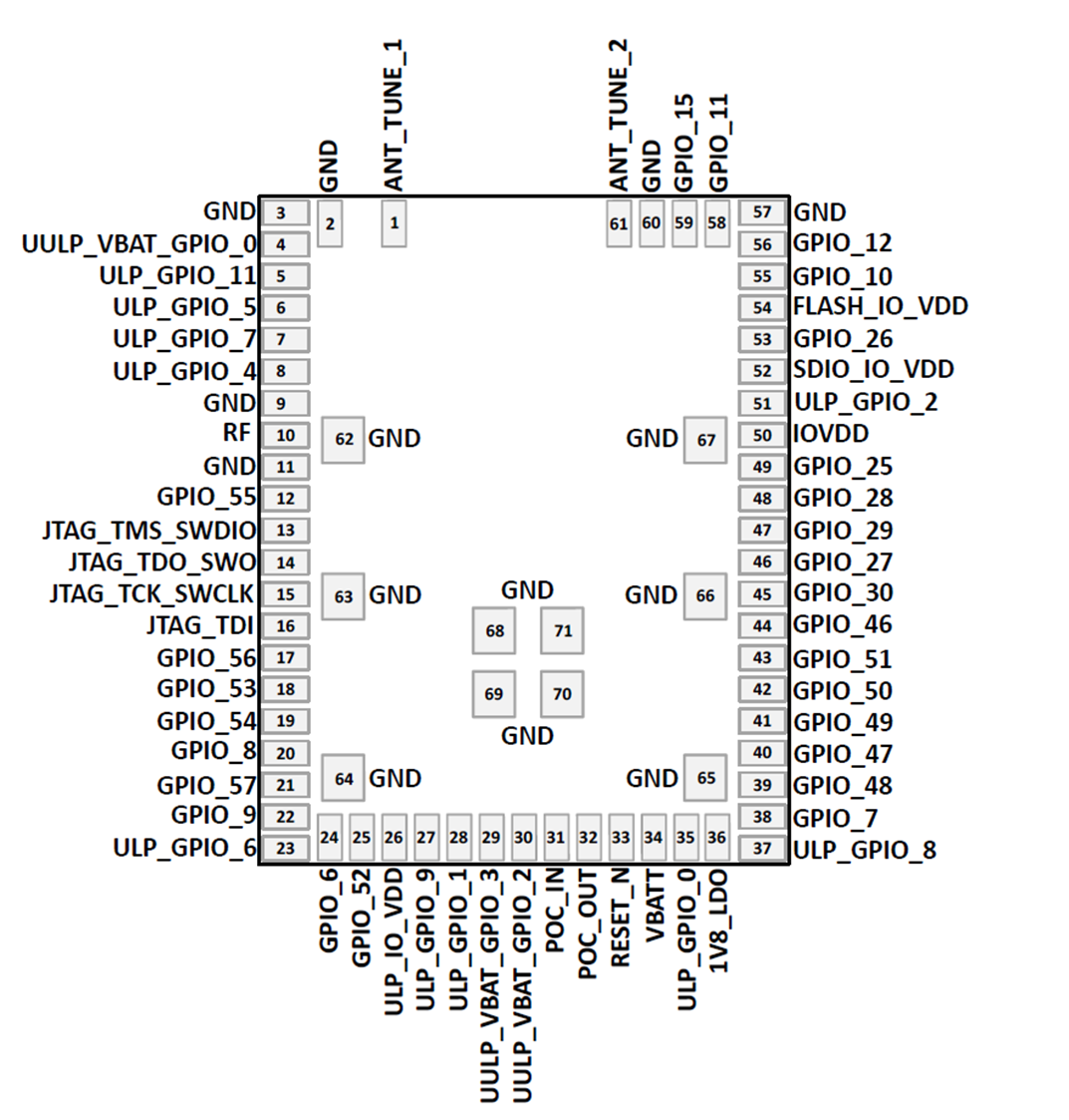
Package Outline
Module Dimensions
| Parameter | Value (LxWxH) | Units |
|---|---|---|
| Module Dimensions | 21.10 x 16 x 2.32 | mm |
| Tolerance | ±0.2 | mm |
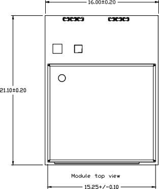


Pin Locations

Note: All coordinates below are in millimeters, and in TOP VIEW.
| Pad # | X | Y | Pad Size |
|---|---|---|---|
| 1 | -4 | 9.75 | (1.2 x 0.7) mm |
| 2 | -6 | 9.75 | |
| 3 | -7.2 | 10 | |
| 23 | -7.2 | -10 | |
| 24 | -6 | -9.75 | |
| 36 | 6 | -9.75 | |
| 37 | 7.2 | -10 | |
| 57 | 7.2 | -10 | |
| 58 | 6 | 9.75 | |
| 61 | 3 | 9.75 | |
| 62 | -5.5 | 3 | (1.2 x 1.2) mm |
| 63 | -5.5 | -2 | |
| 64 | -5.5 | -8 | |
| 65 | 5.5 | -8 | |
| 66 | 5.5 | -2 | |
| 67 | 5.5 | 3 | |
| 68 | -1 | -3 | |
| 69 | -1 | -5 | |
| 70 | 1 | -5 | |
| 71 | 1 | -3 |
PCB Landing Pattern

PCB Landing Pattern Pin Locations
| Pad # | X | Y | Pad Size |
|---|---|---|---|
| 1 | -4 | 10.05 | (1.8 x 0.7) mm |
| 2 | -6 | 10.05 | |
| 3 | -7.5 | 10 | |
| 23 | -7.5 | -10 | |
| 24 | -6 | -10.05 | |
| 36 | 6 | -10.05 | |
| 37 | 7.5 | -10 | |
| 57 | 7.5 | 10 | |
| 58 | 6 | 10.05 | |
| 61 | 3 | 10.05 | |
| 62 | -5.5 | 3 | (1.2 x 1.2) mm |
| 63 | -5.5 | -2 | |
| 64 | -5.5 | -8 | |
| 65 | 5.5 | -8 | |
| 66 | 5.5 | -2 | |
| 67 | 5.5 | 3 | |
| 68 | -1 | -3 | |
| 69 | -1 | -5 | |
| 70 | 1 | -5 | |
| 71 | 1 | -3 |
Mechanical Drawings
Heatsink (SOM Only?)
Schematics
Note:
Customers should include provision for programming or updating the firmware at manufacturing.
- If using UART, we recommend bringing out the SPI or SDIO lines to test points, so designers could use the faster interface for programming the firmware as needed.
- If using SPI or SDIO as host interface, then firmware programming or update can be done through the host MCU, or if design- er prefers to program standalone at manufacturing, then it is recommended to have test points on the SPI or SDIO signals.
- 3.3 V/1.8 V/VBATT must be supplied by external source.
- VBATT, SDIO_IO_VDD, IO_VDD, ULP_IO_VDD must be powered using External/On-board Power.
- FLASH_IO_VDD is powered by 1V8_LDO output.
- Place all the Caps closer to the corresponding Module pins.
453-00220 Schematics for Parts with RF Pin
System Supplies
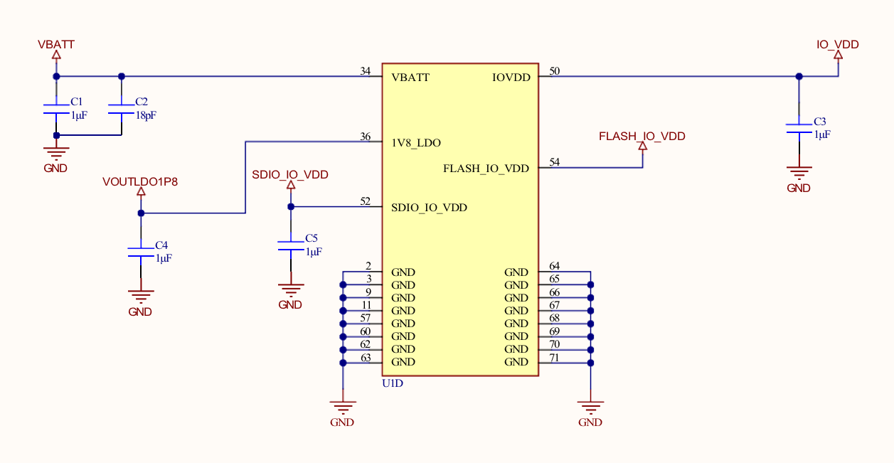
Note:
- Place all the decoupling capacitors close to the module pins.
- IO_VDD, SDIO_IO_VDD, ULP_IO_VDD can be powered independently by different voltage sources based on their corresponding signals voltage levels requirements. Voltages must be as per Recommended Operating Conditions.
- Even if GPIOs are not used, their respective IO domains must still be connected to the power supply.
RF, JTAG, and Reset Connection
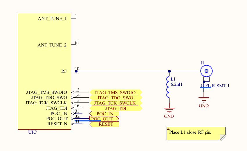
Note:
- Place L1 close to the RF pin.
- It is mandatory to follow the reference schematics for optimal RF performance.
- Maintain 50 ohm characteristic impedance for RF traces.
- J1: In-built antenna or an external antenna (with MHF4 connector) can be used.
- It is recommended to add microwave coaxial switch connector (Example : Murata's MM8430-2610RA1) or MHF4 connector for conducted measurements.
- Additional matching circuit to be provided near the antenna, based on antenna used and location on the board.
GPIO Connection
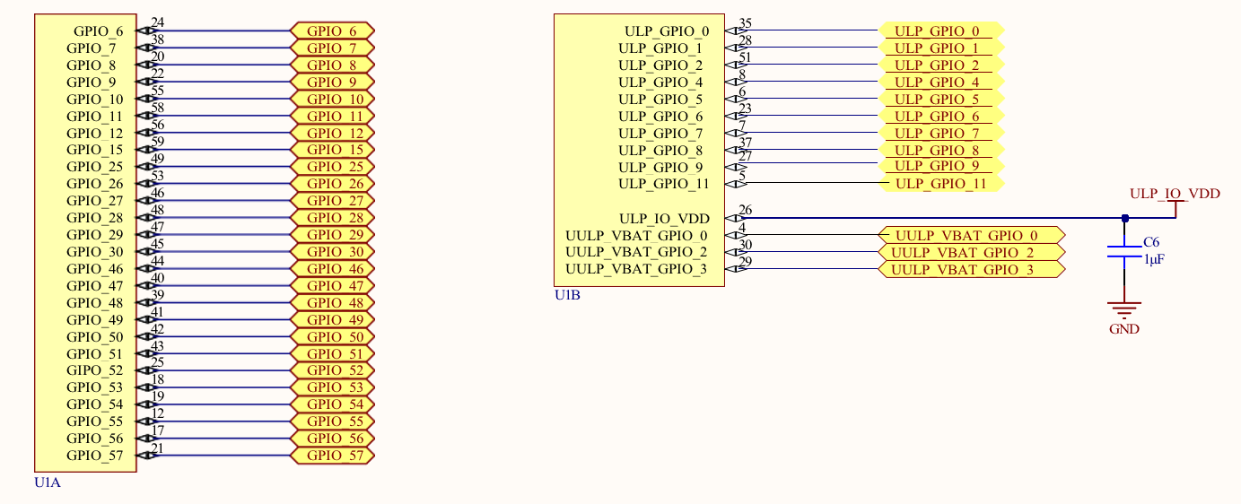
Note:
- Place all the decoupling capacitors close to the module pins.
- IO_VDD, SDIO_IO_VDD, ULP_IO_VDD can be powered independently by different voltage sources based on their corresponding signals voltage levels requirements. Voltages must be as per Recommended Operating Conditions.
- Even if GPIOs are not used, their respective IO domains must still be connected to the power supply.
- IO_VDD domain must be same as PSRAM supply in case of External PSRAM.
- Use recommended External PSRAM IC's as per the PSRAM section of the datasheet.
PSRAM and Flash configurations:
- If the module does not require external PSRAM and requires external Flash, then external flash can be connected to 46:51 or 52:57.
- If module requires external PSRAM and does not require external Flash, then external PSRAM can be connected to 46:51 or 52:57.
- If module requires both external flash and PSRAM, then external flash must be connected to 46:51, and external PSRAM must be connected to 52:57.
- The default pinset for external Flash is GPIO 46:51, while the default pinset for external PSRAM is GPIO 52:57.
- If either external Flash or external PSRAM is to be connected other than the default pinset, a change of MBR is required as described in UG574: SiWx917 SoC Manufacturing Utility User Guide, section 9.2.
- IO_VDD and its corresponding GPIOs in IO_VDD domain must be 1.8V when 1.8V external flash is used.
- IO_VDD and its corresponding GPIOs in IO_VDD domain must be 3.3V when 3.3V external flash is used.
- Use recommended External Flash ICs as per the Flash section of the datasheet.
- R5 through R10 are optional resistors for signal integrity.
- R5 33ohm on SDIO_CLK has to be near the source of the clock.
Reset
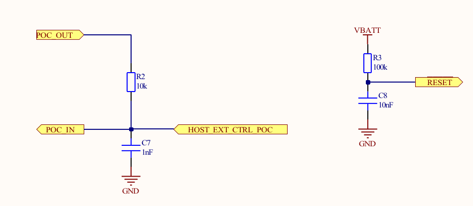
Note:
- The configuration shown allows for blackout monitor functionality along with external reset of the embedded SiWG917M IC.
- The POC_IN signal connects to the POC_IN pin on the SiWG917M. POC_IN resets all the internal blocks of the IC.
- The Si917_RESET signal connects to the RESET_N pin on the SiWG917M. It is recommended to use the RC filter as shown. RE- SET_N is an open-drain output pin that will be pulled low when POC_IN goes low.
- The POC_OUT signal connects to the POC_OUT pin on the SiWG917M. POC_OUT is an active-low, push-pull output from the internal blackout monitor. In this configuration, it is isolated from the external HOST_EXT_CTRL_POC signal with a series resistor. In applications without external host control (HOST_EXT_CTRL_POC), POC_OUT may be directly connected to POC_IN. Without external host control to the POC_IN pin, the IC cannot be reset multiple times after power-on.
- The HOST_EXT_CTRL_POC signal connects to a GPIO of an external host processor. In this configuration, HOST_EXT_CTRL_POC must be an open-drain output to allow POC_OUT to control POC_IN.
- HOST_EXT_CTRL_POC must be at the same voltage level as the VBATT supply pin.
LF Clock Option
Note: For WiFi, BLE, and Co-Ex power saving use cases & high accuracy MCU applications, Ezurio mandates an external clock to be used on UULP_VBAT_GPIO_3 pin for the low-frequency clock source to maintain timing accuracy requirements and optimize power consumption.
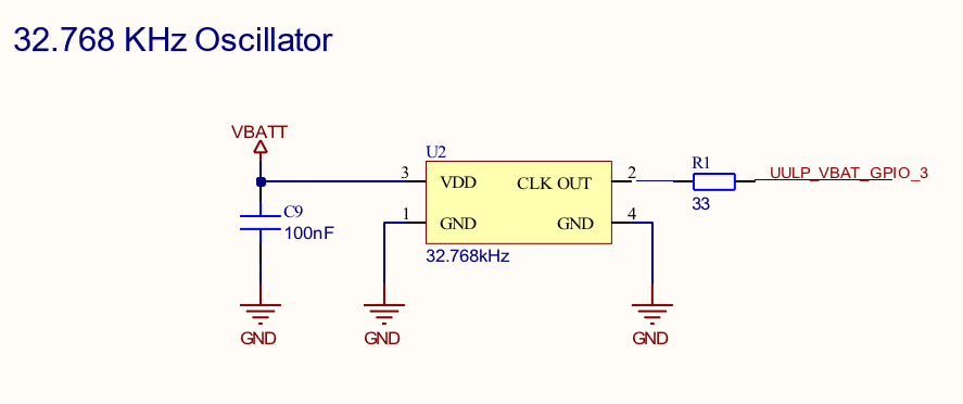
Flash Memory Configurations
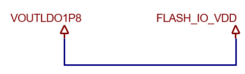
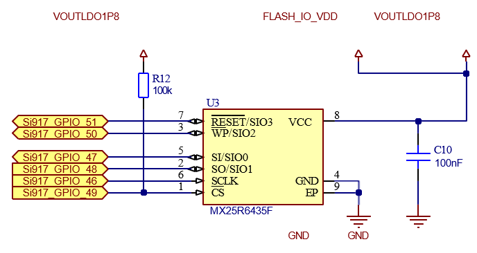
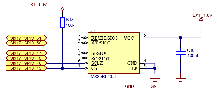
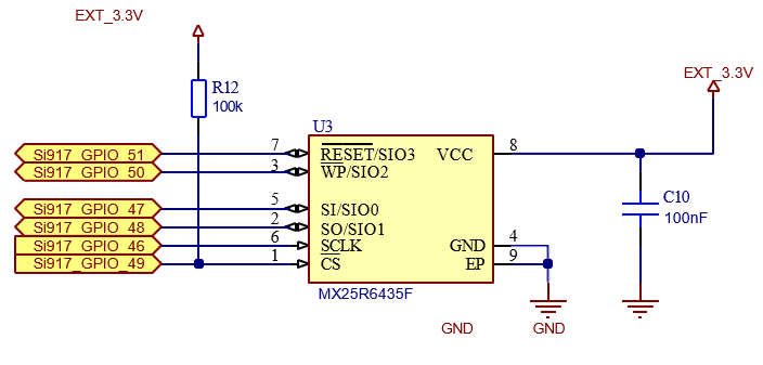
Note:
- Option 3 and Option 4 show single common flash to be used with both the NWP and MCU. A dual external flash configuration is also possible. The flash used for NWP must be connected to GPIO 46:51. A second external flash for MCU can be attached to GPIO 52:57.
- IO_VDD and its corresponding GPIOs in IO_VDD domain must be 1.8 V when 1.8 V external flash is used.
- IO_VDD and its corresponding GPIOs in IO_VDD domain must be 3.3 V when 3.3 V external flash is used.
- See SPI Flash Controllers for more information on external flash interface capabilities, and refer to AN1494: SiWx917 External Flash and PSRAM Application Note for recommended external flash ICs.
PSRAM Memory Configurations
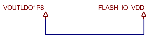
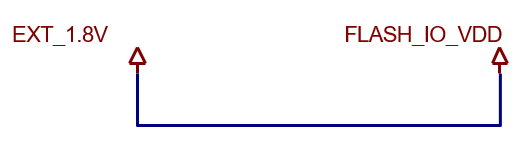
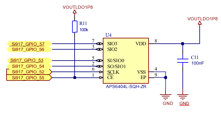
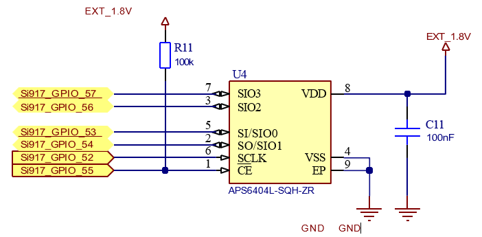
Note:
- IO_VDD and its corresponding GPIOs in the IO_VDD domain must be same as PSRAM supply in case of external PSRAM.
- Either GPIO 46:51 or GPIO 52:57 can be used as the external PSRAM interface. For external common flash mode, the flash de- vice must be connected to GPIO 46:51, and PSRAM must be connected to GPIO 52:57.
- Standby associated current numbers vary based on the above option used.
- The reference schematics represent a sample of configurations. See Flash and PSRAM Supply Connections for more details on possible configurations.
- Refer to AN1494: SiWx917 External Flash and PSRAM Application Note for recommended external PSRAM ICs.
Debug and In-System Programming
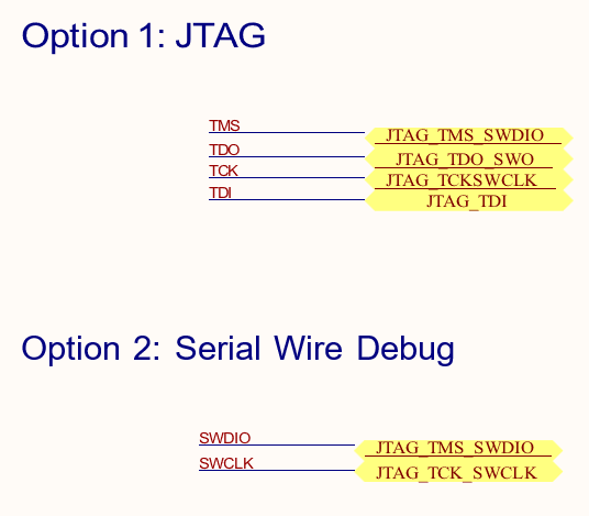
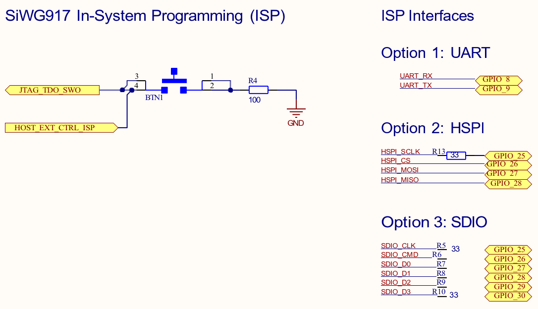
Note:
- In UART mode, ensure that the input signal, UART_RX is not floating when the device is powered up and reset is deasserted. This can be done by ensuring that the host processor configures its signals (outputs) before deasserting the reset.
In HSPI mode, ensure that the input signals, HSPI_CS and HSPI_CLK are not floating when the device is powered up and reset is deasserted. This can be done by ensuring that the external Host processor configures its signals (outputs) before deasserting the reset. HSPI_INTR is the interrupt signal driven by the secondary device. This signal may be configured as Active-high or Active- low. If it is active-high, an external pull-down resistor is required. If it is active-low, an external pull-up resistor is required.
The following actions can be carried out by the host processor during power-up of the device, and before/after ULP Sleep mode.- To use the signal in the Active-high or Active-low mode, ensure that during the power up of the device, the Interrupt is disabled in the Host processor before deasserting the reset. After deasserting the reset, the Interrupt needs to be enabled only after the HSPI initialization is done and the Interrupt mode is programmed to either Active-high or Active-low mode as required.
- The Host processor needs to disable the interrupt before the ULP Sleep mode is entered and enable it after SPI interface is reinitialized upon wakeup from ULP Sleep.
- In SDIO mode, pull-up resistors should be present on SDIO_CMD & SDIO Data lines as per the SDIO physical layer specification version 2.0.
- R5 to R10 and R13 are optional resistors for signal integrity.
- 33ohm on SDIO_CLK/HSPI_CLK has to be near the source of the clock, and not near the module.
Bill of Materials
Bill of Materials
| Line No | Quantity | Designator | Value | Description | Manufacturer | Manufacturer PN | Tolerance | Rating |
|---|---|---|---|---|---|---|---|---|
| 1 | 5 | C1, C3, C4, C5, C6 | 1uF | CAP CER 0402 X5R 1uF 10V 10% | - | - | 10% | 10 V |
| 2 | 1 | C2 | 18pF | CAP CER 0201 C0G 18pF 25V 2% | - | - | 2% | 25V |
| 3 | 1 | C7 | 1nF | CAP CER 0402 X7R 1nF 16V 10% | - | - | 10% | 16V |
| 4 | 1 | C8 | 10nF | CAP CER 0402 X7R 10nF 16V 10% | - | - | 10% | 16V |
| 5 | 1 | C9 | 100nF | CAP CER 0402 X7R 100nF 50V 10% | - | - | 10% | 50V |
| 6 | 1 | J1 | U.FL-R- SMT-1 | CONN RF 500HM UFL_2.6x2.6 SMD | - | - | ||
| 7 | 1 | L1 | 6.2 nH | IND Fixed 0201 6.2nH 300mA 600mOhm 3% | - | - | 3% | 300mA |
| 8 | 8 | R1, R5, R6, R7, R8, R9, R10, R13 | 33 | RES 0402 33R 1/16W 1% 100ppm | - | - | 1% | 62.5 mW |
| 9 | 1 | R2 | 10k | RES 0402 10K 1/16W 5% 200ppm | - | - | 5% | 63mW |
| 10 | 2 | R3, R12 | 100k | RES 0402 100K 1/16W 1% 100ppm | - | - | 1% | 63mW |
| 11 | 1 | R4 | 100 | RES 0402 100R 1/16W 1% 100ppm | - | - | 1% | 63mW |
| 12 | 1 | BTN1 | PTS810 SJM 250 SMTR LFS | C&K Tactile Switch SPST-NO 0.05A 16V | C&K | PTS810 SJM 250 SMTR LFS | ||
| 13 | 1 | U2 | 32.768 kHz | SiTIME CRYSTAL CSPBGA 32.768kHz 10pF 100ppm | SiTIME | SiT1532A I-J4- DCC-32.7 68 | ||
| 14 | 1 | U1 | 453-00220 | SL917 Module 453-00220 | Ezurio |
SL917: External Flash & PSRAM BOM Options (these are optional and need not be used for every use-case)
| Designator | Value | Manufacturer | Manufacturer PN | Description |
|---|---|---|---|---|
| U3 | MX25R6435F | Macronix | MX25R6435FM2IL0 | IC FLASH 64MBIT SPI/ QUAD 8SOP |
| U4 | APS6404L-SQH-ZR | AP Memory | APS6404L-SQH-ZR | IC PSRAM 64Mbit QSPI USON |
| R11, R12 | 100k | - | - | RES 0402 100K 1/16W 1% 100ppm |
| C10, C11 | 100nF | - | - | CAP CER 0402 X7R 100nF 50V 10% |
453-00222 Schematics for parts with Integral Antenna
System Supplies
Note:
- Place all the decoupling capacitors close to the module pins.
- IO_VDD, SDIO_IO_VDD, ULP_IO_VDD can be powered independently by different voltage sources based on their corresponding signals voltage levels requirements. Voltages must be as per Recommended Operating Conditions.
- Even if GPIOs are not used, their respective IO domains must still be connected to the power supply.
RF, JTAG, and Reset Connection

Note:
- It is mandatory to follow the reference schematics for optimal RF performance.
GPIO Connection
Note:
- Place all the decoupling capacitors close to the module pins.
- IO_VDD, SDIO_IO_VDD, ULP_IO_VDD can be powered independently by different voltage sources based on their corresponding signals voltage levels requirements. Voltages must be as per Recommended Operating Conditions.
- Even if GPIOs are not used, their respective IO domains must still be connected to the power supply.
- IO_VDD domain must be same as PSRAM supply in case of External PSRAM.
- Use recommended External PSRAM IC's as per the PSRAM section of the datasheet.
PSRAM and Flash configurations:
- If the module does not require external PSRAM and requires external Flash, then external flash can be connected to 46:51 or 52:57.
- If module requires external PSRAM and does not require external Flash, then external PSRAM can be connected to 46:51 or 52:57.
- If module requires both external flash and PSRAM, then external flash must be connected to 46:51, and external PSRAM must be connected to 52:57.
- The default pinset for external Flash is GPIO 46:51, while the default pinset for external PSRAM is GPIO 52:57.
- If either external Flash or external PSRAM is to be connected other than the default pinset, a change of MBR is required as described in UG574: SiWx917 SoC Manufacturing Utility User Guide, section 9.2.
- IO_VDD and its corresponding GPIOs in IO_VDD domain must be 1.8V when 1.8V external flash is used.
- IO_VDD and its corresponding GPIOs in IO_VDD domain must be 3.3V when 3.3V external flash is used.
- Use recommended External Flash IC's as per the Flash section of the datasheet.
Reset
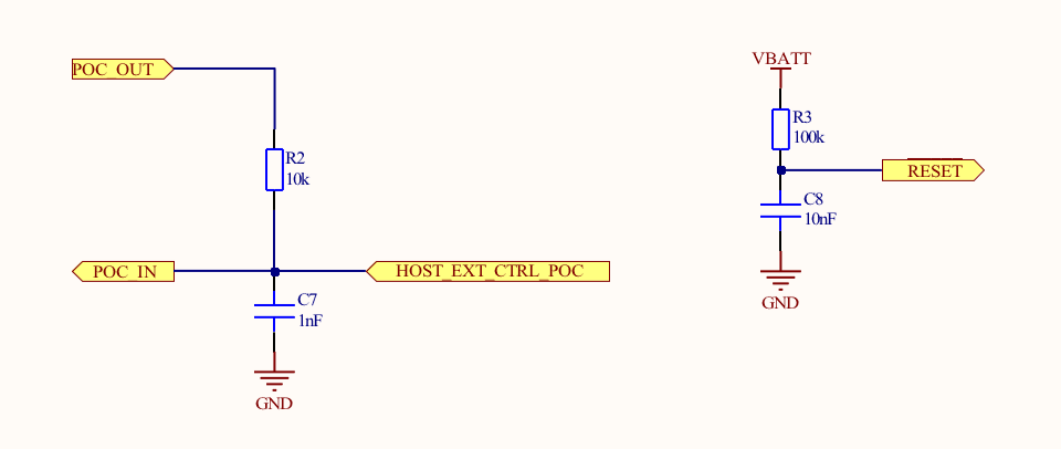
Note:
- The configuration shown allows for blackout monitor functionality along with external reset of the embedded SiWG917M IC.
- The POC_IN signal connects to the POC_IN pin on the SiWG917M. POC_IN resets all the internal blocks of the IC.
- The Si917_RESET signal connects to the RESET_N pin on the SiWG917M. It is recommended to use the RC filter as shown. RESET_N is an open-drain output pin that will be pulled low when POC_IN goes low.
- The POC_OUT signal connects to the POC_OUT pin on the SiWG917M. POC_OUT is an active-low, push-pull output from the internal blackout monitor. In this configuration, it is isolated from the external HOST_EXT_CTRL_POC signal with a series resistor. In applications without external host control (HOST_EXT_CTRL_POC), POC_OUT may be directly connected to POC_IN. Without external host control to the POC_IN pin, the IC cannot be reset multiple times after power-on.
- The HOST_EXT_CTRL_POC signal connects to a GPIO of an external host processor. In this configuration, HOST_EXT_CTRL_POC must be an open-drain output to allow POC_OUT to control POC_IN.
- HOST_EXT_CTRL_POC must be at the same voltage level as the VBATT supply pin.
LF Clock Option
Note: For WiFi, BLE, and Co-Ex power saving use cases & high accuracy MCU applications, Ezurio mandates an external clock to be used on UULP_VBAT_GPIO_3 pin for the low-frequency clock source to maintain timing accuracy requirements and optimize power consumption.
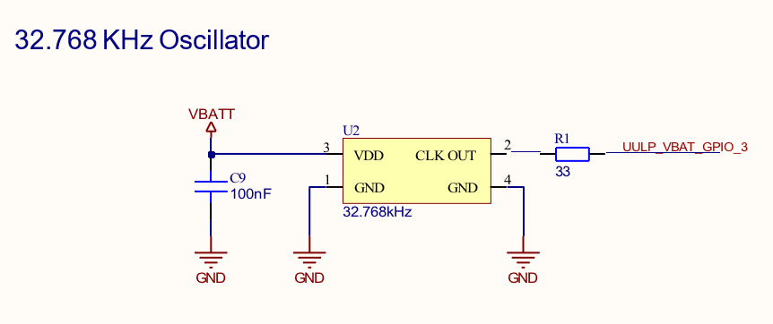
Flash Memory Configurations


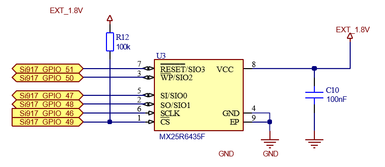
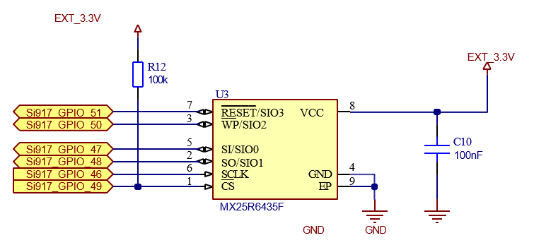
Note:
- Option 3 and Option 4 show single common flash to be used with both the NWP and MCU. A dual external flash configuration is also possible. The flash used for NWP must be connected to GPIO 46:51. A second external flash for MCU can be attached to GPIO 52:57.
- IO_VDD and its corresponding GPIOs in IO_VDD domain must be 1.8 V when 1.8 V external flash is used.
- IO_VDD and its corresponding GPIOs in IO_VDD domain must be 3.3 V when 3.3 V external flash is used.
- See SPI Flash Controllers for more information on external flash interface capabilities, and refer to AN1494: SiWx917 External Flash and PSRAM Application Note for recommended external flash ICs.
PSRAM Memory Configurations

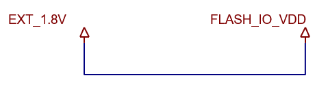
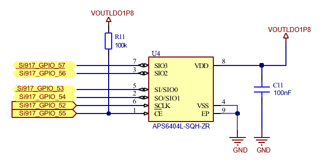
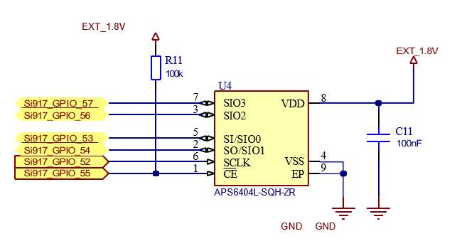
Note:
- IO_VDD and its corresponding GPIOs in the IO_VDD domain must be same as PSRAM supply in case of external PSRAM.
- Either GPIO 46:51 or GPIO 52:57 can be used as the external PSRAM interface. For external common flash mode, the flash de- vice must be connected to GPIO 46:51, and PSRAM must be connected to GPIO 52:57.
- Standby associated current numbers vary based on the above option used.
- The reference schematics represent a sample of configurations. See Flash and PSRAM Supply Connections for more details on possible configurations.
- Refer to AN1494: SiWx917 External Flash and PSRAM Application Note for recommended external PSRAM ICs.
Debug and In-System Programming
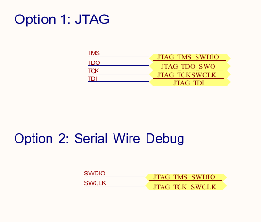
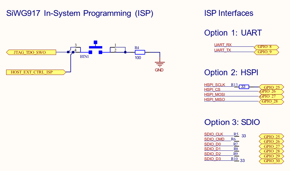
Note:
- In UART mode, ensure that the input signal, UART_RX is not floating when the device is powered up and reset is deasserted. This can be done by ensuring that the host processor configures its signals (outputs) before deasserting the reset.
In HSPI mode, ensure that the input signals, HSPI_CS and HSPI_CLK are not floating when the device is powered up and reset is deasserted. This can be done by ensuring that the external Host processor configures its signals (outputs) before deasserting the reset. HSPI_INTR is the interrupt signal driven by the secondary device. This signal may be configured as Active-high or Active- low. If it is active-high, an external pull-down resistor is required. If it is active-low, an external pull-up resistor is required.
The following actions can be carried out by the host processor during power-up of the device, and before/after ULP Sleep mode.- To use the signal in the Active-high or Active-low mode, ensure that during the power up of the device, the Interrupt is disabled in the Host processor before deasserting the reset. After deasserting the reset, the Interrupt needs to be enabled only after the HSPI initialization is done and the Interrupt mode is programmed to either Active-high or Active-low mode as required.
- The Host processor needs to disable the interrupt before the ULP Sleep mode is entered and enable it after SPI interface is reinitialized upon wakeup from ULP Sleep.
- In SDIO mode, pull-up resistors should be present on SDIO_CMD & SDIO Data lines as per the SDIO physical layer specification version 2.0.
- R5 to R10 and R13 are optional resistors for signal integrity.
- 33ohm on SDIO_CLK/HSPI_CLK has to be near the source of the clock, and not near the module.
Bill of Materials
Bill of Materials
| Line No | Quantity | Designator | Value | Description | Manufacturer | Manufacturer PN | Tolerance | Rating |
|---|---|---|---|---|---|---|---|---|
| 1 | 5 | C1, C3, C4, C5, C6 | 1uF | CAP CER 0402 X5R 1uF 10V 10% | - | - | 10% | 10 V |
| 2 | 1 | C2 | 18pF | CAP CER 0201 C0G 18pF 25V 2% | - | - | 2% | 25V |
| 3 | 1 | C7 | 1nF | CAP CER 0402 X7R 1nF 16V 10% | - | - | 10% | 16V |
| 4 | 1 | C8 | 10nF | CAP CER 0402 X7R 10nF 16V 10% | - | - | 10% | 16V |
| 5 | 1 | C9 | 100nF | CAP CER 0402 X7R 100nF 50V 10% | - | - | 10% | 50V |
| 6 | 1 | J1 | U.FL-R- SMT-1 | CONN RF 500HM UFL_2.6x2.6 SMD | - | - | ||
| 7 | 1 | L1 | 6.2 nH | IND Fixed 0201 6.2nH 300mA 600mOhm 3% | - | - | 3% | 300mA |
| 8 | 8 | R1, R5, R6, R7, R8, R9, R10, R13 | 33 | RES 0402 33R 1/16W 1% 100ppm | - | - | 1% | 62.5 mW |
| 9 | 1 | R2 | 10k | RES 0402 10K 1/16W 5% 200ppm | - | - | 5% | 63mW |
| 10 | 2 | R3, R12 | 100k | RES 0402 100K 1/16W 1% 100ppm | - | - | 1% | 63mW |
| 11 | 1 | R4 | 100 | RES 0402 100R 1/16W 1% 100ppm | - | - | 1% | 63mW |
| 12 | 1 | BTN1 | PTS810 SJM 250 SMTR LFS | C&K Tactile Switch SPST-NO 0.05A 16V | C&K | PTS810 SJM 250 SMTR LFS | ||
| 13 | 1 | U2 | 32.768 kHz | SiTIME CRYSTAL CSPBGA 32.768kHz 10pF 100ppm | SiTIME | SiT1532A I-J4- DCC-32.7 68 | ||
| 14 | 1 | U1 | 453-00222 | SL917 Module 453-00222 | Ezurio |
External Flash & PSRAM BOM Options (these are optional and need not be used for every use-case)
| Designator | Value | Manufacturer | Manufacturer PN | Description |
|---|---|---|---|---|
| U3 | MX25R6435F | Macronix | MX25R6435FM2IL0 | IC FLASH 64MBIT SPI/ QUAD 8SOP |
| U4 | APS6404L-SQH-ZR | AP Memory | APS6404L-SQH-ZR | IC PSRAM 64Mbit QSPI USON |
| R11, R12 | 100k | - | - | RES 0402 100K 1/16W 1% 100ppm |
| C10, C11 | 100nF | - | - | CAP CER 0402 X7R 100nF 50V 10% |
Layout Guidelines
- The RF (Module Pin No. 10) signal may be directly connected to an on-board chip antenna or terminated in an RF pin connector of any form factor for enabling the use of external antennas. RF pin can be left floating if not used.
- Antenna clearance area is not necessary if you are using an external antenna attached to the RF pin.
- The RF pin trace on RF pin should have a characteristic impedance of 50 Ohms. Any standard 50 Ohms RF pin trace (Microstrip or Coplanar wave guide) may be used. The width of the 50 Ohms line depends on the PCB stack, e.g., the dielectric of the PCB, thickness of the copper, thickness of the dielectric and other factors. Consult the PCB fabrication unit to get these factors right.
- To evaluate transmit and receive performance like Tx Power, and EVM and Rx sensitivity, an RF pin connector would be required. A suggestion is to place a ‘microwave coaxial connector with switch’ between RF pin and the antenna.
- Each GND pin must have a separate GND via. Place the ground vias as close to the ground pads as possible.
- All decoupling capacitors placement must be as much close as possible to the corresponding power pins, and the trace lengths as short as possible.
- Ensure all power supply traces widths are sufficient enough to carry corresponding currents.
- Add GND copper pour underneath IC/Module in all layers, for better thermal dissipation.
- Add solid GND copper pour underneath Module for better emission performance.
Electrical Characteristics
Absolute Maximum Ratings
Stresses beyond those listed below may cause permanent damage to the device. This is a stress rating only and functional operation of the devices at those or any other conditions beyond those indicated in the operation listings of this specification is not implied. Exposure to maximum rating conditions for extended periods may affect device reliability. For more information on the available quality and reliability data, see the Quality and Reliability Monitor Report at https://www.silabs.com/about-us/quality .
Note: All the specifications are preliminary and subject to change.
| Parameter | Symbol | Test Conditon | Min | Typ | Max | Unit |
|---|---|---|---|---|---|---|
| Storage temperature | Tstore | -40 | — | 125 | oC | |
| Maximum junction temperature | Tj(max) | — | 125 | oC | ||
| 3.3V power supply for the on-chip Buck, RF circuit, and UULP IOs | VBATT | -0.5 | — | 3.63 | V | |
| I/O supply for GPIOs | IO_VDD | -0.5 | — | 3.63 | V | |
| I/O supply for SDIO I/Os | SDIO_IO_VDD | -0.5 | — | 3.63 | V | |
| I/O supply for QSPI flash signals | FLASH_IO_VDD | -0.5 | — | 3.63 | V | |
| I/O supply for ULP I/Os | ULP_IO_VDD | -0.5 | — | 3.63 | V | |
| DC voltage on any I/O pin 1 | VIO_PIN | -0.5 | — | VDD + 0.5 | V | |
| Total average max current into chip | Ipmax | — | — | 500 | mA | |
| Current per I/O pin | IIOMAX | Sink | — | — | 100 | mA |
| Source | — | — | 100 | mA |
Note:
- VDD = I/O supply domain pin. Refer to pin description tables for supply domain associated with each I/O.
Recommended Operating Conditions
Note: The device may operate continuously at the maximum allowable ambient Tambient rating as long as the maximum junction Tjunction(max) is not exceeded. For an application with significant power dissipation, the allowable Tambient may be lower than the maximum Tambient rating. Tambient = Tjunction(max) - (ΘJA x Power Dissipation). Refer to the Thermal Characteristics table for ΘJA.
| Parameter | Symbol | Test Condition | Min. | Typ. | Max. | Units |
|---|---|---|---|---|---|---|
| Ambient temperature | Tambient | -40 | 25 | 85 | oC | |
| Junction temperature | Tjunction | 105 | oC | |||
| 3.3V power supply for the on- chip Buck, RF Power Amplifier, UULP I/Os | VBATT | 3.0 | 3.3 | 3.63 | V | |
| I/O supply for Flash | FLASH_IO_VD D | 1.71 | 1.8 | 1.98 | V | |
| I/O supply for GPIOs | IO_VDD1 | 1.8 V nominal operation | 1.71 | 1.8 | 1.98 |
V |
| 3.3 V nominal operation | 2.97 | 3.3 | 3.63 | |||
I/O supply for SDIO I/Os |
SDIO_IO_VDD1 | 1.8 V nominal operation | 1.71 | 1.8 | 1.98 |
V |
| 3.3 V nominal operation | 2.97 | 3.3 | 3.63 | |||
| I/O supply for ULP I/Os | ULP_IO_VDD1 | 1.8 V nominal operation | 1.71 | 1.8 | 1.98 |
V |
| 3.3 V nominal operation | 2.97 | 3.3 | 3.63 |
Note:
- Supplies can operate at a nominal 3.3 V or 1.8 V level independent of the other supplies in the system.
DC Electrical Characteristics
RESET_N Pin
| Parameter | Symbol | Test Condition | Min | Typ | Max | Unit |
|---|---|---|---|---|---|---|
| High level input voltage | VIH | RESET_N pin, VBATT = 3.3 V | 0.8 * VBATT | — | — | V |
| Low level input voltage | VIL | RESET_N pin, VBATT = 3.3 V | — | — | 0.3 * VBATT | V |
Power On Control (POC) and Reset
There are three signals involved in power-on control and reset of the device:
- POC_IN: When pulled low, POC_IN will reset all of the internal blocks in the device. The POC_IN signal can be controlled either by external circuitry, by POC_OUT, or both.
- RESET_N: RESET_N is an open-drain signal which will be pulled low during a chip reset. It is released after POC_IN is high. RE- SET_N should be connected to an RC circuit to fulfill the timing requirements shown below.
- POC_OUT: The POC_OUT signal is the output of the internal blackout supply monitor. POC_OUT is distributed to all I/O cells to prevent the I/O cells from powering up in an undesired configuration and is also used inside the IC to place the IC in a safe state until a valid supply is available for proper operation. During power up, POC_OUT stays low until the VBATT reaches 1.6 V. After the VBATT supply exceeds 1.6 V, POC_OUT becomes high and normal operation begins. If VBATT becomes lower than the blackout threshold voltage, POC_OUT will return low. POC_OUT can be used to provide chip reset by connecting to POC_IN in a loopback configuration.
The recommended schematic for the reset signals is shown in Figure 8.4 Reset Configuration on page 142.
Below shows the signal timing when POC_OUT, POC_IN, and RESET_N are connected per the recommended schematic. The POC_IN-to-RESET_N delay will occur when POC_IN transitions low to high.
In this configuration the system only has to control the supply (VBATT) during power-up and power down and need not control POC_IN externally. On power-up the chip will be reset internally. The power-down sequence will follow VBATT and external control of POC_IN is not required.
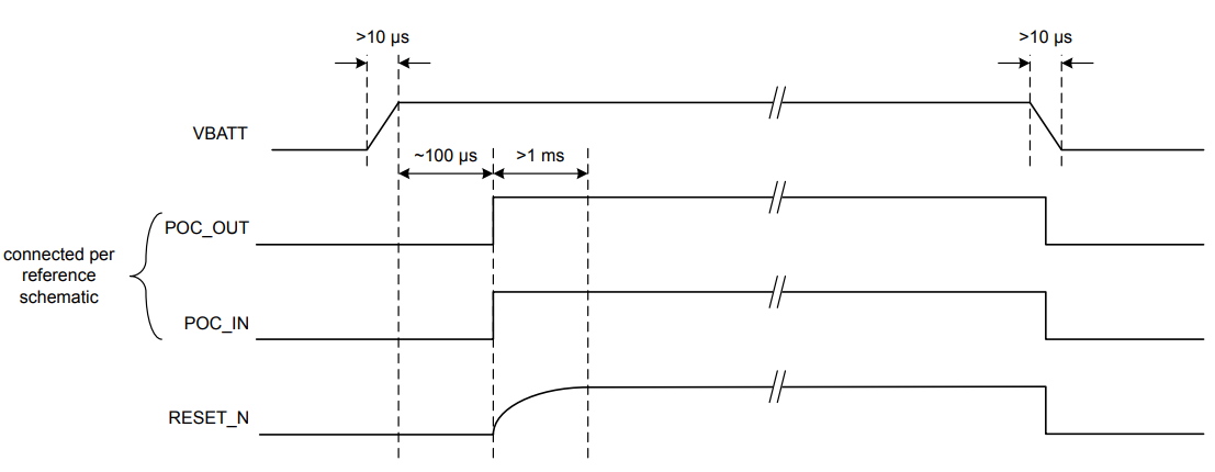
If the chip is to be reset from an external host device while powered up, the POC_IN signal should be pulled low for at least 10 ms as shown below. Upon release of POC_IN, the POC_IN-to-RESET_N delay will occur.
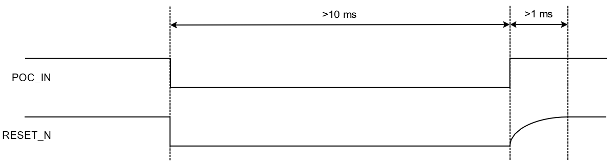
In the above timing diagrams, it is assumed that all supplies including VBATT are connected together. If they are not connected together and independently controlled, then the guidance below must be followed.
Case1: POC is looped back and there is no external control for POC_IN
- All supplies can be enabled at the same time, if possible
- If supplies cannot be enabled at the same time, the VBATT supplies should be powered up first and all other supplies should be powered on at least 1 ms before RESET_N is high. The RC circuit controlling RESET_N must be adjusted to provide the appropriate delay.
- While powering down, supplies can be powered off simultaneously, or with VBATT the last to be disabled.
Case2: POC is looped back and there is external control for POC_IN during power-up / power-down.
- All supplies can be enabled at the same time, or VBATT may be enabled before other supplies.
- POC_IN should be kept low for at least 600 us after all the supplies have settled.
- On power-down, POC_IN can be driven low before disabling the supplies. Supplies can be powered off simultaneously, or with VBATT the last to be disabled.
Blackout Monitor
The blackout comparator is enabled by default upon power up. Blackout is typically asserted when the UULP_VBATT_1 or UULP_VBATT2 (VBATT) supply goes lower than 1.6 V (see Table 7.4 Blackout Monitor Electrical Specifications on page 95), and it is de-asserted when VBATT supply goes higher than 1.625 V. The blackout monitor circuit will reset the device when POC_OUT is connected to POC_IN as recommended.
The blackout monitor will be disabled after power up. The functionality should be enabled by the SoC firmware if required in the system. The blackout monitor block should be enabled to monitor the VBATT voltage only in high power modes. In low power modes battery level detection can be implemented using the Nano-Power Brownout detection comparator.
When the system is in low power mode, the blackout comparator is automatically enabled upon a brownout event.
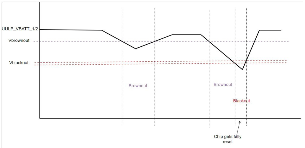
Blackout Monitor Electrical Specifications
| Parameter | Symbol | Test Condition | Min | Typ | Max | Unit |
|---|---|---|---|---|---|---|
| VBATT voltage at which the Blackout monitor resets the IC | VTLblackout | — | 1.56 | 1.65 | V | |
| VBATT voltage at which the Blackout monitor releases the IC from reset | VTHblackout | — | 1.59 | 1.675 | V |
Nano Power Comparator and Brown Out Detection (BOD)
The Nano Power comparator subsystem consists of a sampled comparator, reference buffer and resistor bank.
Features
- Battery voltage measurement
- Brownout detection
- Three button wakeup is supported using single VOLT_SENSE signal
Nano Power BOD Electrical Specifications
| Parameter | Symbol | Test Condition | Min | Typ | Max | Unit |
|---|---|---|---|---|---|---|
| Battery status accuracy | Vbatt_status | — | +/-100 | — | mV | |
| Brownout detection accuracy | VBOD | — | +/-100 | — | mV |
Digital I/O Signals
| Parameter | Symbol | Test Condition | Min | Typ | Max | Unit |
|---|---|---|---|---|---|---|
| High level input voltage | VIH | IO_VDDx = 3.3 V | 2 | — | — | V |
| IO_VDDx = 1.8 V | 1.17 | — | — | V | ||
| Low level input voltage | VIL | IO_VDDx = 3.3 V | — | — | 0.8 | V |
| IO_VDDx = 1.8 V | — | — | 0.63 | V | ||
| Low level output voltage | VOL | — | — | 0.4 | V | |
| High level output voltage | VOH | IO_VDDx - 0.4 | — | — | V | |
| Low level output current (programmable) | IOL | GPIO_* and ULP_GPIO_* pins | 2 | 4 | 12 | mA |
| UULP_GPIO_* pins | 1 | — | 2 | mA | ||
| High level output current (programmable) | IOH | GPIO_* and ULP_GPIO_* pins | 2 | 4 | 12 | mA |
| UULP_GPIO_* pins | 1 | — | 2 | mA | ||
| Pull-up resistance | RPU | GPIO_* and ULP_GPIO_* pins | — | 53 | — | kΩ |
| Pull-down resistance | RPD | GPIO_* and ULP_GPIO_* pins | — | 63 | — | kΩ |
Open-Drain I2C Pins
| Parameter | Symbol | Test Condition | Min | Typ | Max | Unit |
|---|---|---|---|---|---|---|
| High level input voltage | VIH | 0.7 * IO_VDDx | — | — | V | |
| Low level input voltage | VIL | — | — | 0.3 * IO_VDDx | V |
Flash LDO Electrical Specifications - Regulation Mode
| Parameter | Symbol | Test Condition | Min | Typ | Max | Unit |
| Input Supply Voltage (VBATT) | Vin | Flash LDO in Regulation Mode | 2.97 | 3.3 | 3.63 | V |
| Output Voltage Range (VBATT) | Vout | — | 1.8 | — | V | |
| Load current | Iload | — | — | 48 | mA | |
| Line Regulation | REGline | Vin Changed from 2.97 V to 3.63 V | — | — | 0.6 | % |
| Load Regulation | REGload | Iload changed from 0 mA to 48 mA | — | — | 1.4 | % |
AC Characteristics
Clock Specifications
The SL917 SoC modules require two primary clocks:
Low frequency 32 kHz clock for sleep manager and RTC
- Internal 32 kHz RC clock may be used for applications with low timing accuracy requirements
- 32.768 kHz LVCMOS rail-to-rail external oscillator input pin UULP_VBAT_GPIO_3 for external oscillator or host clock
High frequency 40 MHz clock for NWP, Cortex-M4, baseband subsystem and the radio
- 40 MHz clock is integrated inside the module, and no external clock needs to be provided
The chipsets have integrated internal oscillators including crystal oscillators to generate the required clocks. Integrated crystal oscillators enable the use of low-cost passive crystal components. Additionally, in a system where an external clock source is already present, the clock can be reused. The following are the recommended options for the clocks for different functionalities:
32 kHz External Sources:
Note:
- For WiFi, BLE, and Co-Ex power saving use cases & high accuracy MCU applications, Ezurio mandates an external clock to be used on UULP_VBAT_GPIO_3 pin for the low-frequency clock source to maintain timing accuracy requirements and optimize power consumption.
- Option 1: From Host MCU/MPU LVCMOS rail to rail clock input on UULP_VBAT_GPIO_3
- Option 2: External clock oscillator providing LVCMOS rail to rail clock input on UULP_VBAT_GPIO_3 (Nano-drive clock should not be supplied)."
Low Frequency Clock
Low-frequency clock selection can be done through software. The RC oscillator clock is not suited for high timing accuracy applications and may increase overall system current consumption in duty-cycled power modes.
32kHZ Internal RC Oscillator
| Parameter | Symbol | Test Condition | Min | Typ | Max | Unit |
|---|---|---|---|---|---|---|
| Oscillator Frequency | Fosc | 32.0 | kHz | |||
| Frequency Variation with Temp and Voltage | Fosc_Acc | 1.2 | % |
32.768 kHz External Oscillator
An external 32.768 kHz low-frequency clock can be fed through UULP_VBAT_GPIO_3.
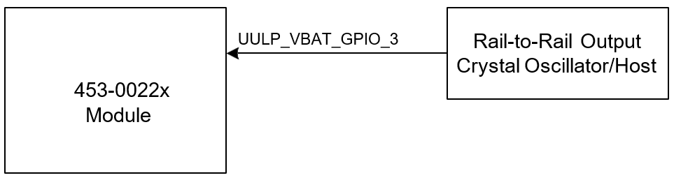
Oscillator Specifications
| Parameter | Symbol | Test Condition | Min | Typ | Max | Unit |
|---|---|---|---|---|---|---|
| Oscillator Frequency | fosc | — | 32.768 | — | kHz | |
| Frequency Variation with Temp and Voltage | fosc_Acc | -100 | — | 100 | ppm | |
| Input duty cycle | DCin | 30 | 50 | 70 | % | |
| Input AC peak-peak voltage swing at input pin. | VAC | -0.3 | — | VBATT +/- 10% | Vpp |
SDIO 2.0 Secondary
Full Speed Mode
SDIO 2.0 Secondary Full Speed Mode
| Parameter | Symbol | Test Condition | Min | Typ | Max | Unit |
|---|---|---|---|---|---|---|
| SDIO_CLK | fsdio_clk | — | — | 25 | MHz | |
| SDIO_DATA, SDIO_CMD input setup time | ts | 4 | — | — | ns | |
| SDIO_DATA, SDIO_CMD input hold time | th | 1.2 | — | — | ns | |
| SDIO_DATA, clock to output delay | tod | — | — | 13 | ns | |
| Output Load | CL | 5 | — | 10 | pF |
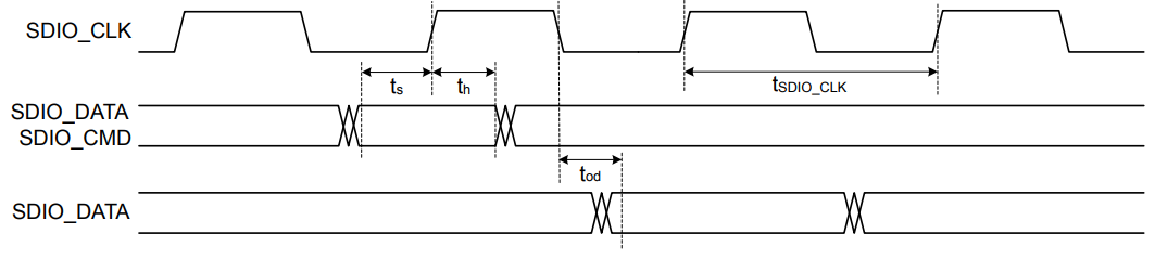
High Speed Mode
SDIO 2.0 Secondary High Speed Mode
| Parameter | Symbol | Test Condition | Min | Typ | Max | Unit |
|---|---|---|---|---|---|---|
| SDIO_CLK | fsdio_clk | 25 | — | 50 | MHz | |
| SDIO_DATA, input setup time | ts | 4 | — | — | ns | |
| SDIO_DATA, input hold time | th | 1.2 | — | — | ns | |
| SDIO_DATA, clock to output delay | tod | 2.5 | — | 13 | ns | |
| Output Load | CL | 5 | — | 10 | pF |
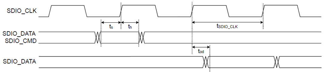
HSPI Secondary
Low Speed Mode
HSPI Secondary Low Speed Mode
| Parameter | Symbol | Test Condition | Min | Typ | Max | Unit |
|---|---|---|---|---|---|---|
| HSPI_CLK | fhspi | 0 | — | 25 | MHz | |
| HSPI_CSN to output delay | tcs | — | — | 7.5 | ns | |
| HSPI_CSN to input setup time | tcst | 4.5 | — | — | ns | |
| HSPI_MOSI, input setup time | ts | 1.4 | — | — | ns | |
| HSPI_MOSI, input hold time | th | 1.5 | — | — | ns | |
| HSPI_MISO, clock to output delay | tod | — | — | 8.75 | ns | |
| Output Load | CL | 5 | — | 10 | pF |
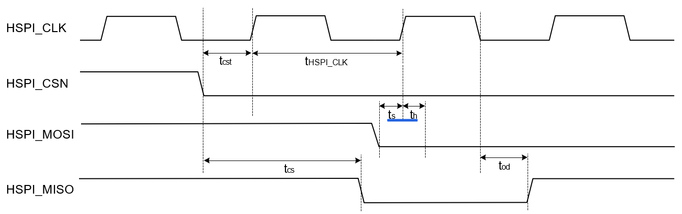
In low speed mode, HSPI_MISO data is driven on the falling edge of HSPI_CLK, and HSPI_MOSI is read on the rising edge of HSPI_CLK.
High Speed Mode
HSPI Secondary High Speed Mode
| Parameter | Symbol | Test Condition | Min | Typ | Max | Unit |
|---|---|---|---|---|---|---|
| HSPI_CLK | fhspi | 25 | — | 80 | MHz | |
| HSPI_CSN to output delay | tcs | — | — | 7.5 | ns | |
| HSPI_CSN to input setup time | tcst | 4.5 | — | — | ns | |
| HSPI_MOSI, input setup time | ts | 1.4 | — | — | ns | |
| HSPI_MOSI, input hold time | th | 1.4 | — | — | ns | |
| HSPI_MISO, clock to output delay | tod | 1.5 | — | 8.75 | ns | |
| Output Load | CL | 5 | — | 10 | pF |
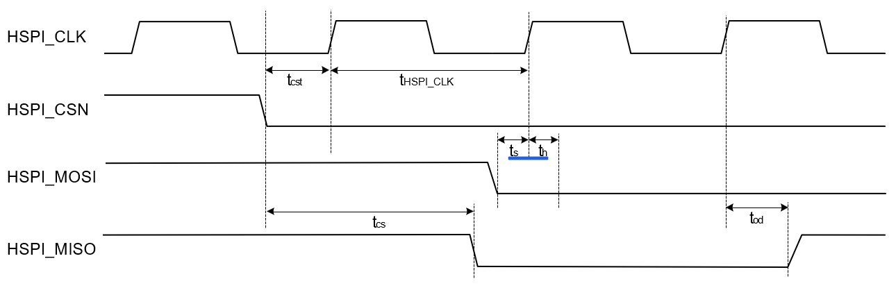
In high speed mode, HSPI_MISO data is driven on the rising edge of HSPI_CLK, and HSPI_MOSI is read on the rising edge of HSPI_CLK.
Ultra High Speed Mode
HSPI Secondary Ultra High Speed Mode
| Parameter | Symbol | Test Condition | Min | Typ | Max | Unit |
|---|---|---|---|---|---|---|
| HSPI_CLK | fhspi | 80 | — | 100 | MHz | |
| HSPI_MOSI, input setup time | ts | 1.4 | — | — | ns | |
| HSPI_MOSI, input hold time | th | 1.4 | — | — | ns | |
| HSPI_MISO, clock to output delay | tod | 1.5 | — | 8.75 | ns | |
| Output Load | CL | 5 | — | 10 | pF |
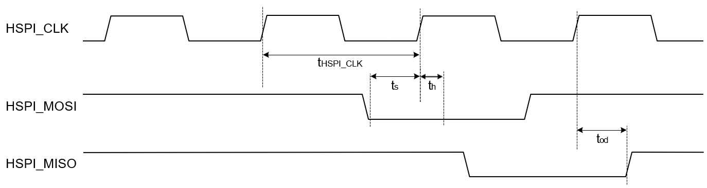
In ultra high speed mode, HSPI_MISO data is driven on the rising edge of HSPI_CLK, and HSPI_MOSI is read on the rising edge of HSPI_CLK.
GPIO Pins
GPIO Pins
| Parameter | Symbol | Test Condition | Min | Typ | Max | Unit |
|---|---|---|---|---|---|---|
| Rise time | trf | Pin configured as output | 1 | — | 5 | ns |
| Fall time | tff | Pin configured as output | 0.9 | — | 5 | ns |
| Rise time | tr | Pin configured as input | 0.3 | — | 1.3 | ns |
| Fall time | tf | Pin configured as input | 0.2 | — | 1.2 | ns |
In-Package Flash Memory
In-Package Flash Memory
| Parameter | Symbol | Test Condition | Min | Typ | Max | Unit |
|---|---|---|---|---|---|---|
| Endurance | Nendu | Sector erase/program | 10000 | — | — | cycles |
| Page erase/program, page in large sector | 10000 | — | — | cycles | ||
| Page erase/program, page in small sector | 10000 | — | — | cycles | ||
| Retention time | tret | Powered | 10 | — | — | years |
| Unpowered | 10 | — | — | years | ||
| Block Erase time (32 KB) | ter | Page, sector or multiple consecutive sectors | — | 150 | 1400 | ms |
| Page programming time | tprog | — | 0.5 | 3 | ms | |
| Chip Erase time | tce | — | 20 | 65 | s |
QSPI
Full Speed Mode (Rising Edge Sampling)
QSPI Full Speed Mode (Rising Edge Sampling)
| Parameter | Symbol | Test Condition | Min | Typ | Max | Unit |
|---|---|---|---|---|---|---|
| qspi_clk | fqspi | 0 | — | 40 | MHz | |
| qspi_cs, to clock edge(this is achieved functionally) | tcs | 8.6 | — | — | ns | |
| qspi_miso, setup time | ts | 4 | — | — | ns | |
| qspi_miso, hold time | th | 2.5 | — | — | ns | |
| qspi_mosi, clock to output valid | tod | -2 | — | 2 | ns | |
| Output Load | CL | 5 | — | 10 | pF |
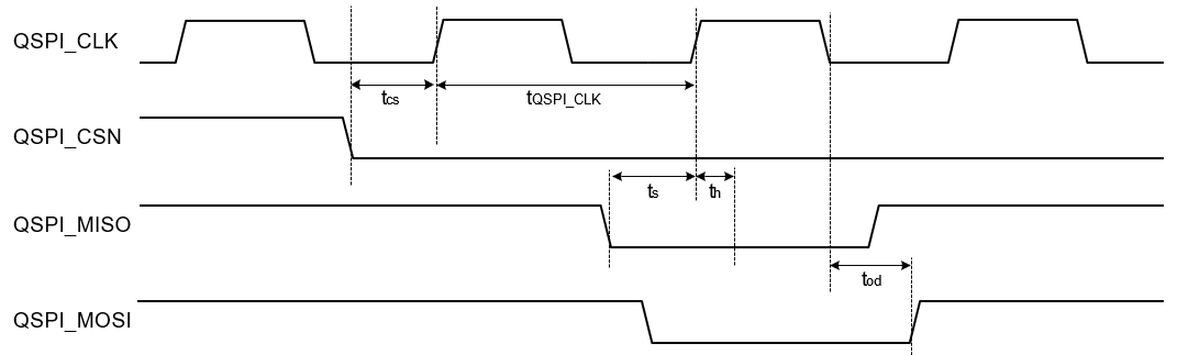
High Speed Mode (Falling Edge Sampling)
QSPI High Speed Mode (Falling Edge Sampling)
| Parameter | Symbol | Test Condition | Min | Typ | Max | Unit |
|---|---|---|---|---|---|---|
| qspi_clk | fqspi | 40 | — | 80 | MHz | |
| qspi_cs, to clock edge (this is achieved functionally) | tcs | 4.3 | — | — | ns | |
| qspi_miso, setup time | ts | 4 | — | — | ns | |
| qspi_miso, hold time | th | 2.5 | — | — | ns | |
| qspi_mosi, clock to output valid | tod | -2 | — | 2 | ns | |
| Output Load | CL | 5 | — | 10 | pF |

PSRAM
Full Speed Mode (Rising Edge Sampling)
PSRAM Full Speed Mode (Rising Edge Sampling)
| Parameter | Symbol | Test Condition | Min | Typ | Max | Unit |
|---|---|---|---|---|---|---|
| psram_clk | fpsram | 0 | — | 40 | MHz | |
| psram_cs, to clock edge (this is achieved functionally) | tcs | 8.6 | — | — | ns | |
| psram_miso, setup time | ts | 4 | — | — | ns | |
| psram_miso, hold time | th | 2.5 | — | — | ns | |
| psram_mosi, clock to output valid | tod | -2 | — | 2 | ns | |
| Output Load | CL | 5 | — | 10 | pF |
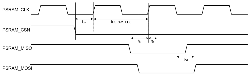
High Speed Mode (Falling Edge Sampling)
PSRAM High Speed Mode (Falling Edge Sampling)
| Parameter | Symbol | Test Condition | Min | Typ | Max | Unit |
|---|---|---|---|---|---|---|
| psram_clk | fpsram | 40 | — | 80 | MHz | |
| psram_cs, to clock edge (this is achieved functionally) | tcs | 4.3 | — | — | ns | |
| psram_miso, setup time | ts | 4 | — | — | ns | |
| psram_miso, hold time | th | 2.5 | — | — | ns | |
| psram_mosi, clock to output valid | tod | -2 | — | 2 | ns | |
| Output Load | CL | 5 | — | 10 | pF |
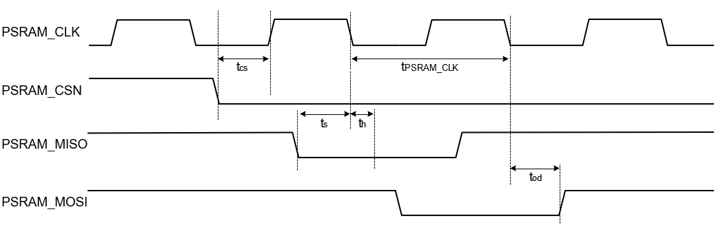
I2C
Fast Speed Mode
I2C Fast Speed Mode
| Parameter | Symbol | Test Condition | Min | Typ | Max | Unit |
|---|---|---|---|---|---|---|
| SCL | fi2c | 100 | — | 400 | kHz | |
| clock low period | tlow | 1.3 | — | — | µs | |
| clock high period | thigh | 0.6 | — | — | µs | |
| start condition, setup time | tsstart | 0.6 | — | — | µs | |
| start condition, hold time | thstart | 0.6 | — | — | µs | |
| data, setup time | ts | 100 | — | — | ns | |
| stop condition, setup time | tsstop | 0.6 | — | — | µs | |
| Output Load | CL | 5 | — | 10 | pF |
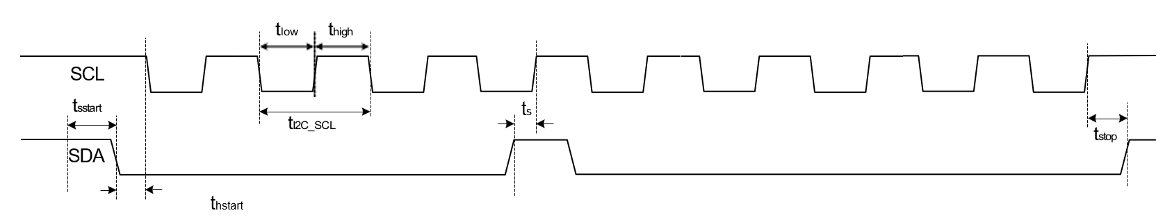
High Speed Mode
I2C High Speed Mode
| Parameter | Symbol | Test Condition | Min | Typ | Max | Unit |
|---|---|---|---|---|---|---|
| SCL | fi2c | 0.4 | — | 3.4 | MHz | |
| clock low period | tlow | 160 | — | — | ns | |
| clock high period | thigh | 60 | — | — | ns | |
| start condition, setup time | tsstart | 160 | — | — | ns | |
| start condition, hold time | thstart | 160 | — | — | ns | |
| data, setup time | ts | 10 | — | — | ns | |
| data, hold time | th | 0 | — | 70 | ns | |
| stop condition, setup time | tsstop | 160 | — | — | ns | |
| Output Load | CL | 5 | — | 10 | pF |
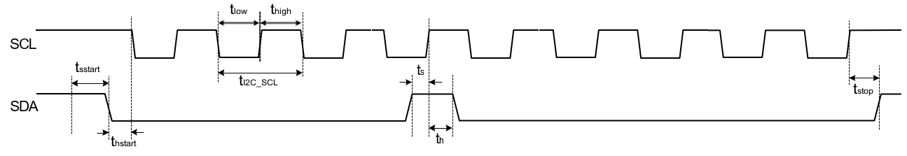
I2S/PCM Primary and Secondary
Primary Mode
Negedge driving and posedge sampling for I2S
Posedge driving and negedge sampling for PCM
I2S/PCM Primary Mode
| Parameter | Symbol | Test Condition | Min | Typ | Max | Unit |
|---|---|---|---|---|---|---|
| i2s_clk | fi2s | 0 | — | 25 | MHz | |
| i2s_din,i2s_ws setup time | ts | 10 | — | — | ns | |
| i2s_din,i2s_ws hold time | th | 3 | — | — | ns | |
| i2s_dout output delay | tod | 0 | — | 15 | ns | |
| i2s_dout output load | CL | 5 | — | 10 | pF |
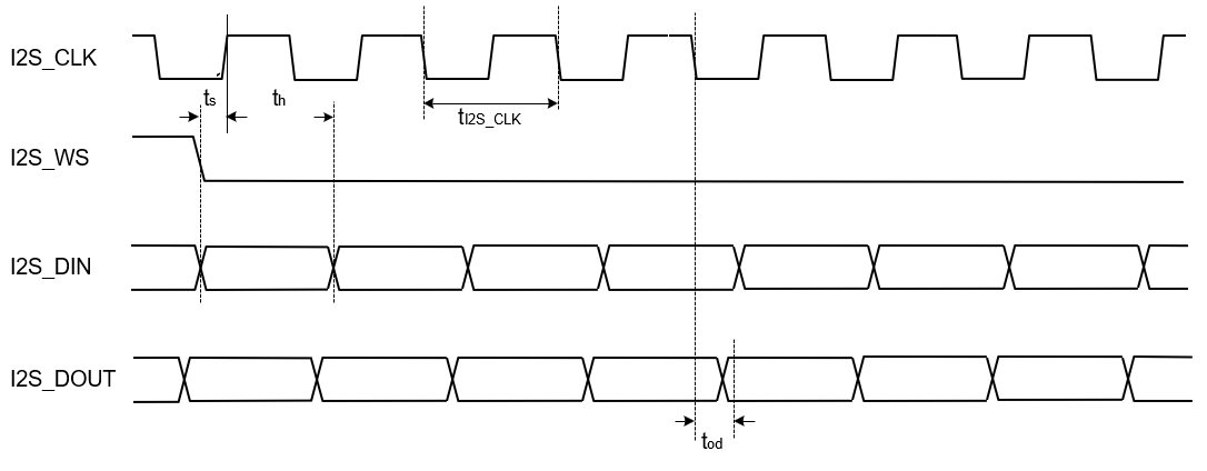
Secondary Mode
Negedge driving and posedge sampling for I2S
Posedge driving and negedge sampling for PCM
I2S/PCM Secondary Mode
| Parameter | Symbol | Test Condition | Min | Typ | Max | Unit |
|---|---|---|---|---|---|---|
| i2s_clk | fi2s | 0 | — | 25 | MHz | |
| i2s_din,i2s_ws setup time | ts | 7.5 | — | — | ns | |
| i2s_din,i2s_ws hold time | th | 2 | — | — | ns | |
| i2s_dout output delay | tod | 0 | — | 17 | ns | |
| i2s_dout output load | CL | 5 | — | 10 | pF |
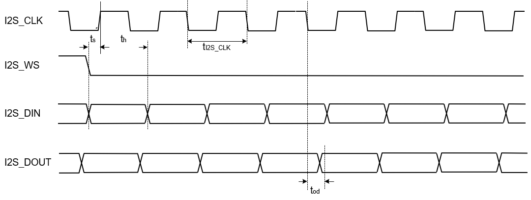
ULP I2S/PCM Primary and Secondary
Primary Mode
Negedge driving and posedge sampling for I2S
Posedge driving and negedge sampling for PCM
ULP I2S/PCM Primary Mode
| Parameter | Symbol | Test Condition | Min | Typ | Max | Unit |
|---|---|---|---|---|---|---|
| i2s_clk | fi2s | 0 | — | 10 | MHz | |
| i2s_din,i2s_ws setup time w.r.t negedge | ts | 15 | — | — | ns | |
| i2s_din,i2s_ws hold time w.r.t negedge | th | 0 | — | — | ns | |
| i2s_dout output delay | tod | 0 | — | 20 | ns | |
| i2s_dout output load | CL | 5 | — | 10 | pF |
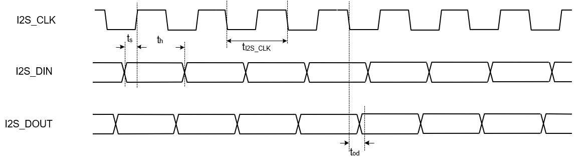
Secondary Mode
Negedge driving and posedge sampling for I2S
Posedge driving and negedge sampling for PCM
ULP I2S/PCM Secondary Mode
| Parameter | Symbol | Test Condition | Min | Typ | Max | Unit |
|---|---|---|---|---|---|---|
| i2s_clk | fi2s | 0 | — | 10 | MHz | |
| i2s_din,i2s_ws setup time w.r.t negedge | ts | 10 | — | — | ns | |
| i2s_din,i2s_ws hold time w.r.t negedge | th | 3 | — | — | ns | |
| i2s_dout output delay | tod | 0 | — | 20 | ns | |
| i2s_dout output load | CL | 5 | — | 10 | pF |
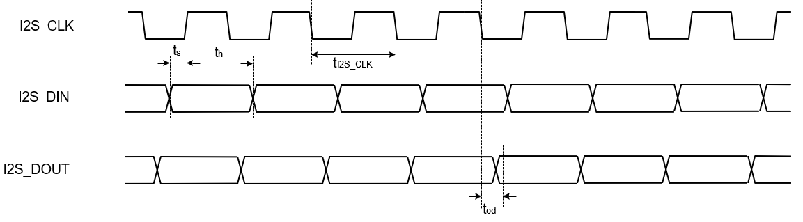
SSI Primary/Secondary
Primary Full Speed Mode
Negedge driving and posedge sampling
SSI Primary Full Speed Mode
| Parameter | Symbol | Test Condition | Min | Typ | Max | Unit |
|---|---|---|---|---|---|---|
| SSI_CLK | fssi | 0 | — | 20 | MHz | |
| SSI_MISO, input setup time | ts | 17 | — | — | ns | |
| SSI_MISO, input hold time | th | 2 | — | — | ns | |
| SSI_CS, SSI_MOSI, clock to output valid | tod | 0 | — | 16 | ns | |
| Output Load | CL | 5 | — | 10 | pF |
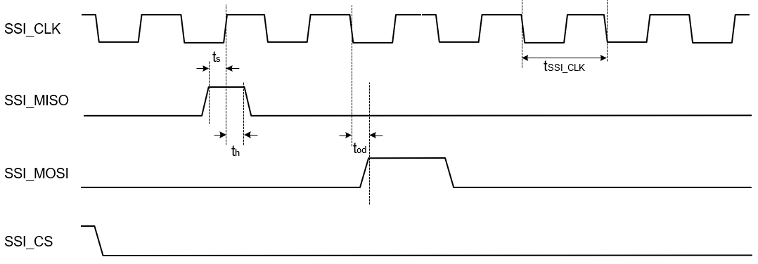
Primary High Speed Mode
SSI Primary High Speed Mode
| Parameter | Symbol | Test Condition | Min | Typ | Max | Unit |
|---|---|---|---|---|---|---|
| SSI_CLK | fssi | 20 | — | 40 | MHz | |
| SSI_MISO, input setup time | ts | 17 | — | — | ns | |
| SSI_MISO, input hold time | th | 2 | — | — | ns | |
| SSI_CS,SSI_MOSI, clock to output valid | tod | 1 | — | 16 | ns | |
| Output Load | CL | 5 | — | 10 | pF |
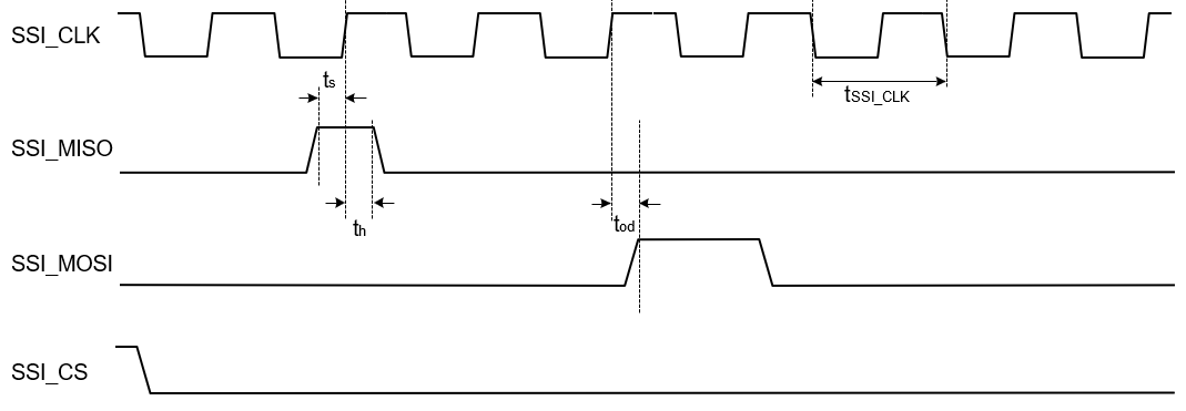
Secondary Full Speed Mode
Negedge driving and posedge sampling
SSI Secondary Full Speed Mode
| Parameter | Symbol | Test Condition | Min | Typ | Max | Unit |
|---|---|---|---|---|---|---|
| SSI_CLK | fssi | 0 | — | 20 | MHz | |
| SSI_MOSI,CS, input setup time | ts | 5 | — | — | ns | |
| SSI_MOSI, input hold time | th | 0 | — | — | ns | |
| SSI_MISO, clock to output delay | tod | — | — | 24 | ns | |
| Output Load | CL | 5 | — | 10 | pF |

ULP SSI Primary
Primary Full Speed Mode
Negedge driving and posedge sampling
ULP SSI Primary Full Speed Mode
| Parameter | Symbol | Test Condition | Min | Typ | Max | Unit |
|---|---|---|---|---|---|---|
| SSI_CLK | fssi | 0 | — | 10 | MHz | |
| SSI_MISO, input setup time | ts | 20 | — | — | ns | |
| SSI_MISO, input hold time | th | 0 | — | — | ns | |
| SSI_CS, SSI_MOSI, clock to output valid | tod | 0 | — | 25 | ns | |
| Output Load | CL | 5 | — | 10 | pF |
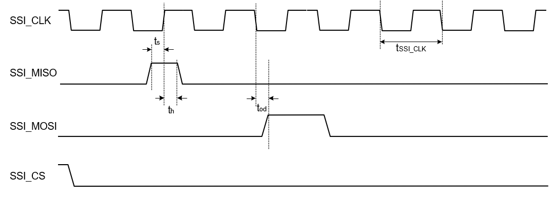
GSPI Primary
Full Speed Mode
GSPI Primary Full Speed Mode
| Parameter | Symbol | Test Condition | Min | Typ | Max | Unit |
|---|---|---|---|---|---|---|
| gspi_clk | fgspi | 0 | — | 58 | MHz | |
| gspi_csn, to clock edge (this is achieved functionally) | tcs | 4.16 | — | — | ns | |
| gspi_miso, setup time | ts | 2 | — | — | ns | |
| gspi_miso, hold time | th | 2 | — | — | ns | |
| gspi_csn, gspi_mosi, clock to output valid | tod | 0 | — | 8 | ns | |
| Output Load | CL | 5 | — | 10 | pF |
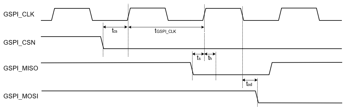
High Speed Mode
GSPI Primary High Speed Mode
| Parameter | Symbol | Test Condition | Min | Typ | Max | Unit |
|---|---|---|---|---|---|---|
| gspi_clk | fgspi | 58 | — | 116 | MHz | |
| gspi_csn, to clock edge (this is achieved functionally) | tcs | 4.16 | — | — | ns | |
| gspi_miso, setup time | ts | 2 | — | — | ns | |
| gspi_miso, hold time | th | 2 | — | — | ns | |
| gspi_csn, gspi_mosi, clock to output valid | tod | 0 | — | 8 | ns | |
| Output Load | CL | 5 | — | 10 | pF |
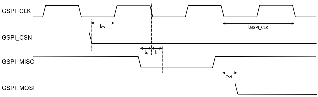
Cortex-M4 JTAG
Cortex-M4F JTAG
| Parameter | Symbol | Test Condition | Min | Typ | Max | Unit |
|---|---|---|---|---|---|---|
| TCK period | ftck | — | — | 20 | MHz | |
| Setup | ts | 5 | — | — | ns | |
| Hold | th | 4 | — | — | ns | |
| Output Delay | tod | 0 | — | 38.5 | ns | |
| Output Load | CL | 5 | — | 10 | pF |
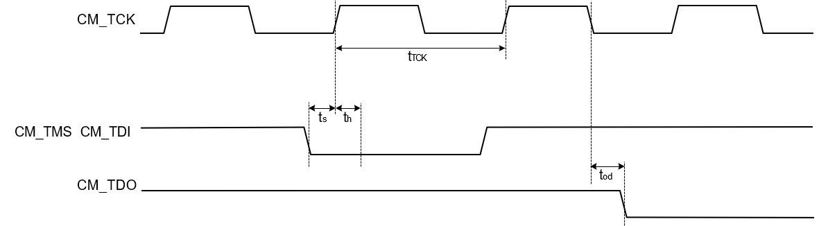
Cortex-M4 Trace
Cortex-M4F Trace
| Parameter | Symbol | Test Condition | Min | Typ | Max | Unit |
|---|---|---|---|---|---|---|
| TRACECLK Period | ftrace | 0 | — | 100 | MHz | |
| Output Delay | tod | 1.2 | — | 8 | ns | |
| Output Load | CL | 5 | — | 10 | pF |
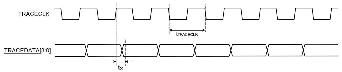
Analog Peripherals
The following analog peripherals are available:
- 2x Analog Comparators
- 3x General purpose Op-Amp
- 16 channel, 12 bit, 5 Msps Analog to Digital Converter with both single ended and differential modes
- 10 bit, 5 MSPS Digital to Analog Converter
Analog Comparators
Analog comparator is a peripheral circuit that compares two analog voltage inputs and gives a logical output based on comparison. There are 9 different inputs for each pin of comparator, and 2 of the 9 are external pin inputs.
The following cases of comparison are possible
- Compare external pin inputs
- Compare external pin input to internal voltages.
- Compare internal voltages.
The comparator compares inputs p and n to produce an output, cmp_out. p > n, cmp_out = 1
p < n, cmp_out = 0
Analog Peripherals consists of 2 comparators whose inputs can be programmed independently. The reference buffer and resistor bank are shared between the two comparators and can be enabled only when at least one of the comparators is enabled.
Analog Comparator Electrical Specifications
| Parameter | Symbol | Test Condition | Min | Typ | Max | Units |
|---|---|---|---|---|---|---|
| Programmable voltage reference range | Vref | 0.1 | 1.1 | V | ||
| Programmable voltage reference step size | Vref_step | 0.1 | V | |||
| The minimum voltage difference required between inputs to make output high | Vos_comp | Typical value corresponds to 1-sigma variation | 1.4 | mV | ||
| Hysteresis = 2'd1 | Vhyst_comp | 60 | mV | |||
| Hysteresis = 2'd3 | 90 | mV | ||||
| Input common-mode range | ICMRcomp | 0.15 | ULP_IO_ VDD - 0.15 | V | ||
| Current consumption on VBATT with all blocks enabled | Iq_comp | 305 | uA |
Auxiliary LDO Electrical Specifications - Regulation Mode
AUX LDO Electrical Specifications - Regulation Mode
| Parameter | Symbol | Test Condition | Min | Typ | Max | Units |
|---|---|---|---|---|---|---|
| Input Supply Voltage | Vin | AUX LDO in Regulation Mode | 2.97 | 3.3 | 3.63 | V |
| Max Output voltage programmable | Voutmax | 2.8 | V | |||
| Min Output voltage programmable | Voutmin | 1.6 | V | |||
| Output voltage programmable step size | Vstep | 80 | mV | |||
| Load current capability | Iload | 16 | mA | |||
| Quiescent current | Iq | 80 | µA |
AUX LDO Electrical Specifications - Bypass Mode
AUX LDO Electrical Specifications - Bypass Mode
| Parameter | Symbol | Test Condition | Min | Typ | Max | Unit |
|---|---|---|---|---|---|---|
| Input Supply Voltage | Vin | AUX LDO in Bypass Mode | 1.71 | 1.8 | 1.98 | V |
| ON Resistance between Vin to Vout pins of AUX LDO | Ron | — | 6.3 | — | Ω | |
| Voltage drop from Vin to Vout | Vdrop | Load = 16 mA (Max) | — | 100 | — | mV |
| Output voltage at AUX_AVDD 1 | Vout | Load = 16 mA at Vin = 1.71 V 2 3 | — | 1.63 | — | V |
Note:
- Vout = Vin - Ron * Iload
- Maximum load current is possible when the three op-amps, two analog comparators, ADC, and DAC are all enabled.
- Programmable output voltage step, Vstep, can vary up to ±5%.
3.1.1 Analog to Digital Converter
- 12 bit precision ADC
- Single ended mode and differential mode configuration
- Two clock latency
ADC Electrical Specifications
| Parameter | Symbol | Test Condition | Min | Typ | Max | Unit |
|---|---|---|---|---|---|---|
| Resolution of ADC | N | — | 12 | — | bits | |
| Number of channels | Nchannel | Single ended Mode | — | 18 | — | channel |
| Differential Mode | — | 9 | — | channel | ||
| ADC sampling and input clock frequency | fADC | — | — | 5 | MHz | |
| Input voltage range | VAIN | Single ended Mode, Positive terminal | 0 | — | AUX_AVDD | V |
| Differential Mode, Positive and negative terminals | 0 | — | AUX_AVDD / 2 | V | ||
| Input resistance | Rin | Single Channel input conversion | — | 100 | — | kΩ |
| ADC internal sample and hold capacitor | Csampled | — | 3 | — | pF | |
| Fixed capacitance from mul- tiplexers and ESD protection | Cfixed | — | 2 | — | pF | |
| Sampling time | ts | 0.1 | — | — | uS | |
| Gain Error | Gerr | -2 | — | 2 | % | |
| Offset | Offset | -2 | — | 2 | mV | |
| Effective number of bits | ENOB | — | 10.1 | — | bits | |
| Signal to noise and distortion ratio | SNDR | — | 62.5 | — | dB | |
| Active current consumption | Iactive | Input frequency 100 kHz at 2.5 Msps | — | 1.5 | — | mA |
Digital to Analog Convertor
- 10 bit precision DAC
- Single ended voltage outputs
- 1.71 to 3.63 V supply operation.
DAC Electrical Specifications
| Parameter | Symbol | Test Condition | Min | Typ | Max | Unit |
|---|---|---|---|---|---|---|
| Lowest output voltage | VOL | — | 0.15 * AUX_AVDD | — | V | |
| Highest output voltage | VOH | — | 0.85 * AUX_AVDD | — | V | |
| Resistive load | Rload | Connect to ground | 5 | — | — | kΩ |
| Load capacitance | Cload | — | — | 50 | pF | |
| Signal to noise and distortion ratio | SNDR | 100 kHz sine wave output and sampling frequency of 5 MHz | — | 50 | — | dB |
| Effective number of bits | ENOB | 100 kHz sine wave output and sampling frequency of 5 MHz | — | 8 | — | bits |
Op-Amp
There are 3 general purpose Operational Amplifiers (Op-Amps) offering rail-to-rail inputs and outputs. The Op-Amps can be configured as:
- Unity gain amplifier
- Trans-Impedance Amplifier (TIA)
- Non-inverting Programmable Gain Amplifier (PGA)
- Inverting Programmable Gain Amplifier (PGA)
- Non-inverting Programmable hysteresis comparator
- Inverting Programmable hysteresis comparator
- Cascaded Non-Inverting PGA
- Cascaded Inverting PGA
- Two Op-Amps Differential Amplifier
- 10. Instrumentation Amplifier
Note:
- In the above list, #7, #8, #9 are configured by cascading 2 Op-Amps
- In the above list, #10 is configured by cascading 3 Op-Amps
Opamp Electrical Specifications
| Parameter | Symbol | Test Condition | Min | Typ | Max | Unit |
|---|---|---|---|---|---|---|
| Input Voltage range | Vin | 0 | — | AUX_AVDD | V | |
| output voltage range | Vout | source or sink 1 mA | 0.1 | — | AUX_AVDD - 0.1 | V |
| output current capability, source or sink | Iout | 0.5 < Vout < AUX_AVDD-0.5 | — | — | 3 | mA |
| Input offset voltage (1 sigma) | Vos | Power mode = high, CL = 50 pF | — | 2.2 | — | mV |
| Power mode = low, CL = 50 pF | — | 2.2 | — | mV | ||
| Gain error, unity gain buffer mode, RL = 1 kΩ | Ge1 | Power mode = high, CL = 50 pF | — | 1 | — | % |
| Power mode = low, CL = 50 pF | — | 1 | — | % | ||
| Phase margin, in UGB mode | PM | Power mode = high, CL = 50 pF | — | 59 | — | °C |
| Power mode = low, CL = 50 pF | — | 63 | — | °C | ||
| Gain-bandwidth product | GBW | Power mode = high, CL = 50 pF | — | 17 | — | MHz |
| Power mode = low, CL = 50 pF | — | 7.5 | — | MHz | ||
| Total Harmonic Distortion, at 100 kHz (UGB mode) | THDUGB | Power mode = high, CL = 50 pF | — | -64 | — | dB |
| Power mode = low, CL = 50 pF | — | -62 | — | dB | ||
| Total Harmonic Distortion, at 10 kHz (Non inv amp mode, gain = 51) | THD | Power mode = high, CL = 50 pF | — | -58 | — | dB |
| Power mode = low, CL = 50 pF | — | -56 | — | dB | ||
| DC Power supply rejection ratio | PSRR | Power mode = high, CL = 50 pF | — | 90 | — | dB |
| Power mode = low, CL = 50 pF | — | 90 | — | dB | ||
| DC Common mode rejection ratio | CMRR | Power mode = high, CL = 50 pF | — | 70 | — | dB |
| Power mode = low, CL = 50 pF | — | 71 | — | dB | ||
| Quiescent current - 1 Op- Amp | Idd | Power mode = high, CL = 50 pF | — | 0.95 | — | mA |
| Power mode = low, CL = 50 pF | — | 315 | — | µA |
Temperature Sensor
- Generates PTAT Voltage from BJT based band gap.
- Buffered PTAT voltage is given at ADC Input.
- Output of the ADC is linear function of temperature.
The BJT based sensor works over the full operating temperature and supply range of the device. It outputs a digital word having a resolution of nearly 1 ºC. The conversion time is 2 clock cycles of ADC after turning ON the temperature sensor. Typically, the block consumes 110 uA of current and leakage current is 800 pA.
BJT Based Temperature Sensor Electrical Specifications
| Parameter | Symbol | Test Condition | Min | Typ | Max | Unit |
|---|---|---|---|---|---|---|
| Accuracy | Tacc | — | 5 | — | °C |
MCU Current Consumption
MCU Power State Current Consumption
TA = 25 °C. VBATT = 3.3 V. Remaining supplies are at typical operating conditions. All numbers taken with NWP in shutdown mode.
MCU Power State Current Consumption
| Parameter | Symbol | Test Condition | Min | Typ | Max | Unit |
|---|---|---|---|---|---|---|
| PS4 Supply Current | IPS4 | Sleep, 320 KB RAM retained, SRAM PERI ON, SCDC = 1.05 V, Ret LDO = 0.75 V | — | 12.9 | — | µA |
| Active - Default configuration | — | 8.8 | — | mA | ||
| PS3 Supply Current | IPS3 | Sleep, 320 KB RAM retained, SRAM PERI ON, SCDC = 1.05 V, Ret LDO = 0.75 V | — | 12.9 | — | µA |
| Active - Default configuration | — | 5.9 | — | mA | ||
| PS2 Supply Current | IPS2 | Sleep, 320 KB RAM retained, SRAM PERI ON, SCDC = 1.05 V, Ret LDO = 0.75 V | — | 12.9 | — | µA |
| Active - Default configuration | — | 815 | — | µA | ||
| PS1 Supply Current | IPS1 | Sleep, 320 KB RAM retained, SRAM PERI ON, SCDC = 1.05 V, Ret LDO = 0.75 V | — | 12.9 | — | µA |
| PS0 Supply Current | IPS0 | Sleep, 320 KB RAM retained, SRAM PERI ON, SCDC = 1.05 V, Ret LDO = 0.75 V | — | 12.9 | — | µA |
| Sleep, without RAM retention, SRAM PERI ON, SCDC = 1.05 V, Ret LDO = 0.75 V | — | 1.3 | — | µA |
Radio Characteristics
In the sub-sections below,
- All numbers are measured at TA = 25°C, VBATT = 3.3 V
- Please refer to Reference Schematics, BOM, and Layout Guidelines. The integrated RF front end includes the matching network, RF switch, and a band-pass filter.
Supported WLAN channels for different regions include:
- US: Channels 1 (2412 MHz) through 11 (2462 MHz)
- Europe: Channels 1 (2412 MHz) through 13 (2472 MHz)
- Japan: Channels 1 (2412 MHz) through 14 (2484 MHz), Channel 14 supports 1 and 2 Mbps data rates only
WLAN 2.4 GHz Radio Receiver Characteristics
WLAN 2.4 GHz Receiver Characteristics on High-Performance (HP) Mode
Unless otherwise indicated, typical conditions are: TA = 25 °C. VBATT = 3.3 V. Remaining supplies are at typical operating conditions. Parameters are referred at antenna port.
WLAN 2.4 GHz Receiver Characteristics on HP Mode
| Parameter | Symbol | Test Condition | Min | Typ | Max | Unit |
|---|---|---|---|---|---|---|
| Sensitivity for 20 MHz Bandwidth 1, 2 | SENS | 802.11b 1 Mbps DSSS 3 | — | -95 | — | dBm |
| 802.11b 11 Mbps CCK 3 | — | -86 | — | dBm | ||
| 802.11g 6 Mbps OFDM 4 | — | -90.5 | — | dBm | ||
| 802.11g 54 Mbps OFDM 4 | — | -74 | — | dBm | ||
| 802.11n HT20 MCS0 Mixed Mode | — | -89.5 | — | dBm | ||
| 802.11n HT20 MCS7 Mixed Mode | — | -69.5 | — | dBm | ||
| 802.11ax HE20 MCS0 SU 6 | — | -89 | — | dBm | ||
| 802.11ax HE20 MCS7 SU 6 | — | -68.5 | — | dBm | ||
| 802.11ax HE20 MCS0 ER 6 | — | -91 | — | dBm | ||
| Maximum Input Level for PER below 10% | RXSAT | 802.11b | — | 5 | — | dBm |
| 802.11g | — | 0 | — | dBm | ||
| 802.11n | — | 0 | — | dBm | ||
| 802.11ax | — | 0 | — | dBm | ||
| RSSI Accuracy Range | RSSIRNG | — | +4/-5 | — | dB | |
| Adjacent Channel Interference 7 | ACI | 802.11b 1 Mbps DSSS 3 8 | — | 51 | — | dB |
| 802.11b 11 Mbps CCK 3 8 | — | 34 | — | dB | ||
| 802.11g 6 Mbps OFDM 4 9 | — | 43 | — | dB | ||
| 802.11g 54 Mbps OFDM 4 9 | — | 26 | — | dB | ||
| 802.11n HT20 MCS0 Mixed Mode | — | 33 | — | dB | ||
| 802.11n HT20 MCS7 Mixed Mode | — | 12 | — | dB | ||
| 802.11ax HE20 MCS0 SU 6 9 | — | 21 | — | dB | ||
| 802.11ax HE20 MCS7 SU 6 9 | — | 6 | — | dB |
Note:
- RX Sensitivity Variation is up to 3 dB for channels (1, 2, 3, 4, 5, 9, and 10) at typical / room temperature.
- RX Sensitivity may be degraded up to 4 dB for channels (6, 7, 8, 11, 12, 13 and 14) at typical / room temperature.
- 802.11b, Packet size is 1024 bytes, < 8% PER limit, Carrier modulation is non-DCM
- 802.11g, Packet size is 1024 bytes, < 10% PER limit, Carrier modulation is non-DCM
- 802.11n, Packet size is 4096 bytes, < 10% PER limit, Carrier modulation is non-DCM
- 802.11ax, Packet size is 4096 bytes, < 10% PER limit, Carrier modulation is non-DCM
- ACI / AACI is calculated as Interferer Power(dBm)- Inband power(dBm)
- Desired signal power is 6 dB above standard defined sensitivity level
- Desired signal power is 3dB above standard defined sensitivity level
WLAN 2.4 GHz Receiver Characteristics on Low-Power (LP) Mode
Unless otherwise indicated, typical conditions are: TA = 25 °C. VBATT = 3.3 V. Remaining supplies are at typical operating conditions. Parameters are referred at antenna port.
WLAN 2.4 GHz Receiver Characteristics on LP Mode
| Parameter | Symbol | Test Condition | Min | Typ | Max | Unit |
|---|---|---|---|---|---|---|
| Sensitivity for 20 MHz Bandwidth 1 2 | SENS | 802.11b 1 Mbps DSSS 3 | — | -95 | — | dBm |
| 802.11b 11 Mbps CCK 3 | — | -86 | — | dBm | ||
| 802.11g 6 Mbps OFDM 4 | — | -90 | — | dBm | ||
| 802.11g 36 Mbps OFDM 4 | — | -79 | — | dBm | ||
| 802.11n HT20 MCS0 Mixed Mode | — | -88 | — | dBm | ||
| 802.11n HT20 MCS4 Mixed Mode | — | -77 | — | dBm | ||
| Maximum Input Level for PER below 10% | RXSAT | 802.11b | — | -2.5 | — | dBm |
| 802.11g | — | 1.5 | — | dBm | ||
| 802.11n | — | 0.5 | — | dBm | ||
| RSSI Accuracy Range | RSSIRNG | — | +4/-6 | — | dB | |
| Adjacent Channel Interfer- ence 6 | ACI | 802.11b 1 Mbps DSSS 3 7 | — | 52 | — | dB |
| 802.11b 11 Mbps CCK 3 7 | — | 33 | — | dB | ||
| 802.11g 6 Mbps OFDM 4 8 | — | 44 | — | dB | ||
| 802.11g 36 Mbps OFDM 4 8 | — | 29 | — | dB | ||
| 802.11n HT20 MCS0 Mixed Mode | — | 33 | — | dB | ||
| 802.11n HT20 MCS4 Mixed Mode | — | 20 | — | dB | ||
| Alternate Adjacent Channel Interference 6 | AACI | 802.11b 1 Mbps DSSS 3 7 | — | 53 | — | dB |
| 802.11b 11 Mbps CCK 3 7 | — | 37 | — | dB | ||
| 802.11g 6 Mbps OFDM 4 8 | — | 53 | — | dB | ||
| 802.11g 36 Mbps OFDM 4 8 | — | 37 | — | dB | ||
| 802.11n HT20 MCS0 Mixed Mode | — | 52 | — | dB | ||
| 802.11n HT20 MCS4 Mixed Mode | — | 36 | — | dB |
Note:
- RX Sensitivity Variation is up to 3 dB for channels (1, 2, 3, 4, 5, 9, and 10) at typical / room temperature
- RX Sensitivity may be degraded up to 4 dB for channels (6, 7, 8, 11, 12, 13 and 14) at typical / room temperature
- 802.11b, Packet size is 1024 bytes, < 8% PER limit, Carrier modulation is non-DCM
- 802.11g, Packet size is 1024 bytes, < 10% PER limit, Carrier modulation is non-DCM
- 802.11n, Packet size is 4096 bytes, < 10% PER limit, Carrier modulation is non-DCM
- ACI / AACI is calculated as Interferer Power(dBm)- Inband power(dBm)
- Desired signal power is 6 dB above standard defined sensitivity level
- Desired signal power is 3dB above standard defined sensitivity level
WLAN 2.4 GHz Transmitter Characteristics
Transmitter Characteristics with 3.3V Supply
Unless otherwise indicated, typical conditions are: TA = 25°C, VBATT = 3.3V. Remaining supplies are at typical operating conditions. Parameters are referred at antenna port.
| Parameter | Symbol | Test Condition | Min | Typ | Max | Unit |
|---|---|---|---|---|---|---|
| Transmit Power for 20 MHz Bandwidth, with EVM limits 1, 2,5 | POUT | 802.11b 1 Mbps DSSS, EVM< -9 dB | — | 17 | — | dBm |
| 802.11b 11 Mbps CCK, EVM< -9 dB | — | 17 | — | dBm | ||
| 802.11g 6 Mbps OFDM, EVM< -5 dB 3 | — | 17.5 | — | dBm | ||
| 802.11g 54 Mbps OFDM, EVM< -25 dB 3 | — | 13.5 | — | dBm | ||
| 802.11n HT20 MCS0 Mixed Mode, EVM< -5 dB3 | — | 17 | — | dBm | ||
| 802.11n HT20 MCS7 Mixed Mode, EVM< -27 dB3 | — | 12.5 | — | dBm | ||
| 802.11ax HE20 MCS0 SU, EVM< | — | 16 | — | dBm | ||
| 802.11ax HE20 MCS7 SU, EVM< | — | 11 | — | dBm | ||
| Power variation across channels | POUTVAR_CH | — | 2 | — | dB |
Note:
- Transmit power listed in this table is average power across all channels.
- TX power in edge channels will be limited by Restricted band edge in the FCC region.
- 11g/n/ax TX power in edge channels will be limited by Unwanted Emissions in MIC region.
- 11ax TX power will be limited by PSD in the ETSI region.
- Channels 1 (2412MHz) through 11 (2462MHz) are supported for North America (FCC,ISED). Channels 1 (2412MHz) through 13 (2472 MHz) are supported for Europe and Japan (CE, MIC). Channel 14 (2484 MHz) is additionally supported for Japan.
WLAN Current Consumption
The following shows the supply connection and measurement point for supply current numbers in this section. Note that for WLAN and BLE supply current measurements, the MCU is in deep sleep mode with no RAM retained. All measurements are taken on devices with in-package flash. The impact of external SRAM on current consumption is detailed in Flash and PSRAM Supply Connections.

WLAN 2.4 GHz
TA = 25 °C. VBATT = 3.3 V. Remaining supplies are at typical operating conditions. NWP clock running at 80 MHz.
WLAN 2.4 GHz 3.3 V Current Consumption
| Parameter | Symbol | Test Condition | Min | Typ | Max | Unit |
|---|---|---|---|---|---|---|
| Listen current | IRX_LISTEN | LP mode, 1 Mbps Listen | — | 14 | — | mA |
| Active Receive Current | IRX_ACTIVE | 1 Mbps RX Active, LP mode | — | 21 | — | mA |
| HT20 MCS0, HP mode | — | 54 | — | mA | ||
| HT20 MCS7, HP mode | — | 55 | — | mA | ||
| HE20 MCS0, HP mode | — | 55 | — | mA | ||
| HE20 MCS7, HP mode | — | 55 | — | mA | ||
| Transmit Current | ITX | 1 Mbps, HP mode | — | 223 | — | mA |
| HT20 MCS0, HP mode | — | 231 | — | mA | ||
| HT20 MCS7, HP mode | — | 175 | — | mA | ||
| HE20 MCS0, HP mode | — | 212 | — | mA | ||
| HE20 MCS7, HP mode | — | 169 | — | mA | ||
| Deep Sleep | ISLEEP | No RAM retained | — | 5 | — | µA |
| 352 KB RAM retained | — | 12.5 | — | µA | ||
| Standby Associated, DTIM = 10 | ISTBY_ASSOC | WLAN Keep Alive Every 30 s with 352 KB RAM Retained, Without TCP Keep Alive | — | 78 | — | µA |
| 11ax TWT, Auto Config Ena- bled, Without TCP Keep Alive | ISTBY_AX | RX latency 2 s with 8 ms wakeup duration, WLAN Keep Alive Every 30 s with 352 KB RAM Retained | — | 97 | — | µA |
| RX latency 30 s with 8 ms wakeup duration, WLAN Keep Alive Every 30 s with 352 KB RAM Retained | — | 37 | — | µA | ||
| RX latency 60 s with 8 ms wakeup duration, WLAN Keep Alive Every 60 s with 352 KB RAM Retained | — | 27 | — | µA | ||
| 11ax TWT, Auto Config Ena- bled, With TCP Keep Alive Every 240 s | ISTBY_AX_TCP | RX latency 2 s with 8 ms wakeup duration, WLAN Keep Alive Every 30 s with 352 KB RAM Retained | — | 101 | — | µA |
| RX latency 30 s with 8 ms wakeup duration, WLAN Keep Alive Every 30 s with 352 KB RAM Retained | — | 43 | — | µA | ||
| RX latency 60 s with 8 ms wakeup duration, WLAN Keep Alive Every 60 s with 352 KB RAM Retained | — | 32 | — | µA |
Note:
- The absolute maximum device current when transmitting at highest transmit power will not exceed 400 mA.
Bluetooth Receiver Characteristics
Bluetooth Transmitter Characteristics
Bluetooth Transmitter Characteristics on High-Performance (HP) Mode
Unless otherwise indicated, typical conditions are: TA = 25 °C, VBATT = 3.3 V, and remaining supplies are at typical operating conditions. Parameters are referred at antenna port.
Bluetooth Transmitter Characteristics on HP Mode 3.3 V
| Parameter | Symbol | Test Condition | Min | Typ | Max | Unit |
|---|---|---|---|---|---|---|
| Transmit Power 1 2 | POUT | LE 1 Mbps | — | 17 | — | dBm |
| LE 2 Mbps 3 | — | 17 | — | dBm | ||
| LR 500 kbps | — | 17 | — | dBm | ||
| LR 125 kbps | — | 17 | — | dBm | ||
| Power variation across channels | POUTVAR_CH | — | 2 | — | dB | |
| Adjacent Channel Power |M- N| = 2 | ACPeq2 | LE | — | -33 | — | dBm |
| Adjacent Channel Power |M- N| > 2 | ACPgt2 | LE | — | -40 | — | dBm |
| BLE Modulation Characteristics at 1 Mbps | MODCHAR | Δf1 Avg | — | 248 | — | kHz |
| Δf2 Max | — | 250 | — | kHz | ||
| Δf2 Avg/Δf1 Avg | — | 1.43 | — |
Note:
- ETSI Max Power is limited to 10 dBm/MHz EIRP to meet PSD requirements, because device falls under DTS.
- In FCC, LR 125kbps Max Power is limited to 11 dBm to meet PSD requirement, because device falls under DTS.
- In MIC Max power is limited to 7dBm to meet 10 dBm/MHz limit
Bluetooth Transmitter Characteristics on Low-Power (LP) 0 dBm RF Mode
Unless otherwise indicated, typical conditions are: TA = 25 °C, VBATT = 3.3 V, and remaining supplies are at typical operating conditions. Parameters are referred at antenna port.
Bluetooth Transmitter Characteristics on Low-Power (LP) 0 dBm RF Mode
| Parameter | Symbol | Test Condition | Min | Typ | Max | Unit |
|---|---|---|---|---|---|---|
| Transmit Power | POUT | LE 1 Mbps | — | -2 | — | dBm |
| LE 2 Mbps | — | -2 | — | dBm | ||
| LR 500 kbps | — | -2 | — | dBm | ||
| LR 125 kbps | — | -2 | — | dBm | ||
| Adjacent Channel Power |M- N| = 2 | ACPeq2 | LE | — | -42 | — | dBm |
| Adjacent Channel Power |M- N| > 2 | ACPgt2 | LE | — | -51 | — | dBm |
| BLE Modulation Characteristics | MODCHAR | Δf1 Avg | — | 248 | — | kHz |
| Δf2 Max | — | 250 | — | kHz | ||
| Δf2 Avg/Δf1 Avg | — | 1.3 | — | kHz |
Bluetooth Receiver Characteristics for 1 Mbps Data Rate
Unless otherwise indicated, typical conditions are: TA = 25 °C, VBATT = 3.3 V, remaining supplies are at typical operating conditions, packet length is 37 bytes, and parameters are referred at antenna port. Unless otherwise indicated, specifications apply to both HP and LP modes.
Bluetooth Receiver Characteristics for 1 Mbps Data Rate
| Parameter | Symbol | Test Condition | Min | Typ | Max | Unit |
|---|---|---|---|---|---|---|
| Max usable receiver input level | RXSAT | Signal is reference signal, 255 byte payload, BER = 0.017%, HP Mode | — | 5 | — | dBm |
| Signal is reference signal, 255 byte payload, BER = 0.017%, LP Mode | — | 1.5 | — | dBm | ||
| Sensitivity 1 | SENS | Signal is reference signal, 37 byte payload, BER = 0.1% | — | -93 | — | dBm |
| Signal is reference signal, 255 byte payload, BER = 0.017% | — | -91 | — | dBm | ||
| Signal to co-channel interferer 2 | C/ICC | (see notes)3 4 | — | -10 | — | dB |
| N ± 1 Adjacent channel selectivity 2 | C/I1 | Interferer is reference signal at +1 MHz offset3 4 5 6 | — | 4 | — | dB |
| Interferer is reference signal at -1 MHz offset3 4 5 6 | — | -4 | — | dB | ||
| N ± 2 Alternate channel se- lectivity 2 | C/I2 | Interferer is reference signal at +2 MHz offset3 4 5 6 | — | 26 | — | dB |
| Interferer is reference signal at -2 MHz offset3 4 5 6 | — | 23 | — | dB | ||
| N ± 3 Alternate channel se- lectivity 2 | C/I3 | Interferer is reference signal at +3 MHz offset3 4 5 6 | — | 39 | — | dB |
| Interferer is reference signal at -3 MHz offset3 4 5 6 | — | 28 | — | dB | ||
| Selectivity to image frequen- cy 2 | C/IIM | Interferer is reference signal at image frequency3 4 6 | — | 39 | — | dB |
| Selectivity to image frequen- cy ± 1 MHz 2 | C/IIM_1 | Interferer is reference signal at image frequency +1 MHz3 4 6 | — | 39 | — | dB |
| Interferer is reference signal at image frequency -1 MHz3 4 6 | — | 36 | — | dB |
Note:
- There is up to 3 dB sensitivity degradation for channels 18, 35, and 37 .
- C/I is calculated as Interferer Power (dBm) - Inband power (dBm)
- 0.1% BER, 37 byte packet size
- Desired signal = -67 dBm
- Desired frequency 2402 MHz ≤ Fc ≤ 2480 MHz
- Withallowedexceptions
Bluetooth Receiver Characteristics for 2 Mbps Data Rate
Unless otherwise indicated, typical conditions are: TA = 25 °C, VBATT = 3.3 V, remaining supplies are at typical operating conditions, packet length is 37 bytes, and parameters are referred at antenna port. Unless otherwise indicated, specifications apply to both HP and LP modes.
Bluetooth Receiver Characteristics for 2 Mbps Data Rate
| Parameter | Symbol | Test Condition | Min | Typ | Max | Unit |
|---|---|---|---|---|---|---|
| Max usable receiver input level | RXSAT | Signal is reference signal, 255 byte payload, BER = 0.017%, HP mode | — | 0 | — | dBm |
| Signal is reference signal, 255 byte payload, BER = 0.017%, LP mode | — | -2.5 | — | dBm | ||
| Sensitivity | SENS | Signal is reference signal, 37 byte payload, BER = 0.1% | — | -90.5 | — | dBm |
| Signal is reference signal, 255 byte payload, BER = 0.017% | — | -88.5 | — | dBm | ||
| Signal to co-channel interfer- er 1 | C/ICC | (see notes)2 3 | — | -7 | — | dB |
| N ± 1 Adjacent channel se- lectivity 1 | C/I1 | Interferer is reference signal at +2 MHz offset2 4 3 5 | — | 4 | — | dB |
| Interferer is reference signal at -2 MHz offset2 4 3 5 | — | 6 | — | dB | ||
| N ± 2 Alternate channel se- lectivity 1 | C/I2 | Interferer is reference signal at +4 MHz offset2 4 3 5 | — | 22 | — | dB |
| Interferer is reference signal at -4 MHz offset2 4 3 5 | — | 16 | — | dB | ||
| Selectivity to image frequen- cy 1 | C/IIM | Interferer is reference signal at im- age frequency2 3 5 | — | 16 | — | dB |
| Selectivity to image frequen- cy ± 2 MHz 1 | C/IIM_1 | Interferer is reference signal at im- age frequency +2 MHz2 3 5 | — | 37 | — | dB |
| Interferer is reference signal at im- age frequency -2 MHz2 3 5 | — | 28 | — | dB |
Note:
- C/I is calculated as Interferer Power (dBm) - Inband power (dBm)
- 0.1% BER, 37 byte packet size
- Desired signal = -67 dBm
- Desired frequency 2402 MHz ≤ Fc ≤ 2480 MHz
- With allowed exceptions
Bluetooth Receiver Characteristics for 125 kbps Data Rate
Unless otherwise indicated, typical conditions are: TA = 25 °C, VBATT = 3.3 V, remaining supplies are at typical operating conditions, packet length is 37 bytes, and parameters are referred at antenna port. Unless otherwise indicated, specifications apply to both HP and LP modes.
Bluetooth Receiver Characteristics for 125 kbps Data Rate
| Parameter | Symbol | Test Condition | Min | Typ | Max | Unit |
|---|---|---|---|---|---|---|
| Max usable receiver input level | RXSAT | Signal is reference signal, 255 byte payload, BER = 0.017%, HP mode | — | 5 | — | dBm |
| Signal is reference signal, 255 byte payload, BER = 0.017%, LP mode | — | 3.5 | — | dBm | ||
| Sensitivity 1 | SENS | Signal is reference signal, 37 byte payload, BER = 0.1% | — | -104.5 | — | dBm |
| Signal is reference signal, 255 byte payload, BER = 0.017% | — | -103.5 | — | dBm |
Note:
- BLE, LR: Sensitivities for channels 19, 39 are up to 2 dB lower performance
Bluetooth Receiver Characteristics for 500 kbps Data Rate
Unless otherwise indicated, typical conditions are: TA = 25 °C, VBATT = 3.3 V, remaining supplies are at typical operating conditions, packet length is 37 bytes, and parameters are referred at antenna port. Unless otherwise indicated, specifications apply to both HP and LP modes.
Bluetooth Receiver Characteristics for 500 kbps Data Rate
| Parameter | Symbol | Test Condition | Min | Typ | Max | Unit |
|---|---|---|---|---|---|---|
| Max usable receiver input level | RXSAT | Signal is reference signal, 255 byte payload, BER = 0.017%, HP Mode | — | 5 | — | dBm |
| Signal is reference signal, 255 byte payload, BER = 0.017%, LP Mode | — | 3.5 | — | dBm | ||
| Sensitivity 1 | SENS | Signal is reference signal, 37 byte payload, BER = 0.1% | — | -100 | — | dBm |
| Signal is reference signal, 255 byte payload, BER = 0.017% | — | -98.5 | — | dBm |
Bluetooth Current Consumption
The following shows the supply connection and measurement point for supply current numbers in this section. Note that for WLAN and BLE supply current measurements, the MCU is in deep sleep mode with no RAM retained. All measurements are taken on devices with in-package flash. The impact of external SRAM on current consumption is detailed in Flash and PSRAM Supply Connections.
Bluetooth LE
TA = 25 °C. VBATT = 3.3 V. Remaining supplies are at typical operating conditions. NWP clock running at 80 MHz.
Bluetooth LE Current Consumption
| Parameter | Symbol | Test Condition | Min | Typ | Max | Unit |
|---|---|---|---|---|---|---|
| TX Active Current | ITX | LP mode, Tx Power = 0 dBm | — | 11 | — | mA |
| LP mode, Tx Power = Max TX power | — | 11 | — | mA | ||
| RX Active Current | IRX | LP mode | — | 11 | — | mA |
| Advertising, Unconnectable | IADV_UC | Advertising on all 3 channels, 37 Byte payload, Interval = 1.28 s, Tx Power = 0 dBm, LP mode | — | 35 | — | µA |
| Advertising, Connectable | IADV_CN | Advertising on all 3 channels, 37 Byte payload, Interval = 1.28 s, Tx Power = 0 dBm, LP mode | — | 41 | — | µA |
| Connected | ICONN | Connection Interval = 200 ms, No data, Tx Power = 0 dBm, LP mode | — | 138 | — | µA |
Integration Guidelines
Antenna Characteristics
453-00222 Antenna Radiation and Efficiency
Typical radiation patterns for the built-in antenna under optimal operating conditions are plotted in the figures that follow.
Antenna Efficiency and Peak Gain
| Parameter | With optimal layout | Note |
|---|---|---|
| Efficiency | -1 dB | Antenna gain and radiation patterns have a strong dependence on the size and shape of the application PCB the module is mounted on, as well as on the proximity of any mechanical design to the antenna. Refer to 8.3.2 Installation Guide for 453-00222 Module for recommendations to achieve optimal antenna performance. |
| Peak gain | 2.26 dBi |
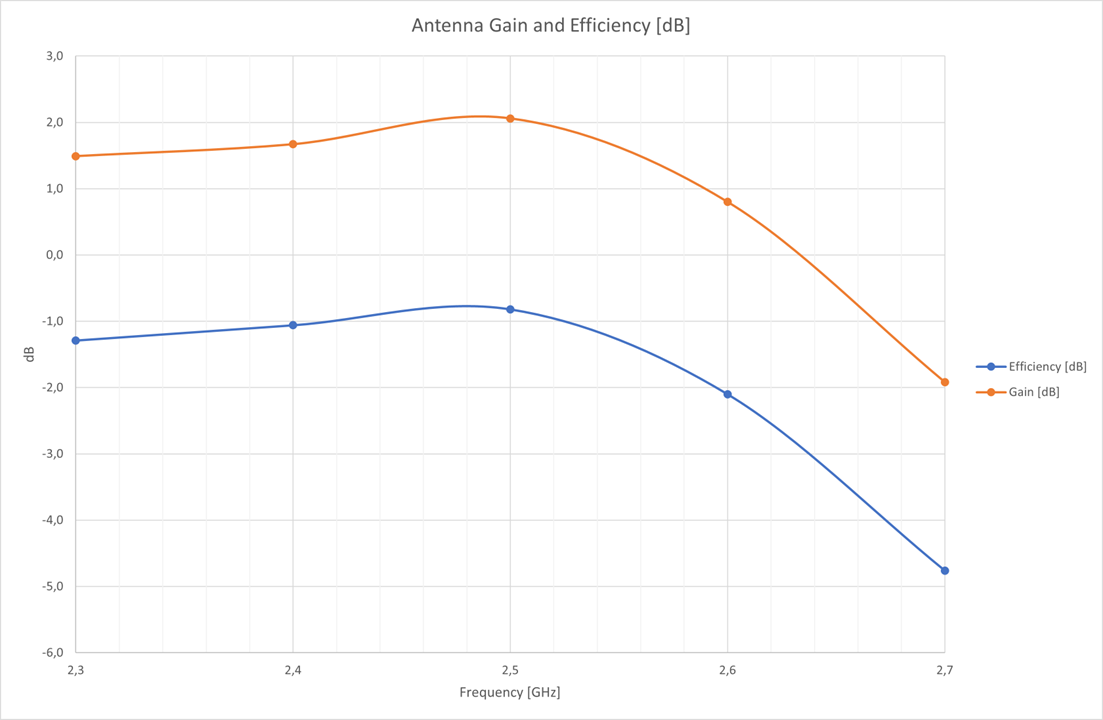
Radiation Patterns
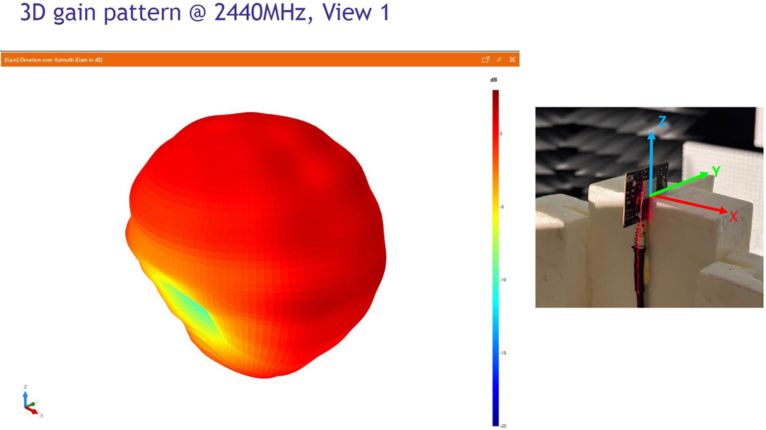
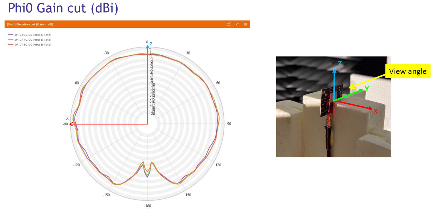

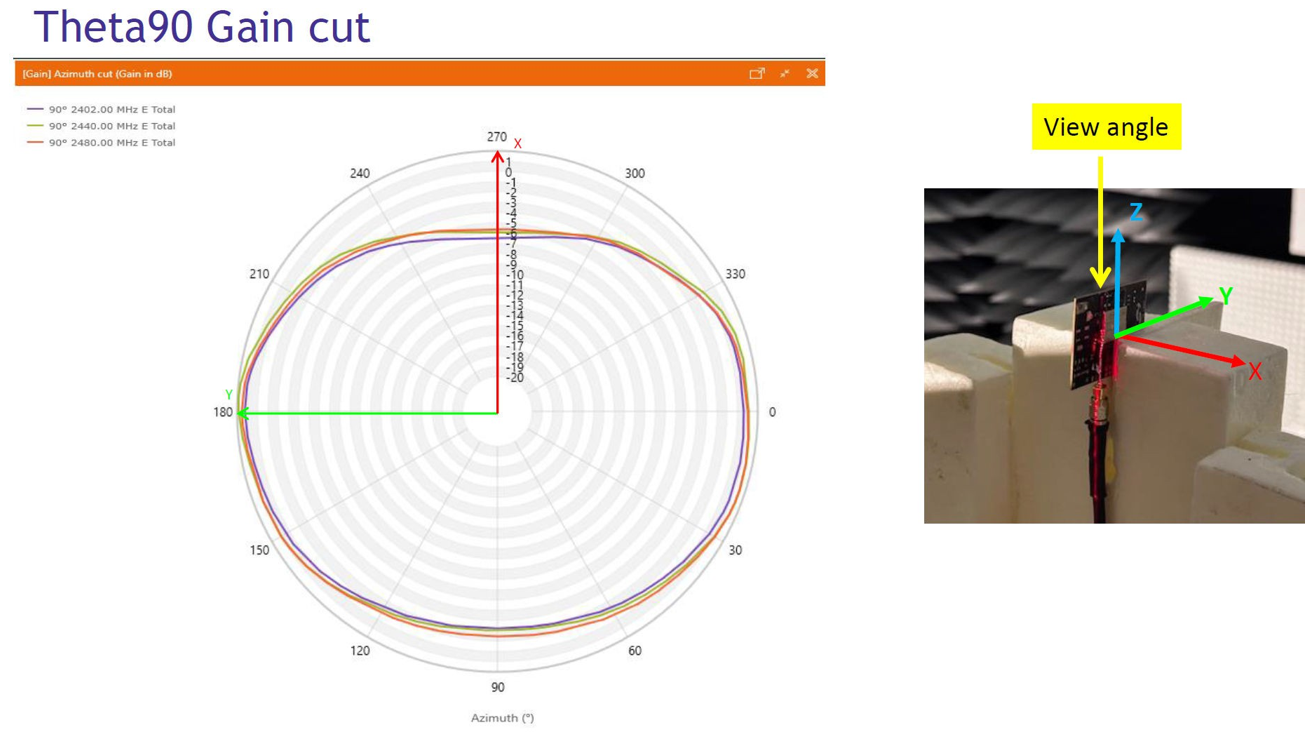
Proximity to Other Materials
Avoid placing plastic or any other dielectric material in close proximity to the antenna. Conformal coating and other thin dielectric layers are acceptable directly on top of the antenna region, but this will also negatively impact antenna efficiency and reduce range.
Any metallic objects in close proximity to the antenna will prevent the antenna from radiating freely. The minimum recommended distance of metallic and/or conductive objects is 10 mm in any direction from the antenna except in the directions of the application PCB ground planes.
Proximity to Human Body
Placing the module in contact with or very close to the human body will negatively impact antenna efficiency and reduce range.
Note: When it comes to modular certifications, following the manufacturer's design guidelines is critical for ensuring that compliance is maintained and modular approvals remain valid, in particular with regards to the carrier (host) PCB size, thickness, relative permittivity, and/or module placement. A modular certification is still valid if no antenna tuning is applied to compensate for reduced performance in terms of range, which may result from sub-optimal carrier PCB size, thickness, relative permittivity, module placement, and/or proximity to other materials such as assembly housing. Conversely, a custom antenna tuning might invalidate a modular certification, unless it is done to compensate for the degradation caused by a printed circuit board deviating from the manufacturer’s best-case reference design in terms of size, thickness, relative permittivity, and/or module placement. In such case, a Permissive Change to a modular approval might become necessary, depending on the resulting performance of the end-product relative to the certified module's test reports, in particular with regards to spurious emission levels, as found during spot-checking. For example, in the FCC case, a Class 1 Permissive Change (C1PC) is considered if the host PCB modifications do not increase emissions. Class 2 Permissive Change (C2PC) is considered if the modifications degrade the emissions but remain below regulatory limits. Whether antenna tuning is applied or not, it is strongly recommended that spot-checking is performed in any case with the end-product having the transmitter(s) operating, to confirm that the host product meets all regulatory requirements under any circumstance. In the end, the emission levels established in the module certification are limits for the end device too and determine whether or not a Permissive Change should be considered. Since this is evaluated on a case-by-case basis, integrators must consult with the company providing certification services for their final product to identify the best approach.
PCB Layout
PCB Layout on Host PCB - 453-00220 Module
Below shows the recommended layout for 453-00220 when using an RF connector for an external antenna. The short RF trace from the RF pad of the module to the pad of the connector must be 50 ohm and exactly the same width as the RF pad of the module, i.e., 700 μm. The below shows two examples on practical implementations of such a trace. The widths S is fixed to 700 um. The height h depends on the PCB stack- up, and the gap width W is adjusted until the impedance of the trace is exactly 50 ohm. Online calculators for coplanar waveguide with ground can be used to calculate the width W for any specific PCB stack-up. The integrator must consider using a unique connector, such as a “reverse polarity SMA” or “reverse thread SMA”, if detachable antenna is offered with the host chassis.
Ground vias underneath the module must be used extensively especially around the rectangular GND pins to enable heat transfer from the bottom of the module to the GND plane of the host board. Routing signal lines elsewhere underneath the module is acceptable.
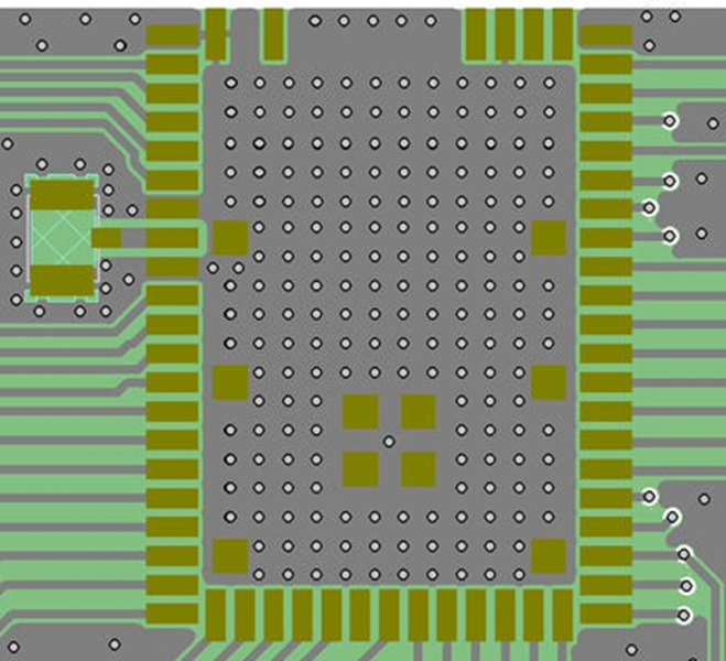
The typical permittivity of PCB laminate is 4.6. If assuming permittivity of 4.6, in the example shown below the dimensions would be:
S = 700 um
h = 420 um W = 332 um
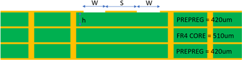
Similarly, if assuming permittivity of 4.6, in the example shown below the dimensions would be:
S = 700 um
h = 730 um W = 132 um
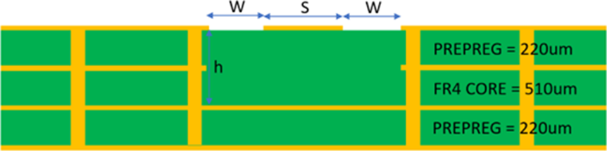
PCB Layout on Host PCB - 453-00222 Integrated Antenna Module
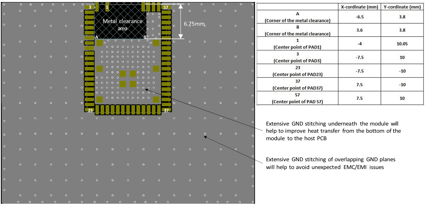
For optimal performance of the 453-00222:
- Place the module aligned to the edge of the application PCB, as illustrated above.
- Leave the antenna clearance area void of any traces, components, or copper on all layers of the application PCB.
- Connect all ground pads directly to a solid ground plane.
- Place the ground vias as close to the ground pads as possible.
- Avoid plastic or any other dielectric material in direct contact with the antenna.
The figure below shows example layout scenarios which will lead to degraded performance and possible EMC issues with the module.
Ground vias underneath the module must be used extensively especially around the rectangular GND pins to enable heat transfer from the bottom of the module to the GND plane of the host board. Routing signal lines elsewhere underneath the module is acceptable.
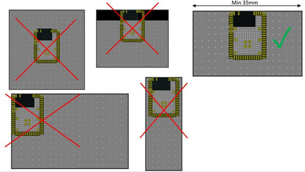
Antennas are by nature affected by the surrounding PCB design and in particular the size and shape of the ground surrounding the antenna. The wide band antenna of 453-00222 is designed to operate in various size/shape application boards and the antenna is not sensitive to dielectric material near the antenna. However, in certain extreme circumstances, such as extremely small board or narrow board, the antenna can be detuned enough to have an impact to the range, EVM characteristics and in-band emissions. In such cases it is possible to fine tune the antenna by using one or two external capacitors or inductors connected between the ANT_TUNE1 and GND and/or ANT_TUNE2 and GND. An example is shown below. Finding the correct value for these components requires empirical testing and measuring the antenna return loss. (See the note below on modular certification.)
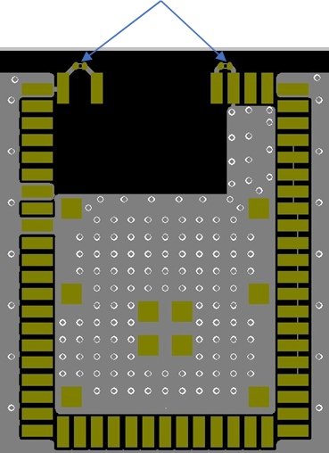
The best antenna performance is achieved when the board width is 50mm and the antenna is placed at the center of the board edge. Having wider or narrower PCB will have up to 25% impact to the range. If the board is narrower than 35mm or wider than 100 mm, it is possible that external fine tuning becomes necessary to maintain the EVM performance.
Application Note for Surface Mount Modules
Soldering Profile / Baking Conditions
It is recommended that final PCB assembly of the SL917 follows the industry standard as identified by the Institute for Printed Circuits (IPC). This product is assembled in compliance with the J-STD-001 requirements and the guidelines of IPC-AJ-820. Surface mounting of this product by the end user is recommended to follow IPC-A-610 to meet or exceed class 2 requirements.
CLASS 1 General Electronic Products
Includes products suitable for applications where the major requirement is function of the completed assembly.
CLASS 2 Dedicated Service Electronic Products
Includes products where continued performance and extended life is required, and for which uninterrupted service is desired but not critical. Typically the end-use environment would not cause failures.
CLASS 3 High Performance/Harsh Environment Electronic Products
Includes products where continued high performance or performance-on-demand is critical, equipment downtime cannot be tolerated, end-use environment may be uncommonly harsh, and the equipment must function when required, such as life support or other critical systems.
Note: General SMT application notes are provided in AN1223: LGA Manufacturing Guidance.
Shipping and Labeling
Packaging
Tape and Reel
The SL917 modules are delivered to the customer in cut tape (100 pcs) or reel (1000 pcs) packaging having the dimensions below. All dimensions are given in mm unless otherwise indicated.
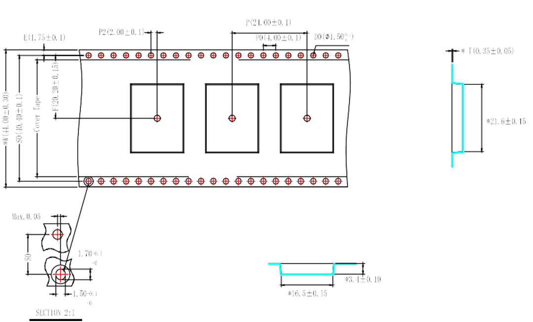

Labeling
Module Marking Information

Environmental and Reliability
Environmental Requirements
Moisture Sensitivity Level
SL917 modules are rated MSL3 (Moisture Sensitivity Level 3). Reels are delivered in packing which conforms to MSL3 requirements.
Regulatory, Qualification & Certifications
Regulatory Approvals
Note: For complete regulatory information, refer to the Veda SL917 Regulatory Information Guide.
The Veda SL917 holds current certifications in the following countries:
| Country/Region | Regulatory ID |
|---|---|
| USA (FCC) | SQG-SL917 |
| Canada (ISED) | 3147A-SL917 |
| UK (UKCA) | *No Regulatory ID required |
| EU | *No Regulatory ID required |
| China (SRRC) | PENDING |
| Japan (MIC) | PENDING |
| Taiwan (NCC) | PENDING |
| Korea (KC) | PENDING |
| Australia (AS) | *No Regulatory ID required |
| New Zealand (NZS) | *No Regulatory ID required |
Certified Antennas
The Veda SL917 SoC modules have been tested and certified for the use with respectively the built-in integral antenna and a reference external antenna attached to the module's RF pin denoted as RF_PORT. The intended antenna impedance is 50 Ω. Because these modules and their associated set of approved antennas has been certified by the FCC and Innovation, Science and Economic Development, Canada (ISED) as Modular Radios, the end user is authorized to integrate this module into an end-product and is solely responsible for the Unintentional Emissions levels produced by the end-product.
To uphold the Modular Radio certifications, the integrator of the module must abide by the PCB layout recommendations outlined in the following paragraphs. Any divergence from these recommendations will invalidate the modular radio certifications and require the integrator to re-certify the module and/or end-product.
Performance characteristics for the built-in antenna are presented in Antenna Characteristics. The details of the qualified external antenna(s) are summarized below. The qualified external antenna(s) is(are) meant to be directly connected to the module's RF pin, with no active/non-linear component(s) along the RF path in between.
| Manufacturer and Model | Type | Peak Gain | Impedance |
|---|---|---|---|
| TE Connectivity Ltd. (previously Linx Technologies Inc.), ANT-2.4-CW-CT-RPS | Connectorized Coaxial Dipole | +2.8 dBi | 50 Ω |
| Ezurio (Laird Connectivity) 001-0022 | FlexPIFA | +2.0 dBi | 50 Ω |
| Ezurio (Laird Connectivity) 001-0023 | FlexNOTCH | +2.0 dBi | 50 Ω |
| Ezurio (Laird Connectivity) EBL2400A1-10MH4L | NanoBlue | +2.0 dBi | 50 Ω |
| Ezurio (Laird Connectivity) EFG2401A3S-10MH4L | i-FlexPIFA Mini | +2.0 dBi | 50 Ω |
| Ezurio (Laird Connectivity) EFG2400A3S-10MH4L | i-FlexPIFA | +3.1 dBi | 50 Ω |
| Ezurio (Laird Connectivity) EFA2400A3S-10MH4L | mFlexPIFA | +2.0 dBi | 50 Ω |
When using the module and the reference design that supports the off module MH4 connector(s), you may use a substitute antenna if it is of the same type and that the gain is less than or equal to the smallest gain for that type for each of the frequencies listed. The OEM is free to choose another vendor’s antenna of like type and equal or lesser gain as an antenna appearing in the table and still maintain compliance. Reference FCC Part 15.204(c)(4) for further information on this topic.
When using instead an external antenna of a different type (such as a chip antenna, a host PCB trace antenna, or a patch) or having non-similar in-band and out-of-band characteristics, but still with a gain less than or equal to the maximum gain listed in the table above, in principle it can be added to the existing modular grant/certificate by mean of a permissive change, for example with FCC and ISED. Typically, some radiated emission testing is demanded, but no modular or end-product re-certification is required. Please consult your certification house and/or a certification body and/or the module manufacturer for a confirmation of the correct procedures and for any authorization to perform permissive changes.
On the other hand, all products designed to be used with an external antenna having more gain than the maximum gain listed in the table above are very likely to require a full new end-product certification. Since the exact permissive change or registration or re-certification procedure is chosen on a case-by-case basis, please consult your certification house and/or a certification body for understanding the correct approach based on your unique design. You might also want or need to get in touch with Ezurio for any authorization letter that your certification body might ask for.
In countries applying the ETSI standards, where manufacturers issue a self-Declaration of Conformity before placing their end-products in the market, like in the EU countries (and in the UK), the radiated emissions are always evaluated with the end-product and the external antenna type is not critical, but antennas with higher gain may violate some of the EIRP regulatory limits.
For Japan, where compliance testing is done conductively, the allowed external antennas are listed in the certificate and/or test report(s). Any other external antenna will have to be formally added to the list of approved antennas by the certificate holder: in this case, please reach out to the module manufacturer to discuss such additions or consider certifying the end-product itself as an alternative.
Federal Communications Commission Interference Statement
This equipment has been tested and found to comply with the limits for a Class B digital device, pursuant to Part 15 of the FCC Rules. These limits are designed to provide reasonable protection against harmful interference in a residential installation. This equipment generates, uses and can radiate radiofrequency energy and, if not installed and used in accordance with the instructions, may cause harmful interference to radio communications. However, there is no guarantee that interference will not occur in a particular installation. If this equipment does cause harmful interference to radio or television reception, which can be determined by turning the equipment off and on, the user is encouraged to try to correct the interference by one of the following measures:
- Reorient or relocate the receiving antenna.
- Increase the separation between the equipment and receiver.
- Connect the equipment into an outlet on a circuit different from that to which the receiver is connected.
- Consult the dealer or an experienced radio/TV technician for help.
FCC Caution: Any changes or modifications not expressly approved by the party responsible for compliance could void the user's authority to operate this equipment.
This device complies with Part 15 of the FCC Rules. Operation is subject to the following two conditions: (1) This device may not cause harmful interference, and (2) this device must accept any interference received, including interference that may cause undesired operation.
Radiation Exposure Statement
This equipment complies with FCC radiation exposure limits set forth for an uncontrolled environment. This equipment should be installed and operated with minimum distances equal or above those being reported in Table 12.2. Minimum Separation Distances for SAR Evaluation Exemption.
This transmitter must not be co-located or operating in conjunction with any other antenna or transmitter.
Integration Instructions for Host Product Manufacturers
Applicable FCC rules to module: FCC Part 15.247
Summary of the specific operational use conditions:
This device is intended only for OEM integrators under the following condition:
The transmitter module may not be co-located with any other transmitter antenna.
If the condition above is met, further transmitter test will not be required. However, the OEM integrator is still responsible for testing their end-product for any additional compliance requirements required with this module installed.
IMPORTANT NOTE: If these conditions cannot be met (for example certain laptop configurations or co-location with another transmitter), then the FCC authorization is no longer considered valid, and the FCC ID cannot be used on the final product. In these circumstances, the OEM integrator will be responsible for re-evaluating the end-product (including the transmitter) and obtaining a separate FCC authorization. The OEM integrator must be aware not to provide information to the end user regarding how to install or remove this RF module in the user’s manual of the end-product which integrates this module.
The end user manual shall include all required regulatory information/warning as shown in this manual.
Limited module procedures
Not applicable
RF exposure considerations
Co-located issue shall be met as mentioned in Summary of the specific operational use conditions.
Product manufacturer shall provide the following text in the end-product manual:
FCC Radiation Exposure Statement
The product complies with the US portable RF exposure limit set forth for an uncontrolled environment and are safe for intended operation as described in this manual. The further RF exposure reduction can be achieved if the product can be kept as far as possible from the user body or set the device to lower output power if such function is available.
A 5.5-centimeter separation distance and co-located issue shall be met as mentioned in Summarize the specific operational use conditions.
Product manufacturer shall provide the following text in the end-product manual:
This equipment complies with FCC radiation exposure limits set forth for an uncontrolled environment. This equipment should be installed and operated with a minimum distance of 5.5 centimeters between the radiator and your body.
Label and Compliance Information
Product manufacturers must provide, with the finished product, a physical or e-label that states the following:
Contains FCC ID: SQG-SL917
Additional Testing, Part 15 Subpart B Disclaimer
The module is only FCC authorized for the specific rule parts listed on the grant, and that the host product manufacturer is responsible for compliance to any other FCC rules that apply to the host not covered by the modular transmitter grant of certification. The final host product still requires Part 15 Subpart B compliance testing with the modular transmitter installed.
Applicable ISED rules to module: RSS-247
This device contains licence-exempt transmitter(s)/receiver(s) that comply with Innovation, Science and Economic Development Canada’s licence-exempt RSS(s). Operation is subject to the following two conditions:
(1) This device may not cause interference
(2) This device must accept any interference, including interference that may cause undesired operation of the device.
L’émetteur/récepteur exempt de licence contenu dans le présent appareil est conforme aux CNR d’Innovation, Sciences et Développement économique Canada applicables aux appareils radio exempts de licence. L’exploitation est autorisée aux deux conditions suivantes :
(1) L’appareil ne doit pas produire de brouillage;
(2) L’appareil doit accepter tout brouillage radioélectrique subi, même si le brouillage est susceptible d’en compromettre le fonctionnement.
This radio transmitter (IC: 3147A-SL917) has been approved by Innovation, Science and Economic Development Canada to operate with the antenna types listed in Table 12.1 above, with the maximum permissible gain indicated. Antenna types not included in this list that have a gain greater than the maximum gain indicated for any type listed are strictly prohibited for use with this device.
Le présent émetteur radio (IC: 3147A-SL917) a été approuvé par Innovation, Sciences et Développement économique Canada pour fonctionner avec les types d'antenne énumérés ci ci-dessus dans le tableau 4 et ayant un gain admissible maximal. Les types d'antenne non inclus dans cette liste, et dont le gain est supérieur au gain maximal indiqué pour tout type figurant sur la liste, sont strictement interdits pour l'exploitation de l'émetteur.
Radiation Exposure Statement:
This equipment complies with Canada radiation exposure limits set forth for an uncontrolled environment. This equipment should be installed and operated with minimum distance 3.5cm between the radiator & your body.
Déclaration d'exposition aux radiations:
Cet équipement est conforme Canada limites d'exposition aux radiations dans un environnement non contrôlé. Cet équipement doit être installé et utilisé à distance minimum de 3.5cm entre le radiateur et votre corps.
This device is intended only for OEM integrators under the following conditions:
- The transmitter module may not be co-located with any other transmitter or antenna.
As long as the condition above is met, further transmitter testing is not required. However, the OEM integrator is still responsible for testing their end-product for any additional compliance requirements required with this module installed.
Cet appareil est conçu uniquement pour les intégrateurs OEM dans les conditions suivantes:
- Le module émetteur peut ne pas être coïmplanté avec un autre émetteur ou antenne.
Tant que les 1 condition ci-dessus sont remplies, des essais supplémentaires sur l'émetteur ne seront pas nécessaires. Toutefois, l'intégrateur OEM est toujours responsable des essais sur son produit final pour toutes exigences de conformité supplémentaires requis pour ce module installé.
IMPORTANT NOTE: If these conditions cannot be met (for example certain laptop configurations or co-location with another transmitter), then the Canada authorization is no longer considered valid, and the IC ID cannot be used on the final product. In these circumstances, the OEM integrator will be responsible for re-evaluating the end product (including the transmitter) and obtaining a separate Canada authorization.
NOTE IMPORTANTE: Dans le cas où ces conditions ne peuvent être satisfaites (par exemple pour certaines configurations d'ordinateur portable ou de certaines co-localisation avec un autre émetteur), l'autorisation du Canada n'est plus considéré comme valide et l'ID IC ne peut pas être utilisé sur le produit final. Dans ces circonstances, l'intégrateur OEM sera chargé de réévaluer le produit final (y compris l'émetteur) et l'obtention d'une autorisation distincte au Canada.
End Product Labelling
The end product must be labelled in a visible area with the following: “Contains IC: 3147A-SL917”.
Plaque signalétique du produit final
Le produit final doit être étiqueté dans un endroit visible avec l'inscription suivante: "Contient des IC: 3147A-SL917.
Manual Information to the End User
The OEM integrator must be aware not to provide information to the end user regarding how to install or remove this RF module in the user’s manual of the end product which integrates this module.
The end user manual shall include all required regulatory information/warning as show in this manual.
Manuel d'information à l'utilisateur final
L'intégrateur OEM doit être conscient de ne pas fournir des informations à l'utilisateur final quant à la façon d'installer ou de supprimer ce module RF dansle manuel de l'utilisateur du produit final qui intègre ce module.
Le manuel de l'utilisateur final doit inclure toutes les informations réglementaires requises et avertissements comme indiqué dans ce manuel.
RF Exposure and Proximity to the Human Body
When using the Veda SL917 modules in an application where the radio-equipped end-product is located close to the human body, the human RF Exposure must be considered. FCC, ISED, and CE/UKCA all have different standards and rules for evaluating the RF Exposure. Each regulator has different requirements when it comes to the exemption from having to perform RF Exposure and SAR (Specific Absorption Rate) measurements, and the minimum separation distances between the module's antenna and the human body varies accordingly. The properties of the Veda SL917 modules allow the minimum separation distances detailed in the table below for the SAR evaluation exemption in the Portable use cases (less than 20 cm from the human body). These modules are approved for the Mobile use case (more than 20 cm) without any need for RF Exposure evaluation.
| Certification | Veda SL917 |
|---|---|
| USA (FCC) | Wi-Fi 802.11b/g/n/ax: 55 mm BLE: 10 mm |
| Canada (ISED) | Wi-Fi 802.11b/g/n/ax: 35 mm BLE: 20 mm |
| EU (CE) / UK (UKCA) | The RF exposure should always be evaluated with the end-product when transmitting with EIRP power levels higher than 20 mW (13 dBm) while at a closer than 20cm distance from the human body. With the Veda SL917 modules, this is the case only with the 802.11b/g/n/ax protocols operating at full power, in particular when the distance is TBD cm and below. In all other cases, modules comply with the requirements of the relevant standard(s) |
Bluetooth SIG Qualification
The Bluetooth Qualification Process promotes global product interoperability and reinforces the strength of the Bluetooth® brand and ecosystem to the benefit of all Bluetooth SIG members. The Bluetooth Qualification Process helps member companies ensure their products that incorporate Bluetooth technology comply with the Bluetooth Patent & Copyright License Agreement and the Bluetooth Trademark License Agreement (collectively, the Bluetooth License Agreement) and Bluetooth Specifications.
The Bluetooth Qualification Process is defined by the Qualification Program Reference Document (QPRD) v3.
To demonstrate that a product complies with the Bluetooth Specification(s), each member must for each of its products:
- Identify the product, the design included in the product, the Bluetooth Specifications that the design implements, and the features of each implemented specification
- Complete the Bluetooth Qualification Process by submitting the required documentation for the product under a user account belonging to your company
The Bluetooth Qualification Process consists of the phases shown below:

To complete the Qualification Process the company developing a Bluetooth End Product shall be a member of the Bluetooth SIG. To start the application please use the following link: Apply for Adopter Membership
Scope
This guide is intended to provide guidance on the Bluetooth Qualification Process for End Products that reference multiple existing designs, that have not been modified, (refer to Section 3.2.2.1 of the Qualification Program Reference Document v3).
For a Product that includes a new Design created by combining two or more unmodified designs that have DNs or QDIDs into one of the permitted combinations in Table 3.1 of the QPRDv3, a Member must also provide the following information:
- DNs or QDIDs for Designs included in the new Design
- The desired Core Configuration of the new Design (if applicable, see Table 3.1 below)
- The active TCRL Package version used for checking the applicable Core Configuration (including transport compatibility) and evaluating test requirements
Any included Design must not implement any Layers using withdrawn specification(s).
When creating a new Design using Option 2a, the Inter-Layer Dependency (ILD) between Layers included in the Design will be checked based on the latest TCRL Package version used among the included Designs.
For the purposes of this document, it is assumed that the member is combining unmodified Core-Controller Configuration and Core-Host Configuration designs, to complete a Core-Complete Configuration.
Qualification Steps When Referencing multiple existing designs, (unmodified) – Option 2a in the QPRDv3
For this qualification option, follow these steps:
- To start a listing, go to: https://qualification.bluetooth.com/
- Select Start the Bluetooth Qualification Process.
Product Details to be entered:
- Project Name (this can be the product name or the Bluetooth Design name).
- Product Description
- Model Number
- Product Publication Date (the product publication date may not be later than 90 days after submission)
- Product Website (optional)
- Internal Visibility (this will define if the product will be visible to other users prior to publication)
- If you have multiple End Products to list then you can select ‘Import Multiple Products’, firstly downloading and completing the template, then by ‘Upload Product List’. This will populate Qualification Workspace with all your products.
Specify the Design:
- Do you include any existing Design(s) in your Product? Answer Yes, I do.
- Enter the multiple DNs or QDIDs used in your, (for Option 2a two or more DNs or QDIDs must be referenced)
- Select ‘I’m finished entering DN’s
- Once the DNs or QDIDs are selected they will appear on the left-hand side, indicating the layers covered by the design (should show Core-Controller and Core Host Layers covered).
- What do you want to do next? Answer, ‘Combine unmodified Designs’.
- The Qualification Workspace Tool will indicate that a new Design will be created and what type of Core-Complete configuration is selected.
- An active TCRL will be selected for the design.
- Perform the Consistency Check, which should result in no inconsistencies
- If there are any inconsistencies these will need to be resolved before proceeding
- Save and go to Test Plan and Documentation
Test Plan and Documentation
- As no modifications have been made to the combined designs the tool should report the following message:
‘No test plan has been generated for your new Design. Test declarations and test reports do not need to be submitted. You can continue to the next step.’ - Save and go to Product Qualification fee
- As no modifications have been made to the combined designs the tool should report the following message:
Product Qualification Fee:
- It’s important to make sure a Prepaid Product Qualification fee is available as it is required at this stage to complete the Qualification Process.
- Prepaid Product Qualification Fee’s will appear in the available list so select one for the listing.
- If one is not available select ‘Pay Product Qualification Fee’, payment can be done immediately via credit card, or you can pay via Invoice. Payment via credit will release the number immediately, if paying via invoice the number will not be released until the invoice is paid.
- Once you have selected the Prepaid Qualification Fee, select ‘Save and go to Submission’
Submission:
- Some automatic checks occur to ensure all submission requirements are complete.
- To complete the listing any errors must be corrected
- Once you have confirmed all design information is correct, tick all of the three check boxes and add your name to the signature page.
- Now select ‘Complete the Submission’.
- You will be asked a final time to confirm you want to proceed with the submission, select ‘Complete the Submission’.
- Qualification Workspace will confirm the submission has been submitted. The Bluetooth SIG will email confirmation once the submission has been accepted, (normally this takes 1 working day).
Download Product and Design Details (SDoC):
- You can now download a copy of the confirmed listing from the design listing page and save a copy in your Compliance Folder
For further information, please refer to the following webpage:
https://www.bluetooth.com/develop-with-bluetooth/qualification-listing/
Example Design Combinations
The following gives an example of a possible design under option 2a:
Ezurio Core Controller + Zephyr Core Host Software Stack (Ezurio Veda SL917-based design)
| Design Name | Listing Type | Owner | Declaration ID | QD ID / DN | Link to listing on the SIG website |
| Veda SL917 | Core Controller | Ezurio | N/A | Q382245 | https://qualification.bluetooth.com/ListingDetails/324124 |
| Simplicity SDK for Zephyr v2025.12.0 and above | Core Host | Silicon Laboratories | N/A | Q379004 | https://qualification.bluetooth.com/ListingDetails/321296 |
An alternative Core Host option is listed below, select only one Core Host for your new design:
| Design Name | Listing Type | Owner | Declaration ID | QD ID / DN | Link to listing on the SIG website |
| SiWx91x Host Subsystem based on Core Specification 5.4 | Core Host | Silicon Laboratories | D066772 | 226680 | https://qualification.bluetooth.com/ListingDetails/93911 |
Qualify More Products
If you develop further products based on the same design in the future, it is possible to add them free of charge. The new product must not modify the existing design i.e add ICS functionality, otherwise a new design listing will be required.
To add more products to your design, select ‘Manage Submitted Products’ in the Getting Started page, Actions, Qualify More Products. The tool will take you through the updating process.
Ordering Information
| Part # | Description |
|---|---|
| 453-00220R | Module, Veda SL917, 8MB Flash, SoC, Trace Pad, Tape and Reel |
| 453-00220C | Module, Veda SL917, 8MB Flash, SoC, Trace Pad, Cut Tape |
| 453-00222R | Module, Veda SL917, 8MB Flash, SoC, Integrated Antenna, Tape and Reel |
| 453-00222C | Module, Veda SL917, 8MB Flash, SoC, Integrated Antenna, Cut Tape |
| 453-00222-K1 | Development Kit, Module, Veda SL917, 8MB Flash, SoC, Integrated Antenna |
Legacy - Revision History
| Version | Date | Notes | Contributors | Approver |
|---|---|---|---|---|
| 0.7 | 19 Feb 2025 | Initial Release | Dave Drogowski Dave Neperud | Andy Ross |
| 0.8 | 2 May 2025 | Added sections 12.1 – 12.4 on qualified Ezurio antennas, FCC, ISED, and RF exposure statements | Dave Neperud |
Preliminary Revision History
Revision 0.7
November, 2024
- Updated Cover page
- Updated Feature List
Added the following sections:
- Removed IR Decoder
- Updated Figure 5.2 Power States on page 27
- Updated Table 5.9 List of Wakeup Sources in Different States on page 30
- Updated 5.6.1 Digital Peripherals and Interfaces
- Updated Table 6.2 Chip Packages - RF and Control Interfaces on page 59
- Updated Table 6.4 Chip Packages - Perpheral Interfaces on page 61
- Updated 6.3 GPIO Pin Multiplexing and reformatted subsection tables.
- Updated 6.4 Valid GPIO Sets for Peripherals
- Updated 6.5.1 Digital Functions
- Updated 6.5.2 Analog Functions
Updated the following Electrical Specifications:
- 7.1 Absolute Maximum Ratings
- 7.2 Recommended Operating Conditions
- 7.3.1 RESET_N Pin
- 7.3.2 Power On Control (POC) and Reset
- 7.3.3 Blackout Monitor
- 7.3.5 Digital I/O Signals
- 7.3.5.1 Open-Drain I2C Pins
- 7.4.2 SDIO 2.0 Secondary
- 7.4.3 HSPI Secondary
- Removed UART
- 7.4.4 GPIO Pins
- 7.4.5 In-Package Flash Memory
- 7.4.6 QSPI
- 7.4.7 PSRAM
- 7.4.8 I2C
- 7.4.9 I2S/PCM Primary and Secondary
- 7.4.10 ULP I2S/PCM Primary and Secondary
- 7.4.11 SSI Primary/Secondary
- 7.4.12 ULP SSI Primary
- Removed SGPIO/MC-PWM/QEI/SCT Timer/SIO Interfaces and USART
- 7.4.13 GSPI Primary
- 7.4.14 Cortex-M4 JTAG
- 7.4.15 Cortex-M4 Trace
- 7.5 Analog Peripherals
- 7.5.4 Analog to Digital Converter
- 7.5.5 Digital to Analog Convertor
- 7.5.6 Op-Amp
- 7.5.7 Temperature Sensor
- Added Note to 8.4.2 Proximity to Human Body
Revision 0.52
October, 2024
- Updated Notes in 1. Feature List
- Updated 2. Ordering Information
- Reformatted all the tables in Section
- Updated Section 7.6 RF Characteristics
- Updated 12.11 Bluetooth Qualification
Revision 0.5
June, 2024
- Updated Features List
- Update Block Diagrams
- Updated System Overview
- Updated Pin Definitions
- Updated Electrical Specifications
- Updated Reference Schematics, BOM and Layout Guidelines
- Updated Certifications
Revision 0.4
April, 2024
NDA release and full update from previous version.
Revision 0.1
August, 2023 Preliminary version