/filters:background_color(white)/2024-10/60-Som-Render-331.png)
Introduction
Introduction
This guide contains tutorials for working with the 60 Series SOM Development board.
Ezurio’s 60 Series SOM brings all of Ezurio’s industry competence and capabilities into one solution. The SOM provides:
- Superior enterprise-class Wi-Fi performance
- Onboard cryptographic engine
- Chain of Trust Architecture with layers of security to mitigate attacks.
- CVE checking and penetration testing
- Reduced time-to-market
- Fully featured development kit for designing with the full suite before integrating with your device.
Additional Resources
Using the AD Converter of the 60 Series SOM DVK
Requirements
- 60-SOM DVK, Power Supply, microUSB cable
- PC with terminal program for accessing the console of the 60-SOM DVK
- Lab power supply to insert voltages and multimeter to verify voltage reading
Setting up
Start by creating a fresh SD card to boot your 60-SOM DVK as described in the 60-SOM Getting Started guide
Download the latest release from the 60-SOM releases page on Github:
When done, insert the freshly written SD card into your 60-SOM DVK and boot:
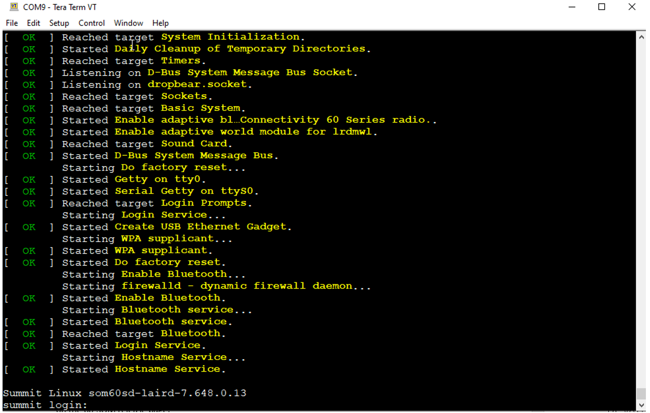
The default username is “root”, and the default password is “summit”.
Summit Linux som60sd-laird-7.648.0.13
summit login: root
Password:
#
Reading the ADC
Query the ADC capabilities of the 60-SOM DVK with the following command:
grep -H "" /sys/bus/iio/devices/*/name | grep adcReply:
# grep -H "" /sys/bus/iio/devices/*/name | grep adc
/sys/bus/iio/devices/iio:device0/name:f8018000.adc
/sys/bus/iio/devices/trigger0/name:f8018000.adc-dev0-external-rising
/sys/bus/iio/devices/trigger1/name:f8018000.adc-dev0-external-falling
/sys/bus/iio/devices/trigger2/name:f8018000.adc-dev0-external-any
/sys/bus/iio/devices/trigger3/name:f8018000.adc-dev0-continuous
As you can see in the reply, there is the ADC “device0”.
Change to the directory for that device and issue the 'ls' command:
cd /sys/bus/iio/devices/iio:device0/
# pwd
/sys/bus/iio/devices/iio:device0
# ls
buffer in_voltage3_raw name
current_timestamp_clock in_voltage4_raw of_node
dev in_voltage5_raw power
in_voltage0_raw in_voltage6_raw scan_elements
in_voltage10_raw in_voltage7_raw subsystem
in_voltage11_raw in_voltage8_raw trigger
in_voltage1_raw in_voltage9_raw uevent
in_voltage2_raw in_voltage_scale
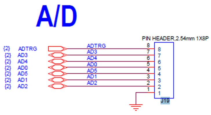
#With referencing the below schematic snippet of the 60-SOM you can see that the following ADC pins are presented at J19 of the DVK:
First read-out
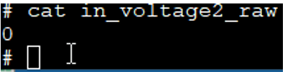
Place a jumper between pin1 and pin2 of J19. This shortens AD2 to GND and the readout should be 0:
Issue the following command:
cat in_voltage2_raw
and you will see the confirmation that the voltage is zero.
 cat-in-voltage2-raw
Other example readout:
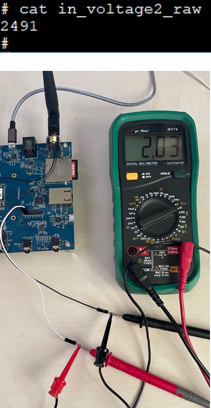
Interpreting the reading
This reading reflects a 12bit ADC. You can verify this in the SAMA5D36 data sheet, available on the SAMAD536 product page at microchip.com.
This is expressed as a decimal in the range of [0 to 4095].
An ADC reading as above of 2491 at a reference voltage of 3.3V (ADVREF) gives us:
3.3V x 2491 / 4095 = 2.01V
Very near to the expected 2V.
Warning: Never exceed the max voltage (3.3V) allowed for the ADC pins!
If in doubt, consult the 60 Series SOM datasheet.
Flash ECC Protection
Introduction
The goal of this document includes the following:
- Define the ECC protection utilized to handle the occurrence of bit flips in the SOM60 NAND flash
Overview
In embedded systems, NOR and NAND Flash memory are complementary solutions with different features and capabilities that serve different purposes.
- NOR memory – Offers faster random read access, allowing for fast boot times and execute-in-place (XiP). This makes it ideal for code storage.
- NAND memory - Offers higher densities, lower cost-per-bit, and fast write performance which is more suitable for data storage.
NAND flash memory's lower cost is enabled by its architecture, which allows memory cells to be designed very close to each other and with fewer contacts. This proximity can cause a failure mechanism commonly known as a bit-flip which results in a bit error. A bit-flip occurs when the floating gate of a NAND cell incorrectly gains or loses electrons. Bit errors due to bit-flips become more likely as the memory wears out due to repeated program/erase cycles. Some NAND flash memory cells may also have inherent defects that make them more likely to experience a bit-flip resulting in a bit error than others on the same die.
NAND flash memory is tested during its manufacturing process to identify cells that are too defective for use, but some weak cells can still pass the screening. The memory manufacturer’s ability to ship NAND with a small percentage of defective cells is major factor in its low cost-per-bit compared with other memory architectures.
All NAND flash components come with NAND's inherent weakness, the potential for bit-flips resulting in bit errors to occur in the field. As a result, NAND flash memory can only be used in systems that also include an error management architecture that can detect and correct bit errors when they occur. The error management is based on an algorithm that uses additional Error Correction and Coding (ECC) bytes that are written along with each block of normal data. The ECC algorithm uses the additional ECC bytes to verify that the data is correct and to correct bit errors when they are detected. The number of bit errors that can be detected and corrected depends on the ECC algorithm used.
Additionally, NAND flash is separated into sectors with enhanced performance. These sectors undergo higher levels of testing and performance checks during manufacture and result in a reduction in the requirements for the capability of the ECC algorithm. This special sector is used for booting the embedded system.
The flash memory (MT29C2G24MAAAAKAMD-5 IT) used on the SOM60 is part of a multi-Layer RAM+flash chip. The Micron datasheet requires that for Sector 0 (boot sector), an algorithm capable of handling a minimum of 1-bit of error per 528 bytes be used to ensure error free performance during the life of the memory. The datasheet requires that the remaining flash memory uses an algorithm of capable of handling a minimum of 4-bits of error per 528 bytes.
ECC algorithm utilized on the SOM60
The SOM60 uses a SAMA5D36 processor from Microchip to read / write data to / from the flash memory chip on the SOM60.
The SAMA5D36 memory controller hardware used in processor embeds a hardware NAND memory controller. This hardware includes a NAND Flash Error Correction Controller. The Error Correction controller corrects the bits as the NAND flash memory is read. The Error Correction Code controller supports 2-bit, 4-bit, 8-bit and 16-bit errors per 528bytes. The Error Correction controller is configured at boot, prior to any NAND flash memory reads, to use the algorithm providing 8-bits of error protection per 528 bytes. This is double the level of error correction recommended by Micron for the NAND Flash memory.