/filters:background_color(white)/2024-10/BL654-Series.png)
Introduction
Overview
This document describes key hardware aspects of the BL654 Series modules. This document is intended to assist device manufacturers and related parties with the integration of this radio into their host devices. Data in this document is drawn from several sources. For full documentation on the BL654 series, visit the BL654 product page.
General Description
Every BL654 Series module is designed to simplify OEMs enablement of Bluetooth Low Energy (BLE) v5.3 and Thread (802.15.4) to small, portable, power-conscious devices. The BL654 provides engineers with considerable design flexibility in both hardware and software programming capabilities. Based on the world-leading Nordic Semiconductor nRF52840 chipset, the BL654 modules provide ultra-low power consumption with outstanding wireless range via +8 dBm of transmit power and the Long Range (CODED PHY) Bluetooth 5 feature. The BL654 is programmable via Ezurio’s smartBASIC language or Nordic’s software development kit (SDK).
smartBASIC is an event-driven programming language that is highly optimized for memory-constrained systems such as embedded modules. It was designed to make BLE development quicker and simpler, vastly cutting down time to market.
The Nordic SDK, on the other hand, offers developers source code (in C) and precompiled libraries containing BLE and ANT+ device profiles, wireless communication, as well as application examples.
Note: BL654 hardware provides all functionality of the nRF52840 chipset used in the module design. This is a hardware datasheet only – it does not cover the software aspects of the BL654.
For customers using smartBASIC, refer to the smartBASIC extensions guide (available from the BL654 product page of the Ezurio website. For customers using the Nordic SDK, refer to www.nordicsemi.com.
Note: Nordic SDK is not supported on the BL654 USB dongle, part #451-00003.
Application Areas
- Medical devices
- IoT Sensors
- Appcessories
- Fitness sensors
- Location awareness
- Home automation
Features & Benefits
The BL654 device features and benefits are described below.
- Bluetooth v5.3 – Single mode
- NFC
- 802.15.4 (Thread) radio support
- External or internal antennas
Multiple programming options
- smartBASIC AT command set shim or
- Nordic SDK in C
- Compact footprint
- Programmable Tx power +8 dBm to -20 dBm, -40 dBm
- Rx sensitivity – -95 dBm (1 Mbps), - 103 dBm (125 kbps)
- Ultra-low power consumption
- Tx – 4.8 mA peak (at 0 dBm, DCDC on)
(See Note 1 in the Power Consumption section) - Rx: 4.6 mA peak (DCDC on)
(See Note 1 in the Power Consumption section) - Standby Doze – 3.1 uA typical
- Deep Sleep – 0.4 uA – (See Note 4 in the Power Consumption section)
- UART, GPIO, ADC, PWM, FREQ output, timers, I2C, SPI, I2S, PDM, and USB interfaces
- Fast time-to-market
- FCC, EU, ISED, RCM and Japan certified
- Full Bluetooth Declaration ID
- Other regulatory certifications on request
- No external components required
- Industrial temperature range (-40° C to +85° C)
Specification Summary
Processor / SoC
| Chipset | Nordic nRF52840 |
Bluetooth
| Standards | BT 5.3 – Single mode | ||||||||
| Bluetooth Features |
| ||||||||
| Services Supported |
| ||||||||
| Frequency Range | 2.402 - 2.480 GHz | ||||||||
| Max Transmit Power |
| ||||||||
| Min Transmit Power |
| ||||||||
| Receive Sensitivity |
| ||||||||
| Supported Data Rates | 1 Mbps BLE (over-the-air) 2 Mbps BLE (over-the-air) 125 kbps BLE (over-the-air) 500 kbps BLE (over-the-air) | ||||||||
| Link Budget |
| ||||||||
| Bluetooth LE Modulation | Coded PHY 2M PHY | ||||||||
| Bluetooth Media | Frequency Hopping Spread Spectrum (FHSS) |
NFC
| Standards | NHFC-A Listen Mode Compliant NFC Type 2 and Type 4 emulation |
| Frequency Range | 13.56 MHz |
| Supported Data Rates | 106 Kbps |
| Modes of Operation |
|
| Use Cases |
|
| System Wake-On-Field Function | Proximity Detection |
Radio Performance
| Antenna Options | Internal
External
See the External Antenna Integration with the 451-00002 sections for FCC, ISED, MIC, RCM and EU. |
| Peripheral Interface | 48x Multifunction I/O lines |
|---|---|
| UART | 2 UARTs Tx, Rx, CTS, RTS DCD, RI, DTR, DSR (See Note 2 and Note 1 in the Module Specification Notes) Default 115200, n, 8, 1 From 1,200 bps to 1 Mbps |
| USB | USB 2.0 FS (Full Speed, 12Mbps). CDC driver / Virtual UART (baud rate TBD) Other USB drivers available via Nordic SDK |
| GPIO | Up to 48, with configurable: I/O direction, O/P drive strength (standard 0.5 mA or high 3mA/5 mA), Pull-up /pull-down Input buffer disconnect |
| ADC | Eight 8/10/12-bit channels 0.6 V internal reference Configurable 4, 2, 1, 1/2, 1/3, 1/4, 1/5 1/6(default) pre-scaling Configurable acquisition time 3uS, 5uS, 10uS (default), 15uS, 20uS, 40uS. One-shot mode |
| PWM | PWM outputs on 16 GPIO output pins.
|
| FREQ | FREQ outputs on 16 GPIO output pins.
|
| I2C | Two I2C interface (up to 400 kbps) – See Note 3 in the Module Specification Notes |
| SPI | Four SPI Master Slave interface (up to 4 Mbps) |
| QSPI | One 32-MHz QSPI interface. Gives XIP (Execution in Place) capability. External serial flash IC must be fitted as per Nordic specifications. |
| TEMP | One temperature sensor. Temperature range equal to the operating temperature range. Resolution 0.25 degrees. |
| RSSI | One RF received signal strength indicator ±2 dB accuracy (valid over -90 to -20 dBm) One dB resolution |
| I2S | One inter-IC sound interface |
| PDM | One pulse density modulation interface |
| Ext. 32.768 KHz Crystal | For customer use, connect +/-20ppm accuracy crystal for more accurate protocol timing. |
Power
| Input Voltage | Supply (VDD or VDD_HV) options:
| ||||
| Active Modes Peak Current (for maximum Tx power +8 dBm) – Radio only | 14.8 mA peak Tx (with DCDC) | ||||
| Active Modes Peak Current (for Tx power -40 dBm) – Radio only | 4.6 mA peak Tx (with DCDC) | ||||
| Active Modes Average Current | Depends on many factors, see | ||||
| Ultra-low Power Modes |
| ||||
| I/O Signal Voltage |
Mechanical
| Dimensions | 15.0 mm x 10 mm x 2.2 mm Pad Pitch – 0.8 mm Pad Type – Two rows of pads |
| Weight | <1 gram |
Software
| Operating Modes | smartBASIC
Nordic SDK
Note: Nordic SDK is not supported on the BL654 USB dongle, part #451-00003. |
| Firmware Update | smartBASIC:
Nordic SDK:
Note: Nordic SDK is not supported on the BL654 USB dongle, part #451-00003. |
Environmental
| Operating Temperature | -40 ˚C to +85 ˚C |
| Storage Temperature | -40 ˚C to +85 ˚C |
| Lead Free | Lead-free and RoHS COmpliant |
Certifications
| Regulatory Compliance | FCC/ISED/EU/MIC/RCM - All BL654 Series |
| Bluetooth SIG | Full Bluetooth SIG Declaration ID |
Development
| Development Kit | Development kit per module SKU (455-00001 and 455-00002) and free software tools |
Warranty
| Warranty Terms | One Year Warranty |
Module Specification Notes:
| Note 1 | When used in IEEE 802.15.4 mode, 802.15.4 channel 26 must be limited to -8 dBm maximum transmit power to limit out of band emissions. All other 802.15.4 channels (11-25) may be used up to the maximum +8 dBm output power. |
| Note 2 | DSR, DTR, RI, and DCD can be implemented in the smartBASIC application or through the Nordic SDK. Note: Nordic SDK is not supported on the BL654 USB dongle, part #451-00003. |
| Note 3 | With I2C interface selected, pull-up resistors on I2C SDA and I2C SCL must be connected externally as per I2C standard. |
| Note 4 | Use of the internal DCDC convertor or LDO is decided by the underlying BLE stack. |
| Note 5 | Nordic Errata 197 and 202 related to the use of VDD_HV DCDC convertor, for details refer to http://infocenter.nordicsemi.com/pdf/nRF52840_Rev_1_Errata_v1.1.pdf. Nordic Errata 202 means no external current draw (from VDD pin) is allowed during power up and VDD_HV rise time (to 3V) is below one mS. |
Functional Descriptions
Programming & Firmware
BL654 Default Firmware
The BL654 module comes loaded with smartBASIC firmware but does not come loaded with any smartBASIC application script (as that is dependent on customer-end application or use). Ezurio provides many sample smartBASIC application scripts via a sample application folder on GitHub – https://github.com/EzurioCP/BL654-Applications
Therefore, it boots into AT command mode by default.
BL654 Special Function Pins in smartBASIC
Refer to the smartBASIC extension manual for details of functionality connected to this:
- nAutoRUN pin (SIO_35), see Table 6 for default
- VSP pin (SIO_02), see Table 7 for default
- SIO_38 – Reserved for future use. Do not connect. See Table 8
nAutoRUN pin
| Signal Name | Pin # | I/O | Comments |
|---|---|---|---|
| nAutoRUN /(SIO_35) | 5 | I | Input with active low logic. Internal pull down (default). Operating mode selected by nAutoRun pin status:
|
In the development board nAutoRUN pin is connected so that the state is driven by the host’s DTR output line.
VSP mode
| Signal Name | Pin # | I/O | Comments |
|---|---|---|---|
| SIO_02 | 50 | I | Internal pull down (default). VSP mode selected by externally pulling-up SIO_02 pin: High (VCC), then OTA smart BASIC application download is possible. |
SIO_38
| Signal Name | Pin # | I/O | Comments |
|---|---|---|---|
| SIO_38 | 63 | I | Internal pull up (default). Reserved for future use. Do not connect if using smartBASIC FW. |
Interfaces
UART
Note: The BL654 has two UARTs.
The Universal Asynchronous Receiver/Transmitter (UART) offers fast, full-duplex, asynchronous serial communication with built-in flow control support (UART_CTS, UART_RTS) in HW up to one Mbps baud. Parity checking and generation for the ninth data bit are supported.
UART_TX, UART_RX, UART_RTS, and UART_CTS form a conventional asynchronous serial data port with handshaking. The interface is designed to operate correctly when connected to other UART devices such as the 16550A. The signaling levels are nominal 0 V and 3.3 V (tracks VDD) and are inverted with respect to the signaling on an RS232 cable.
Two-way hardware flow control is implemented by UART_RTS and UART_CTS. UART_RTS is an output and UART_CTS is an input. Both are active low.
These signals operate according to normal industry convention. UART_RX, UART_TX, UART_CTS, UART_RTS are all 3.3 V level logic (tracks VDD). For example, when RX and TX are idle they sit at 3.3 V. Conversely for handshaking pins CTS, RTS at 0 V is treated as an assertion.
The module communicates with the customer application using the following signals:
- Port/TxD of the application sends data to the module’s UART_RX signal line
- Port/RxD of the application receives data from the module’s UART_TX signal line
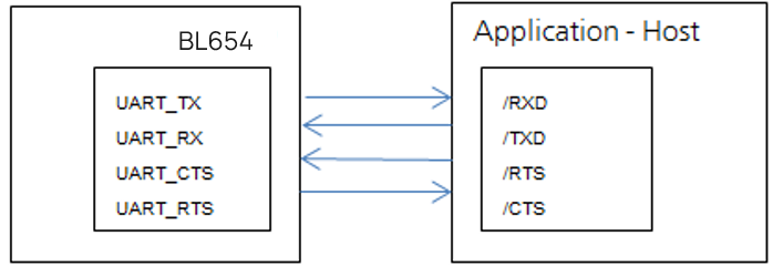
Note: The BL654 serial module output is at 3.3V CMOS logic levels (tracks VDD). Level conversion must be added to interface with an RS-232 level compliant interface.
Some serial implementations link CTS and RTS to remove the need for handshaking. We do not recommend linking CTS and RTS other than for testing and prototyping. If these pins are linked and the host sends data at the point that the BL654 deasserts its RTS signal, there is significant risk that internal receive buffers will overflow, which could lead to an internal processor crash. This will drop the connection and may require a power cycle to reset the module. We recommend that the correct CTS/RTS handshaking protocol be adhered to for proper operation.
UART interface
| Signal Name | Pin # | I/O | Comments |
|---|---|---|---|
| SIO_06 / UART_Tx | 35 | O | SIO_06 (alternative function UART_Tx) is an output, set high (in firmware). |
| SIO_08 / UART_Rx | 29 | I | SIO_08 (alternative function UART_Rx) is an input, set with internal pull-up (in firmware). |
| SIO_05 / UART_RTS | 39 | O | SIO_05 (alternative function UART_RTS) is an output, set low (in firmware). |
| SIO_07 / UART_CTS | 37 | I | SIO_07 (alternative function UART_CTS) is an input, set with internal pull-down (in firmware). |
The UART interface is also used to load customer developed smartBASIC application script.
USB
BL654 has USB2.0 FS (Full Speed, 12Mbps) hardware capability. There is a CDC driver/Virtual UART as well as other USB drivers available via Nordic SDK – such as: usb_audio, usb_hid, usb_generic, usb_msc (mass storage device).
Note: Nordic SDK is not supported on the BL654 USB dongle, part #451-00003.
USB interface
| Signal Name | Pin # | I/O | Comments |
|---|---|---|---|
| D- | 17 | I/O | |
| D+ | 15 | I/O | |
| VBUS | 24 | When using the BL654 VBUS pin (which is mandatory when USB interface is used), Customer MUST connect externally a 4.7uF capacitor to ground. Note: You MUST power the rest of BL654 module circuitry through the VDD pin (OPTION1) or VDD_HV pin (OPTION2). |
SPI Bus
The SPI interface is an alternate function on SIO pins.
The module is a master device that uses terminals SPI_MOSI, SPI_MISO, and SPI_CLK. SPI_CS is implemented using any spare SIO digital output pins to allow for multi-dropping.
The SPI interface enables full duplex synchronous communication between devices. It supports a 3-wire (SPI_MOSI, SPI_MISO, SPI_SCK,) bidirectional bus with fast data transfers to and from multiple slaves. Individual chip select signals are necessary for each of the slave devices attached to a bus, but control of these is left to the application through use of SIO signals. I/O data is double buffered.
The SPI peripheral supports SPI mode 0, 1, 2, and 3.
SPI interfaces
| Signal Name | Pin # | I/O | Comments |
|---|---|---|---|
| SIO_40/SPI_MOSI | 32 | O | This interface is an alternate function configurable by smartBASIC. Default in the FW pin 56 and 53 are SIO inputs. SPIOPEN() in smartBASIC selects SPI function and changes pin 56 and 53 to outputs (when in SPI master mode). |
| SIO_04/AIN2/SPI_MISO | 34 | I | |
| SIO_41/SPI_CLK | 30 | O | |
| Any_SIO/SPI_CS | 54 | I | SPI_CS is implemented using any spare SIO digital output pins to allow for multi-dropping. On Ezurio devboard SIO_44 (pin54) used as SPI_CS. |
I2C
The I2C interface is an alternate function on SIO pins.
The two-wire interface can interface a bi-directional wired-OR bus with two lines (SCL, SDA) and has master /slave topology. The interface is capable of clock stretching. Data rates of 100 kbps and 400 kbps are supported.
An I2C interface allows multiple masters and slaves to communicate over a shared wired-OR type bus consisting of two lines which normally sit at VDD. The SCL is the clock line which is always sourced by the master and SDA is a bi-directional data line which can be driven by any device on the bus.
IMPORTANT: It is essential to remember that pull-up resistors on both SCL and SDA lines are not provided in the module and MUST be provided external to the module.
I2C interface
| Signal Name | Pin # | I/O | Comments |
|---|---|---|---|
| SIO_26/I2C_SDA | 36 | I/O | This interface is an alternate function on each pin, configurable by smartBASIC. I2COPEN() function in smartBASIC selects I2C function. |
NFC
NFC support:
Based on the NFC forum specification
- 13.56 MHz
- Date rate 106 kbps
- NFC Type2 and Type4 tag emulation
Modes of operation:
- Disable
- Sense
- Activated
Use Cases
- Touch-to Pair with NFC
- Launch a smartphone app (on Android)
- NFC enabled Out-of-Band Pairing
System Wake-On-Field function
- Proximity Detection
NFC interface
| Signal Name | Pin # | I/O | Comments |
|---|---|---|---|
| NFC1/SIO_09 | 59 | I/O | The NFC pins are by default NFC pins and an alternate function on each pin is GPIO. Refer to the smartBASIC. User manual. |
| NFC2/SIO_10 | 57 | I/O |
NFC Antenna Coil Tuning Capacitors
From Nordic’s nRF52840 Objective Product Specification v1.0: http://infocenter.nordicsemi.com/pdf/nRF52840_PS_v1.0.pdf
The NFC antenna coil must be the connected differential between the NFC1 and NFC2 pins of the BL654. Two external capacitors should be used to tune the resonance of the antenna circuit to 13.56 MHz.
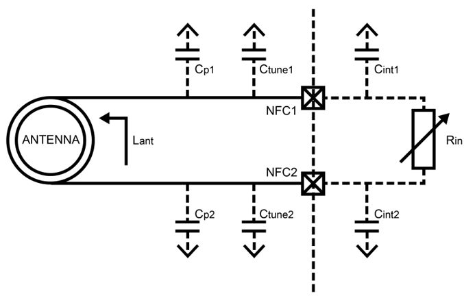
The required external tuning capacitor value is given by the following equations:
An antenna inductance of Lant = 0.72 uH provides tuning capacitors in the range of 300 pF on each pin. The total capacitance on NFC1 and NFC2 must be matched. Cint and Cp are small usually (Cint is 4pF), so can omit from calculation.
Battery Protection Note: If the NFC coil antenna is exposed to a strong NFC field, the supply current may flow in the opposite direction due to parasitic diodes and ESD structures.
If the used battery does not tolerate a return current, a series diode must be placed between the battery and the BL654 to protect the battery.
GPIO
The 19 SIO pins are configurable by smartBASIC application script or Nordic SDK. They can be accessed individually. Each has the following user configured features:
- Input/output direction
- Output drive strength (standard drive 0.5 mA or high drive 5mA)
- Internal pull-up and pull-down resistors (13 K typical) or no pull-up/down or input buffer disconnect
- Wake-up from high or low-level triggers on all pins including NFC pins
ADC
The ADC is an alternate function on SIO pins, configurable by smart BASIC or Nordic SDK.
The BL654 provides access to 8-channel 8/10/12-bit successive approximation ADC in one-shot mode. This enables sampling up to 8 external signals through a front-end MUX. The ADC has configurable input and reference pre-scaling and sample resolution (8, 10, and 12 bit).
Analog Interface (ADC)
| Signal Name | Pin # | I/O | Comments |
|---|---|---|---|
| SIO_05/UART_RTS/AIN3 – Analog Input | 39 | I | This interface is an alternate function on each pin, configurable by smartBASIC. AIN configuration selected using GpioSetFunc() function. Configurable 8, 10, 12-bit resolution. Configurable voltage scaling 4, 2, 1/1, 1/3, 1/3, 1/4, 1/5, 1/6(default). Configurable acquisition time 3uS, 5uS, 10uS(default), 15uS, 20uS, 40uS. Full scale input range (VDD) |
| SIO_04/AIN2/SPI_MISO – Analog Input | 34 | I | |
| SIO_03/AIN1 – Analog Input | 49 | I | |
| SIO_02/AIN0 – Analog Input | 50 | I | |
| SIO_31/AIN7 – Analog Input | 44 | I | |
| SIO_30/AIN6 – Analog Input | 45 | I | |
| SIO_29/AIN5 – Analog Input | 48 | I | |
| SIO_28/AIN4 – Analog Input | 46 | I |
PWM
PWM Signal Output on up to 16 SIO Pins
The PWM output is an alternate function on ALL (GPIO) SIO pins, configurable by smartBASIC or the Nordic SDK.
The PWM output signal has a frequency and duty cycle property. Frequency is adjustable (up to 1 MHz) and the duty cycle can be set over a range from 0% to 100%.
PWM output signal has a frequency and duty cycle property. PWM output is generated using dedicated hardware in the chipset. There is a trade-off between PWM output frequency and resolution.
For example:
- PWM output frequency of 500 kHz (2 uS) results in resolution of 1:2.
- PWM output frequency of 100 kHz (10 uS) results in resolution of 1:10.
- PWM output frequency of 10 kHz (100 uS) results in resolution of 1:100.
- PWM output frequency of 1 kHz (1000 uS) results in resolution of 1:1000.
FREQ
FREQ Signal Output on up to 16 SIO Pins
The FREQ output is an alternate function on 16 (GPIO) SIO pins, configurable by smartBASIC or Nordic SDK.
Note: The frequency driving each of the 16 SIO pins is the same but the duty cycle can be independently set for each pin.
FREQ output signal frequency can be set over a range of 0Hz to 4 MHz (with 50% mark-space ratio).
nReset Pin
nRESET pin
| Signal Name | Pin # | I/O | Comments |
|---|---|---|---|
| nRESET | 19 | I | BL654 HW reset (active low). Pull the nRESET pin low for minimum 100mS for the BL654 to reset. |
Two-Wire Interface JTAG
The BL654 Firmware hex file consists of four elements:
- smartBASIC runtime engine
- Nordic Softdevice
- Master Bootloader
Ezurio BL654 smartBASIC firmware (FW) image part numbers are referenced as w.x.y.z (ex. v29.x.y.z). The BL654 smartBASIC runtime engine and Softdevice combined image can be upgraded by the customer over the UART interface.
You also have the option to use the two-wire (JTAG) interface, during production, to clone the file system of a Golden preconfigured BL654 to others using the Flash Cloning process. This is described in the following application note Flash Cloning for the BL654. In this case the file system is also part of the .hex file.
Two-wire interface JTAG
| Signal Name | Pin # | I/O | Comments |
|---|---|---|---|
| SWDIO | 1 | I/O | Internal pull-up resistor |
| SWDCLK | 3 | I | Internal pull-down resistor |
The Ezurio development board incorporates an on-board JTAG J-link programmer for this purpose. There is also the following JTAG connector which allows on-board JTAG J-link programmer signals to be routed off the development board. The only requirement is that you should use the following JTAG connector on the host PCB.
The JTAG connector MPN is as follows:
JTAG connector MPN
| Reference | Part | Description and MPN (Manufacturer Part Number) |
|---|---|---|
| JP1 | FTSH-105 | Header, 1.27mm, SMD, 10-way, FTSH-105-01-L-DV Samtech |
Note: Reference on the BL654 development board schematic (Figure 7) shows the DVK development schematic wiring only for the JTAG connector and the BL654 module JTAG pins.
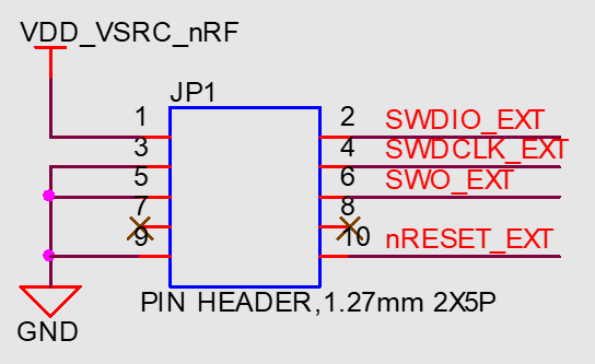
Note: The BL654 development board allows Ezurio on-board JTAG J-link programmer signals to be routed off the development board by from connector JP1
JTAG is require because Nordic SDK applications can only be loaded using the JTAG (smartBASIC firmware can be loaded using JTAG as well as over the UART). We recommend that you use JTAG (2-wire SWD interface) to handle future BL654 module firmware upgrades. You must wire out the JTAG (2-wire SWD interface) on your host design (see Figure 7, where the following four lines should be wired out – SWDIO, SWDCLK, GND and VCC). smartBASIC firmware upgrades can still be performed over the BL654 UART interface, but this is slower than using the BL654 JTAG (2-wire SWD interface) – (60 seconds using UART vs. 10 seconds when using JTAG).
SWO (SIO_32) is a Trace output (called SWO, Serial Wire Output) and is not necessary for programming BL654 over the SWD interface.
nRESET_BLE is not necessary for programming BL654 over the SWD interface.
Note: Nordic SDK is not supported on the BL654 USB dongle, part #451-00003.
BL654 Wakeup
Waking Up BL654 from Host
Wake the BL654 from the host using wake-up pins (any SIO pin). You may configure the BL654’s wakeup pins via smartBASIC to do any of the following:
- Wake up when signal is low
- Wake up when signal is high
- Wake up when signal changes
Refer to the smartBASIC user guide for details. You can access this guide from the Ezurio BL654 product page.
For BL654 wake-up using the Nordic SDK, refer to Nordic infocenter.nordicsemi.com.
Temperature Sensor
The on-silicon temperature sensor has a temperature range greater than or equal to the operating temperature of the device. Resolution is 0.25°C degrees. The on-silicon temperature sensor accuracy is ±5°C.
To read temperature from on-silicon temperature sensor (in tenth of centigrade, so 23.4°C is output as 234) using smartBASIC:
In command mode, use ATI2024
or
From running a smartBASIC application script, use SYSINFO(2024)
Optional External 32.768 kHz crystal
This is not required for normal BL654 module operation.
The BL654 uses the on-chip 32.76 kHz RC oscillator (LFCLK) by default (which has an accuracy of ±500 ppm) which requires regulator calibration (every eight seconds) to within ±500 ppm.
You can connect an optional external high accuracy (±20 ppm) 32.768 kHz crystal (and associated load capacitors) to the BL654SIO_01/XL2 (pin 41) and SIO_00/XL1 (pin 42) to provide improved protocol timing and to help with radio power consumption in the system standby doze/deep sleep modes by reducing the time that the RX window needs to be open. Table 25 compares the current consumption difference between RC and crystal oscillator.
Comparing current consumption difference between BL654 on-chip RC 32.76 kHz oscillator and optional external crystal (32.768kHz) based oscillator
| Reference | BL654 On-chip 32.768 kHz RC Oscillator (±500 ppm) LFRC | Optional External Higher Accuracy (±20 ppm) 32.768 kHz Crystal-based Oscillator LFXO |
|---|---|---|
| Current Consumption of 32.768 kHz Block | 0.7 uA | 0.23 uA |
| Standby Doze Current (SYSTEM ON IDLE +full RAM retention +RTC run current + LFRC or LFXO) | 3.1 uA | 2.6 uA |
| Calibration | Calibration required regularly (default eight seconds interval). Calibration takes 33 ms; with DCDC used, the total charge of a calibration event is 16 uC. The average current consumed by the calibration depends on the calibration interval and can be calculated using the following formula: CAL_charge/CAL_interval – The lowest calibration interval (0.25 seconds) provides an average current of (DCDC enabled): 16uC/0.25s = 64uA To get the 500-ppm accuracy, the BLE stack specification states that a calibration interval of eight seconds is enough. This gives an average current of: 16uC/8s = 2 uA Added to the LFRC run current and Standby Doze (IDLE) base current shown above results in a total average current of: LFRC + CAL = 3.1 + 2 = 5.1 uA | Not applicable |
| Total | 5.1 uA | 2.6 uA |
| Summary | · Low current consumption · Accuracy 500 ppm |
|
Optional external 32.768 kHz crystal specification
| Optional external 32.768kHz crystal | Min | Typ | Max |
|---|---|---|---|
| Crystal Frequency | - | 32.768 kHz | - |
| Frequency tolerance requirement of BLE stack | - | - | ±500 ppm |
| Load Capacitance | - | - | 12.5 pF |
| Shunt Capacitance | - | - | 2 pF |
| Equivalent series resistance | - | - | 100 kOhm |
| Drive level | - | - | 1 uW |
| Input capacitance on XL1 and XL2 pads | - | 4 pF | - |
| Run current for 32.768 kHz crystal-based oscillator | - | 0.23 uA | - |
| Start-up time for 32.768 kHz crystal-based oscillator | - | 0.25 seconds | - |
| Peak to peak amplitude for external low swing clock input signal must not be outside supply rails | 200 mV | - | 1000 mV |
Be sure to tune the load capacitors on the board design to optimize frequency accuracy (at room temperature) so it matches that of the same crystal standalone, Drive Level (so crystal operated within safe limits) and oscillation margin (Rneg is at least 3 to 5 times ESR) over the operating temperature range.
Security and Privacy
Random Number Generator
Exposed via an API in smartBASIC (see smartBASIC documentation available from the BL654 product page). The rand() function from a running smartBASIC application returns a value.
For Nordic related functionality, visit Nordic infocenter.nordicsemi.com
AES Encryption/Decryption
Exposed via an API in smartBASIC (see smartBASIC documentation available from the BL654 product page). Function called aesencrypt and aesdecrypt.
For Nordic related functionality, visit Nordic infocenter.nordicsemi.com
ARM Cryptocell
ARM Cryptocell incorporates a true random generator (TRNG) and support for a wide range of asymmetric, symmetric and hashing cryptographic services for secure applications. For more information, please check the Nordic SDK.
Readback Protection
The BL654 supports readback protection capability that disallows the reading of the memory on the nrf52840 using a JTAG interface. Available via smartBASIC or the Nordic SDK.
Eliptic Curve Cryptography
The BL654 offers a range of functions for generating public/private keypair, calculating a shared secret, as well as generating an authenticated hash. Available via smartBASIC or the Nordic SDK.
RF
- 2402–2480 MHz Bluetooth Low Energy radio BT 5.3 – 1 Mbps, 2 Mbps, and Long-range (125 kbps and 500 kbps) over-the-air data rate.
- Tx output power of +8 dBm programmable down to 7 dBm, 6 dBm, 5 dBm, 4 dBm, 2 dBm, 0 dBm and further down to -20 dBm in steps of 4 dB and final TX power level of -40 dBm.
- Receiver (with integrated channel filters) to achieve maximum sensitivity -95 dBm @ 1 Mbps BLE, -92 dBm @2 Mbps, -103 dBm @ 125 kbps long-range and -99 dBm @500kbps long-range).
RF conducted interface available in the following two ways:
- 451-00001: RF connected to on-board PCB trace antenna
- 451-00002: RF connected to on-board IPEX MH4 RF connector
Antenna options:
- Integrated PCB trace antenna on the 451-00001
- External dipole antenna connected with to IPEX MH4 RF connector on the 451-00002
- Received Signal Strength Indicator (RSSI)
- RSSI accuracy (valid range -90 to -20dBm) is ±2dB typical
- RSSI resolution 1dB typical
Power
Power Management
Power management features:
- System Standby Doze and Deep Sleep modes
- Open/Close peripherals (UART, SPI, QSPI, I2C, SIO’s, ADC, NFC). Peripherals consume current when open; each peripheral can be individually closed to save power consumption
- Use of the internal DCDC convertor or LDO is decided by the underlying BLE stack
- smartBASIC command allows the supply voltage to be read (through the internal ADC)
- Pin wake-up system from deep sleep (including from NFC pins)
Power supply features:
Supervisor hardware to manage power during reset, brownout, or power fail.
- 1.7V to 3.6V supply range for normal power supply (VDD pin) using internal DCDC convertor or LDO decided by the underlying BLE stack.
- 2.5V to 5.5 supply range for High voltage power supply (VDD_HV pin) using internal DCDC convertor or LDO decided by the underlying BLE stack.
- 4.35V to 5.5V supply range for powering USB (VBUS pin) portion of BL654 only. The remainder of the BL654 module circuitry must still be powered through the VDD (or VDD_HV) pin.
Power Supply Options
The BL654 module power supply internally contains the following two main supply regulator stages (Figure 4):
REG0 – Connected to the VDD_HV pin
REG1 – Connected to the VDD pin
The USB power supply is separate (connected to the VBUS pin).
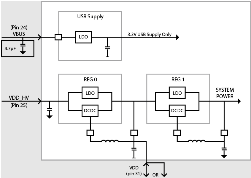
The BL654 power supply system enters one of two supply voltage modes, normal or high voltage mode, depending on how the external supply voltage is connected to these pins.
BL654 power supply options:
- Option 1 – Normal voltage power supply mode entered when the external supply voltage is connected to both the VDD and VDD_HV pins (so that VDD equals VDD_HV). Connect external supply within range 1.7V to 3.6V range to BL654 VDD and VDD_HV pins.
OR - Option 2 – High voltage mode power supply mode (using BL654 VDD_HV pin) entered when the external supply voltage in ONLY connected to the VDD_HV pin and the VDD pin is not connected to any external voltage supply. Connect external supply within range 2.5V to 5.5V range to BL654 VDD_HV pin. BL654 VDD pin left unconnected.
Nordic Errata 197 and 202 related to the use of VDD_HV DCDC convertor, for details refer to http://infocenter.nordicsemi.com/pdf/nRF52840_Rev_1_Errata_v1.1.pdf . Nordic Errata 202 means no external current draw (from VDD pin) is allowed during power up and VDD_HV rise time (to 3V) is below 1mS.
For either option, if you use USB interface then the BL654 VBUS pin must be connected to external supply within the range 4.35V to 5.5V. When using the BL654 VBUS pin, you MUST externally fit a 4.7uF to ground.
BL654 powering options
| Power Supply Pins and Operating Voltage Range | OPTION1 Normal voltage mode operation connect? | OPTION2 High voltage mode operation connect? | OPTION1 with USB peripheral, operation, and normal voltage connect? | OPTION2 with USB peripheral, operation, and high voltage connect? |
|---|---|---|---|---|
| VDD (pin31) 1.7V to 3.6V | Yes (Note 1) | No (Note 2) | Yes | No (Note 2) |
| VDD_HV (pin25) 2.5V to 5.5V | No | Yes | No | Yes (Note 5) |
| VBUS (pin24) 4.35V to 5.5V | No | (Note 3) | Yes (Note 4) | Yes (Note 4) |
Power Supply Option Notes
| Note 1 | Option 1 – External supply voltage is connected to BOTH the VDD and VDD_HV pins (so that VDD equals VDD_HV). Connect external supply within range 1.7V to 3.6V range to BOTH BL654 VDD and VDD_HV pins. | |||||||||||||||||||||||||
| Note 2 | Option 2 – External supply within range 2.5V to 5.5V range to the BL654 VDD_HV pin ONLY. BL654 VDD pin left unconnected. In High voltage mode, the VDD pin becomes an output voltage pin. It can be used to supply external circuitry from the VDD pin. Before any current can be taken from the BL654 VDD pin, this feature must be enabled in the BL654. Additionally, the VDD output voltage is configurable from 1.8V to 3.3V with possible settings of 1.8V, 2.1V, 2.4V, 2.7V, 3.0V, and 3.3V. The default voltage is 1.8V. The supported BL654 VDD pin output voltage range depends on the supply voltage provided on the BL654 VDD_HV pin. The minimum difference between voltage supplied on the VDD_HV pin and the voltage output on the VDD pin is 0.3 V. The maximum output voltage of the VDD pin is VDDH – 0.3V. Table4 shows the current that can be drawn by external circuitry from VDD pin in high voltage mode (supply on VDD_HV). Current that can be drawn by external circuitry from VDD pin in High voltage mode (supply on VDD_HV)
| |||||||||||||||||||||||||
| Note 3 | External current draw is the sum of all GPIO currents and current being drawn from VDD. Depends on whether USB operation is required | |||||||||||||||||||||||||
| Note 4 | When using the BL654 VBUS pin, you must externally fit a 4.7uF capacitor to ground. | |||||||||||||||||||||||||
| Note 5 | To use the BL654 USB peripheral:
When using the BL654 USB peripheral, the VBUS pin can be supplied from same source as VDD_HV (within the operating voltage range of the VBUS pin and VDD_HV pin). |
Low Power Modes
The BL654 has three power modes: Run, Standby Doze, and Deep Sleep.
The module is placed automatically in Standby Doze if there are no pending events (when WAITEVENT statement is encountered within a customer’s smartBASIC script). The module wakes from Standby Doze via any interrupt (such as a received character on the UART Rx line). If the module receives a UART character from either the external UART or the radio, it wakes up.
Deep sleep is the lowest power mode. Once awakened, the system goes through a system reset.
For different Nordic power modes using the Nordic SDK, refer to Nordic infocenter.nordicsemi.com.
Clocks and Timers
Clocks
The integrated high accuracy 32 MHz (±10 ppm) crystal oscillator helps with radio operation and reducing power consumption in the active modes.
The integrated on-chip 32.768 kHz LFRC oscillator (±500 ppm) provides protocol timing and helps with radio power consumption in the system StandByDoze and Deep Sleep modes by reducing the time that the RX window needs to be open.
To keep the on-chip 32.768 kHz LFRC oscillator within ±500 ppm (which is needed to run the BLE stack) accuracy, RC oscillator needs to be calibrated (which takes 33 mS) regularly. The default calibration interval is eight seconds which is enough to keep within ±500 ppm. The calibration interval ranges from 0.25 seconds to 31.75 seconds (in multiples of 0.25 seconds) and configurable via firmware.
Timers
When using smartBASIC, the timer subsystem enables applications to be written which allow future events to be generated based on timeouts.
- Regular Timer – There are eight built-in timers (regular timers) derived from a single RTC clock which are controlled solely by smart BASIC functions. The resolution of the regular timer is 976 microseconds.
- Tick Timer – A 31-bit free running counter that increments every (1) millisecond. The resolution of this counter is 488 microseconds.
Refer to the smart BASIC User Guide available from the Ezurio BL654 product page. For timer utilization when using the Nordic SDK, refer to http://infocenter.nordicsemi.com/index.jsp
Note: Nordic SDK is not supported on the BL654 USB dongle, part #451-00003.
Hardware Architecture
Block Diagrams
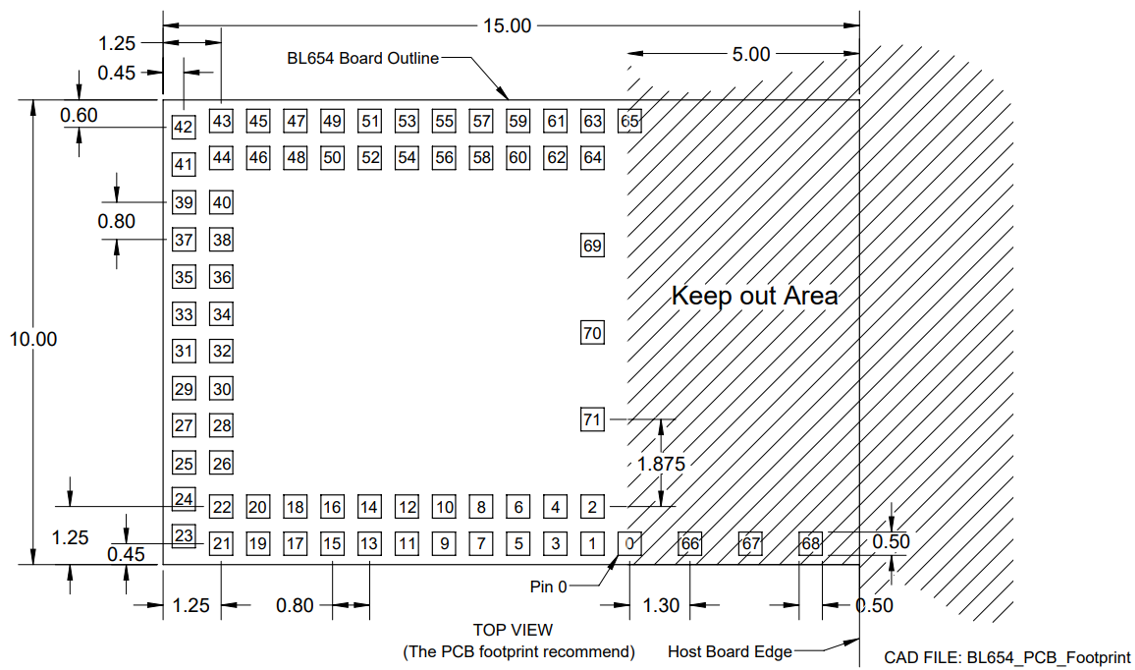
Pin-Out / Package Layout
Mechanical Details
BL654 Mechanical Details
Development Kit Schematics can be found in the software downloads tab of the BL654 product page – https://www.ezurio.com/wireless-modules/bluetooth-modules/bluetooth-5-modules/bl654-series-bluetooth-module-nfc
USB BLE Dongle Mechanical Details
Note: The BL654-US Dongle User Guide is available in the Documentation section of the Ezurio BL654 product page –
https://www.ezurio.com/wireless-modules/bluetooth-modules/bluetooth-5-modules/bl654-series-bluetooth-module-nfc
Pin Definitions & Functionality
| Pin # | Pin Name | Default Function | Alternate Function | In/ Out | Pull Up/ Down | nRF52840 QFN Pin | nRF52840 QFN Name | Comment |
|---|---|---|---|---|---|---|---|---|
| 0 | GND | - | - | - | - | - | - | - |
| 1 | SWDIO | SWDIO | - | IN | PULL-UP | AC24 | SWDIO | - |
| 2 | SIO_36 | SIO_36 | IN | PULL-UP | U24 | P1.04 | - | |
| 3 | SWDCLK | SWDCLK | - | IN | PULL-DOWN | AA24 | SWDCLK | |
| 4 | SIO_34 | SIO_34 | - | - | PULL-UP | W24 | P1.02 | - |
| 5 | SIO_35/ nAutoRUN | nAutoRUN | SIO_35 | IN | PULL-DOWN | V23 | P1.03 | Ezurio Devkit: FTDI USB_DTR via jumper on J12pin1-2. |
| 6 | SIO_33 | SIO_33 | IN | PULL-UP | Y23 | P1.01 | - | |
| 7 | SIO_32 | SIO_32 | - | IN | PULL-UP | AD22 | P1.00 | - |
| 8 | SIO_25 | SIO_25 | - | IN | PULL-UP | AC21 | PO.25 | Ezurio Devkit: BUTTON4 |
| 9 | SIO_23 | SIO_23 | QSPI_DIO3 | IN | PULL-UP | AC19 | PO.23 | - |
| 10 | SIO_24 | SIO_24 | IN | PULL-UP | AD20 | PO.24 | Ezurio Devkit: BUTTON3 | |
| 11 | SIO_22 | SIO_22 | QSPI_DIO2 | IN | PULL-UP | AD18 | PO.22 | - |
| 12 | SIO_21 | SIO_21 | QSPI_DIO1 | IN | PULL-UP | AC17 | PO.21 | - |
| 13 | SIO_20 | SIO_20 | QSPI_DIO0 | IN | PULL-UP | AD16 | PO.20 | - |
| 14 | SIO_19 | SIO_19 | QSPI_CLK | IN | PULL-UP | AC15 | PO.19 | - |
| 15 | D+ | D+ | - | IN | AD6 | D+ | - | |
| 16 | SIO_17 | SIO_17 | QSPI_CS | IN | PULL-UP | AD12 | PO.17 | - |
| 17 | D- | D- | - | IN | AD4 | D- | - | |
| 18 | SIO_15 | SIO_15 | - | IN | PULL-UP | AD10 | PO.15 | Ezurio Devkit: LED3 |
| 19 | nRESET | nRESET | SIO_18 | IN | PULL-UP | AC13 | PO.18 | System Reset (Active Low) |
| 20 | SIO_13 | SIO_13 | - | IN | PULL-UP | AD8 | PO.13 | Ezurio Devkit: LED1 |
| 21 | SIO_16 | SIO_16 | - | IN | PULL-UP | AC11 | PO.16 | Ezurio Devkit: LED4 |
| 22 | SIO_14 | SIO_14 | - | IN | PULL-UP | AC9 | PO.14 | Ezurio Devkit: LED2 |
| 23 | GND | - | - | - | - | - | - | - |
| 24 | VBUS | 4.35V – 5.5V | ||||||
| 25 | VDD_HV | - | - | - | - | - | - | 2.5V to 5.5V |
| 26 | GND | - | - | - | - | - | - | - |
| 27 | SIO_11 | SIO_11 | - | IN | PULL-UP | T2 | PO.11 | Ezurio Devkit: BUTTON1 |
| 28 | SIO_12 | SIO_12 | - | IN | PULL-UP | U1 | PO.12 | BUTTON2 |
| 29 | SIO_08/ UART_RX | SIO_08 | UART_RX | IN | PULL-UP | N1 | PO.08 | UARTCLOSE() selects DIO functionality. UARTOPEN() selects UART COMMS behavior |
| 30 | SIO_41/ SPI_CLK | SIO_41 | SPI_CLK | IN | PULL-UP | R1 | P1.09 | Ezurio Devkit: SPI EEPROM. SPI_Eeprom_CLK, Output: SPIOPEN() in smartBASIC selects SPI function, MOSI and CLK are outputs when in SPI master mode. |
| 31 | VDD | - | - | - | - | 1.7V to 3.6V | ||
| 32 | SIO_40/ SPI_MOSI | SIO_40 | SPI_MOSI | IN | PULL-UP | P2 | P1.08 | Ezurio Devkit: SPI EEPROM. SPI_Eeprom_MOSI, Output SPIOPEN() in smartBASIC selects SPI function, MOSI and CLK are outputs in SPI master. |
| 33 | GND | - | - | - | - | - | - | - |
| 34 | SIO_04/ AIN2/ SPI_MISO | SIO_04 | AIN2/ SPI_MISO | IN | PULL-UP | J1 | PO.04/AIN2 | Ezurio Devkit: SPI EEPROM. SPI_Eeprom_MISO, Input. SPIOPEN() in smartBASIC selects SPI function; MOSI and CLK are outputs when in SPI master mode |
| 35 | SIO_06/ UART_TX | SIO_06 | UART_TX | OUT | Set High in FW | L1 | PO.06 | UARTCLOSE() selects DIO functionality. UARTOPEN() selects UART COMMS behaviour |
| 36 | SIO_26/ I2C_SDA | SIO_26 | I2C_SDA | IN | PULL-UP | G1 | PO.26 | Ezurio Devkit: I2C RTC chip. I2C data line. |
| 37 | SIO_07/ UART_CTS | SIO_07 | UART_CTS | IN | PULL-DOWN | M2 | PO.07 | UARTCLOSE() selects DIO functionality. UARTOPEN() selects UART COMMS behaviour |
| 38 | SIO_27/ I2C_SCL | SIO_27 | I2C_SCL | IN | PULL-UP | H2 | PO.27 | Ezurio Devkit: I2C RTC chip. I2C clock line. |
| 39 | SIO_05/ UART_RTS/ AIN3 | SIO_05 | UART_RTS/ AIN3 | OUT | Set Low in FW | K2 | PO.05/AIN3 | UARTCLOSE() selects DIO functionality. UARTOPEN() selects UART COMMS behaviour |
| 40 | GND | - | - | - | - | - | - | - |
| 41 | SIO_01/ XL2 | SIO_01 | XL2 | IN | PULL-UP | F2 | PO.01/XL2 | Ezurio Devkit: Optional 32.768kHz crystal pad XL2 and associated load capacitor. |
| 42 | SIO_00/ XL1 | SIO_00 | XL1 | IN | PULL-UP | D2 | PO.00/XL1 | Ezurio Devkit: Optional 32.768kHz crystal pad XL1 and associated load capacitor. |
| 43 | GND | - | - | - | - | - | - | - |
| 44 | SIO_31/ AIN7 | SIO_31 | AIN7 | IN | PULL-UP | A8 | PO.31/AIN7 | - |
| 45 | SIO_30/ AIN6 | SIO_30 | AIN6 | IN | PULL-UP | B9 | PO.30/AIN6 | - |
| 46 | SIO_28/ AIN4 | SIO_28 | AIN4 | IN | PULL-UP | B11 | PO.28/AIN4 | - |
| 47 | GND | - | - | - | - | - | - | - |
| 48 | SIO_29/ AIN5 | SIO_29 | AIN5 | IN | PULL-UP | A10 | PO.29/AIN5 | - |
| 49 | SIO_03/ AIN1 | SIO_03 | AIN1 | IN | PULL-UP | B13 | PO.03/AIN1 | Ezurio Devkit: Temp Sens Analog |
| 50 | SIO_02/ AIN0 | SIO_02 | AIN0 | IN | PULL-DOWN | A12 | PO.02/AIN0 | Internal pull-down. Pull High externally to enter VSP (Virtual Serial Port) Service. |
| 51 | SIO_46 | SIO_46 | - | IN | PULL-UP | B15 | P1.14 | - |
| 52 | GND | - | - | - | - | - | - | - |
| 53 | SIO_47 | SIO_47 | - | IN | PULL-UP | A14 | P1.15 | - |
| 54 | SIO_44 | SIO_44 | - | IN | PULL-UP | B17 | P1.12 | Ezurio Devkit: SPI EEPROM. SPI_Eeprom_CS, Input |
| 55 | GND | - | - | - | - | - | - | - |
| 56 | SIO_45 | SIO_45 | - | IN | PULL-UP | A16 | P1.13 | - |
| 57 | NFC2/ SIO_10 | NFC2 | SIO_10 | IN | - | J24 | PO.10/NFC2 | - |
| 58 | GND | - | - | - | - | - | - | - |
| 59 | NFC1/ SIO_09 | NFC1 | SIO_09 | IN | - | L24 | PO.09/NFC1 | - |
| 60 | SIO_43 | SIO_43 | - | IN | PULL-UP | B19 | P1.11 | - |
| 61 | SIO_37 | SIO_37 | - | IN | PULL-UP | T23 | P1.05 | - |
| 62 | SIO_42 | SIO_42 | - | IN | PULL-UP | A20 | P1.10 | - |
| 63 | SIO_38 | N/C | - | IN | PULL-UP | R24 | P1.06 | Reserved for future use. Do not connect. |
| 64 | SIO_39 | SIO_39 | - | IN | PULL-UP | P23 | P1.07 | - |
| 65 | GND | - | - | - | - | - | - | - |
| 66 | GND | - | - | - | - | - | - | - |
| 67 | GND | - | - | - | - | - | - | - |
| 68 | GND | - | - | - | - | - | - | - |
| 69 | GND | - | - | - | - | - | - | - |
| 70 | GND | - | - | - | - | - | - | - |
| 71 | GND | - | - | - | - | - | - | - |
Pin Definition Notes
| Note 1 | SIO = Signal Input or Output. Secondary function is selectable in smartBASIC application or via Nordic SDK. I/O voltage level tracks VDD. AIN = Analog Input. |
| Note 2 | At reset, all SIO lines are configured as the defaults shown above. SIO lines can be configured through the smartBASIC application script to be either inputs or outputs with pull-ups or pull-downs. When an alternative SIO function is selected (such as I2C or SPI), the firmware does not allow the setup of internal pull-up/pull-down. Therefore, when I2C interface is selected, pull-up resistors on I2C SDA and I2C SCL must be connected externally as per I2C standard. |
| Note 3 | JTAG (two-wire SWD interface), pin 1 (SWDIO) and pin 3 (SWDCLK). JTAG is required because Nordic SDK applications can only be loaded using JTAG (smartBASIC firmware can be loaded using the JTAG as well as UART). We recommend that you use JTAG (2-wire interface) to handle future BL654 module smartBASIC firmware upgrades. You MUST wire out the JTAG (2-wire interface) on your host design (see Figure 7, where four lines (SWDIO, SWDCLK, GND and VDD) should be wired out. smartBASIC firmware upgrades can still be performed over the BL654 UART interface, but this is slower (60 seconds using UART vs. 10 seconds when using JTAG) than using the BL654 JTAG (2-wire interface). Upgrading smartBASIC firmware or loading the smartBASIC applications is done using the UART interface. |
| Note 4 | Pull the nRESET pin (pin 19) low for minimum 100 milliseconds to reset the BL654. |
| Note 5 | The SIO_02 pin (pin 50) must be pulled high externally to enable VSP (Virtual Serial Port) which would allow OTA (over-the-air) smartBASIC application download. Refer to the latest firmware release documentation for details. |
| Note 6 | Ensure that SIO_02 (pin 50) and AutoRUN (pin 5) are not both high (externally), in that state, the UART is bridged to Virtual Serial Port service; the BL654 module does not respond to AT commands and cannot load smartBASIC application scripts. |
| Note 7 | Pin 5 (nAutoRUN) is an input, with active low logic. In the development kit it is connected so that the state is driven by the host’s DTR output line. The nAutoRUN pin must be externally held high or low to select between the following two BL654 operating modes:
The smartBASIC firmware checks for the status of nAutoRUN during power-up or reset. If it is low and if there is a smartBASIC application script named $autorun$, then the smartBASIC firmware executes the application script automatically; hence the name Self-contained Run Mode. |
| Note 8 | The smartBASIC firmware has SIO pins as Digital (Default Function) INPUT pins, which are set PULL-UP by default. This avoids floating inputs (which can cause current consumption to drive with time in low power modes (such as Standby Doze). You can disable the PULL-UP through your smartBASIC application. All of the SIO pins (with a default function of DIO) are inputs (apart from SIO_05 and SIO_06, which are outputs):
|
| Note 9 | BL654 also allows as an option to connect an external higher accuracy (±20 ppm) 32.768 kHz crystal to the BL654 pins SIO_01/XL2 (pin 41) and SIO_00/XL1 (pin 42). This provides higher accuracy protocol timing and helps with radio power consumption in the system standby doze/deep sleep modes by reducing the time that the Rx window must be open. |
| Note 10 | Not required for BL654 module normal operation. The on-chip 32.768kHz LFRC oscillator provides the standard accuracy of ±500 ppm, with calibration required every 8seconds (default) to stay within ±500 ppm. BL654 power supply options:
Nordic Errata 197 and 202 related to the use of VDD_HV DCDC convertor, for details refer to http://infocenter.nordicsemi.com/pdf/nRF52840_Rev_1_Errata_v1.1.pdf. Nordic Errata 202 means no external current draw (from VDD pin) is allowed during power up and VDD_HV rise time (to 3V) is below one millisecond.
|
Electrical Characteristics
Absolute Maximum Ratings
Absolute maximum ratings for supply voltage and voltages on digital and analogue pins of the module are listed below; exceeding these values causes permanent damage.
Maximum current ratings
| Parameter | Min | Max | Unit |
|---|---|---|---|
| Voltage at VDD pin | -0.3 | +3.9 (Note 1) | V |
| Voltage at VDD_HV pin | -0.3 | +5.8 | V |
| VBUS | -0.3 | +5.8 | V |
| Voltage at GND pin | 0 | V | |
| Voltage at SIO pin (at VDD≤3.6V) | -0.3 | VDD +0.3 | V |
| Voltage at SIO pin (at VDD≥3.6V) | -0.3 | 3.9 | V |
| NFC antenna pin current (NFC1/2) | - | 80 | mA |
| Radio RF input level | - | 10 | dBm |
| Environmental | |||
| Storage temperature | -40 | +85 | ºC |
| MSL (Moisture Sensitivity Level) | - | 4 | - |
ESD (as per EN301-489) Conductive Air Coupling | 4 8 | KV KV | |
| Flash Memory (Endurance) (Note 2) | - | 10000 | Write/erase cycles |
| Flash Memory (Retention) | - | 10 years at 40°C | - |
Maximum Ratings Notes
| Note 1 | The absolute maximum rating for VDD_nRF pin (max) is 3.9V for the BL654. |
| Note 2 | Wear levelling is used in file system. |
Recommended Operating Conditions
Power Supply Operating Parameters
| Parameter | Min | Typ | Max | Unit |
|---|---|---|---|---|
| VDD (independent of DCDC)1 supply range | 1.7 | 3.3 | 3.6 | V |
| VDD_HV (independent of DCDC) supply range | 2.5 | 3.7 | 5.5 | V |
| VBUS USB supply range | 4.35 | 5 | 5.5 | V |
| VDD Maximum ripple or noise2 | - | - | 10 | mV |
| VDD supply rise time (0V to 1.7V)3 Time in Power | - | - | 60 | mS mS mS mS |
| VDD_HV supply rise time (0V to 3.7V) 3 | 100 | mS | ||
| Operating Temperature Range | -40 | - | +85 | ºC |
Recommended Power Supply Operating Parameter Notes
| Note 1 | 4.7 uF internal to module on VDD. The internal DCDC convertor or LDO is decided by the underlying BLE stack. |
| Note 2 | This is the maximum VDD or VDD_HV ripple or noise (at any frequency) that does not disturb the radio. |
| Note 3 | The on-board power-on reset circuitry may not function properly for rise times longer than the specified maximum. |
| Note 4 | BL654 power supply options:
|
Signal Levels and Interface Specs
Signal Levels for Inferface, SIO
| Parameter | Min | Typ | Max | Unit |
|---|---|---|---|---|
| VIH Input high voltage | 0.7 VDD | VDD | V | |
| VIL Input low voltage | VSS | 0.3 x VDD | V | |
VOH Output high voltage (std. drive, 0.5mA) (Note 1) (high-drive, 3mA) (Note 1) (high-drive, 5mA) (Note 2) | VDD -0.4 VDD -0.4 VDD -0.4 | VDD VDD VDD | V V | |
| VOL Output low voltage (std. drive, 0.5mA) (Note 1) (high-drive, 3mA) (Note 1) (high-drive, 5mA) (Note 2) | VSS VSS VSS | VSS+0.4 VSS+0.4 VSS+0.4 | V V | |
| VOL Current at VSS+0.4V, Output set low (std. drive, 0.5mA) (Note 1) (high-drive, 3mA) (Note 1) (high-drive, 5mA) (Note 2) | 1 3 6 | 2 - 10 | 4 - 15 | mA mA mA |
| VOL Current at VDD -0.4, Output set low (std. drive, 0.5mA) (Note 1) (high-drive, 3mA) (Note 1) (high-drive, 5mA) (Note 2) | 1 3 6 | 2 - 9 | 4 - 14 | mA mA mA |
| Pull up resistance | 11 | 13 | 16 | kΩ |
| Pull down resistance | 11 | 13 | 16 | kΩ |
| Pad capacitance | 3 | pF | ||
| Pad capacitance at NFC pads | 4 | pF |
Signal Levels Notes:
| Note 1 | For VDD≥1.7V. The firmware supports high drive (3 mA, as well as standard drive). |
| Note 2 | For VDD≥2.7V. The firmware supports high drive (5 mA (since VDD≥2.7V), as well as standard drive). The GPIO (SIO) high reference voltage always equals the level on the VDD pin.
|
SIO Pin Alternative Function AIN (ADC) Specification
| Parameter | Min | Typ | Max | Unit | ||||
|---|---|---|---|---|---|---|---|---|
| Maximum sample rate | 200 | kHz | ||||||
| ADC Internal reference voltage | -1.5% | 0.6 V | +1.5% | % | ||||
ADC pin input internal selectable scaling | 4, 2, 1, 1/2, 1/3, 1/4, 1/5 1/6 | scaling | ||||||
ADC input pin (AIN) voltage maximum without damaging ADC w.r.t (see Note 1)
| VDD+0.3 | V | ||||||
| Configurable Resolution | 8-bit mode | 10-bit mode | 12-bit mode | bits | ||||
| Configurable (see Note 2) Acquisition Time, source resistance ≤10kΩ Acquisition Time, source resistance ≤40kΩ Acquisition Time, source resistance ≤100kΩ Acquisition Time, source resistance ≤200kΩ Acquisition Time, source resistance ≤400kΩ Acquisition Time, source resistance ≤800kΩ | 3 5 10 15 20 40 | uS uS uS uS uS uS | ||||||
| Conversion Time (see Note 3) | <2 | uS | ||||||
| ADC input impedance (during operation) (see Note 3) Input Resistance Sample and hold capacitance at maximum gain | >1 2.5 | MOhm pF |
Recommended Operating Parameters Notes
| Note 1 | Stay within internal 0.6 V reference voltage with given pre-scaling on AIN pin and do not violate ADC maximum input voltage (for damage) for a given VCC, e.g. If VDD is 3.6V, you can only expose AIN pin to VDD+0.3 V. Default pre-scaling is 1/6 which configurable via smartBASIC. |
| Note 2 | Firmware allows configurable resolution (8-bit, 10-bit or 12-bit mode) and acquisition time. BL654 ADC is a Successive Approximation type ADC (SSADC), as a result no external capacitor is needed for ADC operation. Configure the acquisition time according to the source resistance that customer has. The sampling frequency is limited by the sum of sampling time and acquisition time. The maximum sampling time is 2us. For acquisition time of 3us the total conversion time is therefore 5us, which makes maximum sampling frequency of 1/5us = 200kHz. Similarly, if acquisition time of 40us chosen, then the conversion time is 42us and the maximum sampling frequency is 1/42us = 23.8kHz. |
| Note 3 | ADC input impedance is estimated mean impedance of the ADC (AIN) pins. |
Power Management & Consumption
Power Consumption
Data at VDD of 3.3 V with internal (to chipset) LDO ON or with internal (to chipset) DCDC ON (see Power Consumption Note 1) and 25ºC.
| Parameter | Min | Typ | Max | Unit |
|---|---|---|---|---|
| Active mode ‘peak’ current (Note 1) (Advertising or Connection) | With DCDC [with LDO] | |||
| Tx only run peak current @ Txpwr = +8 dBm | 14.8 [32.7] | mA | ||
| Tx only run peak current @ Txpwr = +4 dBm | 9.6 [21.4] | mA | ||
| Tx only run peak current @ Txpwr = 0 dBm | 4.8 [10.6] | mA | ||
| Tx only run peak current @ Txpwr = -4 dBm | 3.1 [8.1] | mA | ||
| Tx only run peak current @ Txpwr = -8 dBm | 3.3 [7.2] | mA | ||
| Tx only run peak current @ Txpwr = -12 dBm | 3.0 [6.4] | mA | ||
| Tx only run peak current @ Txpwr = -16 dBm | 2.8 [6.0] | mA | ||
| Tx only run peak current @ Txpwr = -20 dBm | 2.7 [5.6] | mA | ||
| Tx only run peak current @ Txpwr = -40 dBm | 2.3 [4.6] | mA | ||
| Active Mode | ||||
| Active Mode – Rx only ‘peak’ current, BLE 1 Mbps (Note 1) | 4.6 [9.9] | mA | ||
| Active Mode – Rx only ‘peak’ current, BLE 2 Mbps (Note 2) | 5.2 [11.1] | mA | ||
| Ultra-Low Power Mode | ||||
| Ultra-Low Power Mode 1 (Note 2) Standby Doze, 256k RAM retention | 3.1 | µA | ||
| Ultra-Low Power Mode 2 (Note 3) Deep Sleep (no RAM retention) | 0.4 | µA | ||
| Active Mode Average current (Note 4) Advertising Average Current draw | ||||
| Max, with advertising interval (min) 20 ms | Note 4 | µA | ||
| Min, with advertising interval (max) 10240 ms | Note 4 | µA | ||
| Connection Average Current draw | ||||
| Max, with connection interval (min) 7.5 ms | Note 4 | µA | ||
| Min, with connection interval (max) 4000 ms | Note 4 | µA | ||
| Note 1 | This is for Peak Radio Current only, but there is additional current due to the MCU. The internal DCDC convertor or LDO is decided by the underlying BLE stack. |
| Note 2 | BL654 modules Standby Doze is 3.1 uA typical. When using smartBASIC firmware, Standby Doze is entered automatically (when a waitevent statement is encountered within a smartBASIC application script). In Standby Doze, all peripherals that are enabled stay on and may re-awaken the chip. Depending on active peripherals, current consumption ranges from 3.1 μA to 370 uA (when UART is ON). See individual peripherals current consumption data in the Peripheral Block Current Consumption section. smartBASIC firmware has functionality to detect GPIO change with no current consumption cost, it is possible to close the UART and get to the 3.1 uA current consumption regime and still be able to detect for incoming data and be woken up so that the UART can be re-opened at expense of losing that first character. The BL654 Standby Doze current consists of the below nRF52840 blocks:
|
| Note 3 | In Deep Sleep, everything is disabled and the only wake-up sources (including NFC to wakeup) are reset and changes on SIO or NFC pins on which sense is enabled. The current consumption seen is ~0.4 uA typical in BL654 modules.
|
| Note 4 | Average current consumption depends on several factors (including Tx power, VCC, accuracy of 32MHz and 32.768 kHz). With these factors fixed, the largest variable is the advertising or connection interval set. Advertising Interval range:
For an advertising event:
Other factors that are also related to average current consumption include the advertising payload bytes in each advertising packet and whether it’s continuously advertising or periodically advertising. Connection Interval range (for a peripheral):
For a connection event (for a peripheral device):
Other factors that are also related to average current consumption include:
Connection Interval range (for a central device):
|
Peripheral Block Power Consumption
The values below are calculated for a typical operating voltage of 3V.
UART Power Consumption
| Parameter | Min | Typ | Max | Unit | |
|---|---|---|---|---|---|
| WITH DCDC(REG1) | WITH LDO(REG1) | ||||
| UART Run current @ 115200 bps | - | 729 | 951 | - | uA |
| UART Run current @ 1200 bps | - | 729 | 951 | - | uA |
| Idle current for UART (no activity) | - | 29 | 29 | - | uA |
| UART Baud rate | 1.2 | - | 1000 | kbps | |
SPI Power Consumption
| Parameter | Min | Typ | Max | Unit | |
|---|---|---|---|---|---|
| with DCDC(REG1) | with LDO(REG1) | ||||
| SPI Master Run current @ 2 Mbps | - | 803 | 1040 | - | uA |
| SPI Master Run current @ 8 Mbps | - | 803 | 1040 | - | uA |
| Idle current for SPI (no activity) | - | <1 | <1 | - | uA |
| SPI bit rate | - | - | 8 | Mbps | |
I2C Power Consumption
| Parameter | Min | Typ | Max | Unit | |
|---|---|---|---|---|---|
| with DCDC(REG1) | with LDO(REG1) | ||||
| I2C Run current @ 100 kbps | - | 967 | 1250 | - | uA |
| I2C Run current @ 400 kbps | - | 967 | 1250 | - | uA |
| Idle current for I2C (no activity) | - | 3.2 | 3.2 | - | uA |
| I2C Bit rate | 100 | - | 400 | kbps | |
ADC Power Consumption
| Parameter | Min | Typ | Max | Unit | |
|---|---|---|---|---|---|
| with DCDC(REG1) | with LDO(REG1) | ||||
| ADC current during conversion | - | 1640 | 2010 | - | uA |
| Idle current for ADC (no activity) | - | 0 | 0 | - | uA |
RF, Antenna, and Wireless Details
451-00001 On-Board PCB Antenna Characteristics
The 451-00001 on-board PCB trace monopole antenna radiated performance depends on the host PCB layout.
The BL654 development board was used for BL654 development and the 451-00001 PCB antenna performance evaluation. To obtain similar performance, follow guidelines in section PCB Layout on Host PCB for the 451-00001 to allow the on-board PCB antenna to radiate and reduce proximity effects due to nearby host PCB GND copper or metal covers.
Notes:
Antenna P = Antenna input power (set).
TRP = Total Radiated Power (measured).
EIRP = Equivalent Isotropic (ideal) Radiated Power (measured).
Efficiency = TRP - Antenna P (calculated).
Gain = Max. EIRP - Antenna P (calculated).

2402MHz Radiated Performance
EIRP Azimuth Cut
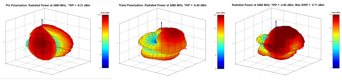
3D Plots:
2440MHz Radiated Performance
EIRP Azimuth Cut
3D Plots:
2480MHz Radiated Performance
EIRP Azimuth Cut
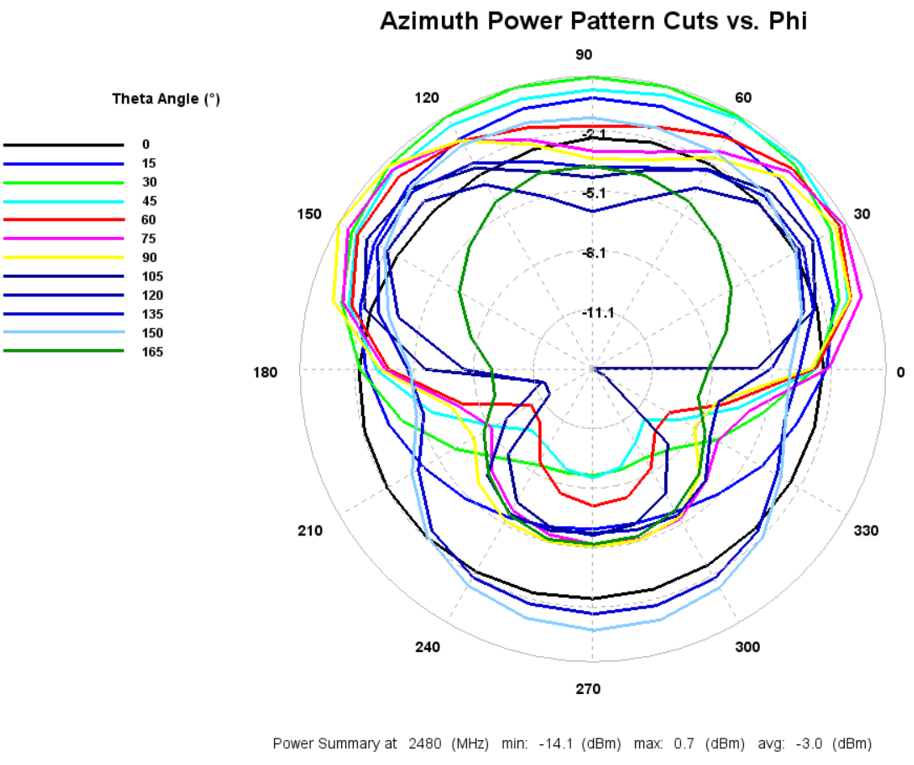
3D Plots:
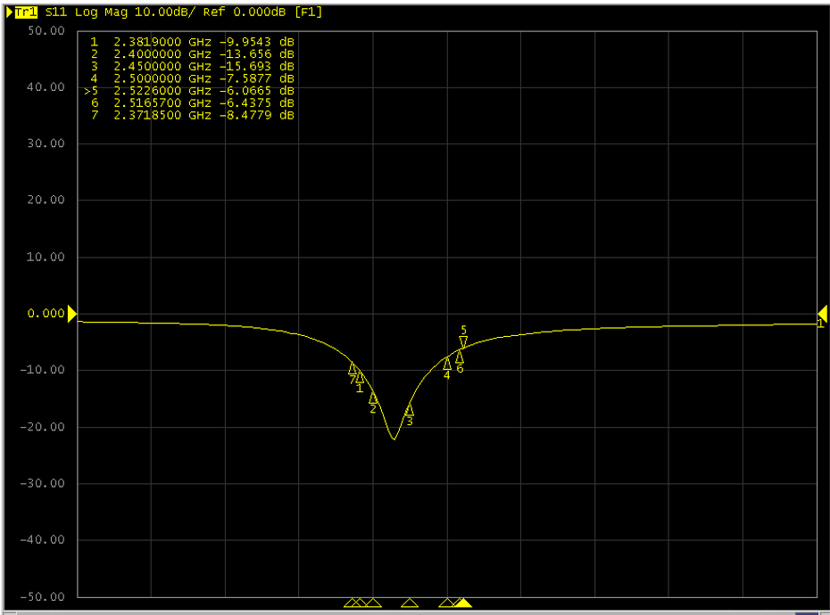
451-00001 Return Loss Measurement
Integration Guidelines
Circuit
The BL654 is easy to integrate, requiring no external components on your board apart from those which you require for development and in your end application.
The following are suggestions for your design for the best performance and functionality.
Checklist (for Schematic):
- BL654 power supply options:
Option 1 – Normal voltage power supply mode entered when the external supply voltage is connected to both the VDD and VDDH pins (so that VDD equals VDD_HV). Connect external supply within range 1.7V to 3.6V range to BL654 VDD and VDD_HV pins.
OR
Option 2 – High voltage mode power supply mode (using BL654 VDD_HV pin) entered when the external supply voltage in ONLY connected to the VDDH pin and the VDD pin is not connected to any external voltage supply. Connect external supply within range 2.5V to 5.5V range to BL654 VDD_HV pin. BL654 VDD pin left unconnected.
Nordic Errata 197 and 202 related to the use of VDD_HV DCDC convertor, for details refer to http://infocenter.nordicsemi.com/pdf/nRF52840_Rev_1_Errata_v1.1.pdf. Nordic Errata 202 means no external current draw (from VDD pin) is allowed during power up and VDD_HV rise time (to 3V) is below 1mS.
For either option, if you use USB interface then the BL654 VBUS pin must be connected to external supply within the range 4.35V to 5.5V. When using the BL654 VBUS pin, you MUST externally fit a 4.7uF to ground.
External power source should be within the operating range, rise time and noise/ripple specification of the BL654. Add decoupling capacitors for filtering the external source. Power-on reset circuitry within BL654 series module incorporates brown-out detector, thus simplifying your power supply design. Upon application of power, the internal power-on reset ensures that the module starts correctly. - VDD and coin-cell operation
With a built-in DCDC (operating range 1.7V to 3.6V), that reduces the peak current required from a coin-cell, making it easier to use with a coin-cell. - AIN (ADC) and SIO pin IO voltage levels
BL654 SIO voltage levels are at VDD. Ensure input voltage levels into SIO pins are at VDD also (if VDD source is a battery whose voltage will drop). Ensure ADC pin maximum input voltage for damage is not violated. - AIN (ADC) impedance and external voltage divider setup
If you need to measure with ADC a voltage higher than 3.6V, you can connect a high impedance voltage divider to lower the voltage to the ADC input pin. - JTAG
This is REQUIRED as Nordic SDK applications can only be loaded using the JTAG (smartBASIC firmware can be loaded using the JTAG as well as the UART).
Ezurio recommends you use JTAG (2-wire interface) to handle future BL654 module firmware upgrades. You MUST wire out the JTAG (2-wire interface) on your host design (see Figure 7, where four lines should be wired out, namely SWDIO, SWDCLK, GND and VCC). Firmware upgrades can still be performed over the BL654 UART interface, but this is slower (60 seconds using UART vs. 10 seconds when using JTAG) than using the BL654 JTAG (2-wire interface).
JTAG may be used if you intend to use Flash Cloning during production to load smartBASIC scripts. - UART
Required for loading your smartBASIC application script during development (or for subsequent firmware upgrades (except JTAG for FW upgrades and/or Flash Cloning of the smartBASIC application script). Add connector to allow interfacing with UART via PC (UART–RS232 or UART-USB). - UART_RX and UART_CTS
SIO_08 (alternative function UART_RX) is an input, set with internal weak pull-up (in firmware). The pull-up prevents the module from going into deep sleep when UART_RX line is idling.
SIO_07 (alternative function UART_CTS) is an input, set with internal weak pull-down (in firmware). This pull-down ensures the default state of the UART_CTS will be asserted which means can send data out of the UART_TX line. Ezurio recommends that UART_CTS be connected. nAutoRUN pin and operating mode selection
nAutoRUN pin needs to be externally held high or low to select between the two BL654 operating modes at power-up:- Self-contained Run mode (nAutoRUN pin held at 0V).
- Interactive / development mode (nAutoRUN pin held at VDD).
Make provision to allow operation in the required mode. Add jumper to allow nAutoRUN pin to be held high or low (BL654 has internal 13K pull-down by default) OR driven by host GPIO.
- I2C
It is essential to remember that pull-up resistors on both I2C_SCL and I2C_SDA lines are not provided in the BL654 module and MUST be provided external to the module as per I2C standard. - SPI
Implement SPI chip select using any unused SIO pin within your smartBASIC application script or Nordic application then SPI_CS is controlled from the software application allowing multi-dropping. - SIO pin direction
BL654 modules shipped from production with smart BASIC FW, all SIO pins (with default function of DIO) are mostly digital inputs (see Pin Definitions Table2). Remember to change the direction SIO pin (in your smartBASIC application script) if that particular pin is wired to a device that expects to be driven by the BL654 SIO pin configured as an output. Also, these SIO pins have the internal pull-up or pull-down resistor-enabled by default in firmware (see Pin Definitions Table 2). This was done to avoid floating inputs, which can cause current consumption in low power modes (e.g. StandbyDoze) to drift with time. You can disable the PULL-UP or Pull-down through their smartBASIC application.
Note: Internal pull-up, pull down will take current from VDD. - SIO_02 pin and OTA smartBASIC application download feature
SIO_02 is an input, set with internal pull-down (in FW). Refer to latest firmware release documentation on how SIO_02 is used for Over the Air smartBASIC application download feature. The SIO_02 pin must be pulled high externally to enable the feature. Decide if this feature is required in production. When SIO_02 is high, ensure nAutoRun is NOT high at same time; otherwise you cannot load the smartBASIC application script. NFC antenna connector
To make use of the Ezurio flexi-PCB NFC antenna, fit connector:- Description – FFC/FPC Connector, Right Angle, SMD/90d, Dual Contact,1.2 mm Mated Height
- Manufacturer – Molex
- Manufacturers Part number – 512810594
- Add tuning capacitors of 300 pF on NFC1 pin to GND and 300 pF on NFC2 pins to GND if the PCB track length is similar as development board.
- nRESET pin (active low)
Hardware reset. Wire out to push button or drive by host.
By default module is out of reset when power applied to VCC pins. - Optional External 32.768kHz crystal
If the optional external 32.768kHz crystal is needed then use a crystal that meets specification and add load capacitors whose values should be tuned to meet all specification for frequency and oscillation margin. - SIO_38 special function pin
This is for future use by Ezurio. It is currently a Do Not Connect pin if using the smartBASIC FW.
PCB Layout
PCB Layout on Host PCB - General
Checklist (for PCB):
- MUST locate BL654 module close to the edge of PCB (mandatory for the 451-00001 for on-board PCB trace antenna to radiate properly).
- Use solid GND plane on inner layer (for best EMC and RF performance).
- All module GND pins MUST be connected to host PCB GND.
- Place GND vias close to module GND pads as possible.
- Unused PCB area on surface layer can flooded with copper but place GND vias regularly to connect the copper flood to the inner GND plane. If GND flood copper is on the bottom of the module, then connect it with GND vias to the inner GND plane.
- Route traces to avoid noise being picked up on VDD, VDDH, VBUS supply and AIN (analogue) and SIO (digital) traces.
- Ensure no exposed copper is on the underside of the module (refer to land pattern of BL654 development board).
PCB Layout on Host PCB for the 451-00001
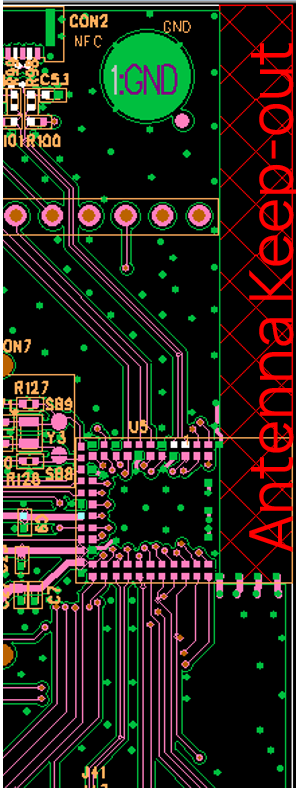
Host PCB Land Pattern and Antenna Keep-Out for the 451-00001 Notes
| Note 1 | Ensure there is no copper in the antenna ‘keep out area’ on any layers of the host PCB. Also keep all mounting hardware or any metal clear of the area (Refer to 6.3.2) to reduce effects of proximity detuning the antenna and to help antenna radiate properly. |
| Note 2 | For the best on-board antenna performance, the module 451-00001 MUST be placed on the edge of the host PCB and preferably in the edge centre and host PCB, the antenna “Keep Out Area” is extended (see Note 4). |
| Note 3 | BL654 development board has the 451-00001 placed on the edge of the PCB board (and not in corner) for that the Antenna keep out area is extended down to the corner of the development board, see section PCB Layout on Host PCB for the 451-00001, Figure 18. This was used for module development and antenna performance evaluation. |
| Note 4 | Ensure that there is no exposed copper under the module on the host PCB. |
| Note 5 | You may modify the PCB land pattern dimensions based on their experience and/or process capability. |
Antenna Keep-Out on Host PCB
The 451-00001 has an integrated PCB trace antenna and its performance is sensitive to host PCB. It is critical to locate the 451-00001 on the edge of the host PCB (or corner) to allow the antenna to radiate properly. Refer to guidelines in section PCB land pattern and antenna keep-out area for the 451-00001. Some of those guidelines repeated below.
- Ensure there is no copper in the antenna keep-out area on any layers of the host PCB. Keep all mounting hardware and metal clear of the area to allow proper antenna radiation.
- For best antenna performance, place the 451-00001 module on the edge of the host PCB, preferably in the edge center.
- The BL654 development board has the 451-00001 module on the edge of the board (not in the corner). The antenna keep-out area is defined by the BL654 development board which was used for module development and antenna performance evaluation is shown in Figure 14, where the antenna keep-out area is ~5 mm wide, ~39.95 mm long; with PCB dielectric (no copper) height ~1 mm sitting under the 451-00001 PCB trace antenna.
- The 451-00001 PCB trace antenna is tuned when the 451-00001 is sitting on development board (host PCB) with size of 125 mm x 85 mm x 1mm.
- A different host PCB thickness dielectric will have small effect on antenna.
- The antenna-keep-out defined in the Host PCB Land Pattern and Antenna Keep-out for the 451-00001 section.
Host PCB land pattern and antenna keep-out for the BL654 applies when the 451-00001 is placed in the edge of the host PCB preferably in the edge center
Antenna Keep-Out Notes:
| Note 1 | The BL654 module is placed on the edge, preferably edge centre of the host PCB. |
| Note 2 | Copper cut-away on all layers in the Antenna Keep-out area under the 451-00001 on host PCB. |
Antenna Keep-Out and Proximity to Metal or Plastic
Checklist (for metal /plastic enclosure):
- Minimum safe distance for metals without seriously compromising the antenna (tuning) is 40 mm top/bottom and 30 mm left or right.
- Metal close to the 451-00001 PCB trace monopole antenna (bottom, top, left, right, any direction) will have degradation on the antenna performance. The amount of that degradation is entirely system dependent, meaning you will need to perform some testing with your host application.
- Any metal closer than 20 mm will begin to significantly degrade performance (S11, gain, radiation efficiency).
- It is best that you test the range with a mock-up (or actual prototype) of the product to assess effects of enclosure height (and materials, whether metal or plastic).
External Antenna Integration with the 451-00002
Please refer to the regulatory sections for FCC, ISED, EU, and Japan for details of use of BL654-with external antennas in each regulatory region.
The BL654 family has been designed to operate with the below external antennas (with a maximum gain of
2.0 dBi). The required antenna impedance is 50 ohms. See Table 27. External antennas improve radiation efficiency.
Note: EFG2400A3S is for FCC/IC only.
External antennas for the BL654
| Manufacturer | Model | Ezurio Part Number | Type | Connector | Peak Gain | |
|---|---|---|---|---|---|---|
| 2400-2500 MHz | 2400-2480 MHz | |||||
| Ezurio (Laird Connectivity) | NanoBlue | EBL2400A1-10MH4L | PCB Dipole | IPEX MHF4 | 2 dBi | - |
| Ezurio (Laird Connectivity) | FlexPIFA | 001-0022 | PIFA | IPEX MHF4 | - | 2 dBi |
| Ezurio (Laird Connectivity) | FlexNotch | 001-0023 | Notch | IPEX MHF4 | - | 2 dBi |
| Mag.Layers | EDA-8709-2G4C1-B27-CY | 0600-00057 | Dipole | IPEX MHF4 | 2 dBi | - |
| Ezurio (Laird Connectivity) | mFlexPIFA | EFA2400A3S-10MH4L | PIFA | IPEX MHF4 | - | 2 dBi |
| Ezurio (Laird Connectivity) | Ezurio NFC | 0600-00061 | NFC | N/A | - | - |
| Walsin | RFDPA870900SBAB8G1 | NA | Dipole | SMA | 2dBi | |
| Ezurio (Laird Connectivity) | i-FlexPIFA | EFG2400A3S | Flexible PIFA | MHF1/MHF4 | 3.1 dBi | |
Application Note for Surface Mount Modules
Introduction
Ezurio surface mount modules are designed to conform to all major manufacturing guidelines. This application note is intended to provide additional guidance beyond the information that is presented in the User Manual. This Application Note is considered a living document and will be updated as new information is presented.
The modules are designed to meet the needs of several commercial and industrial applications. They are easy to manufacture and conform to current automated manufacturing processes.
Shipping
Tape and Reel Packaging
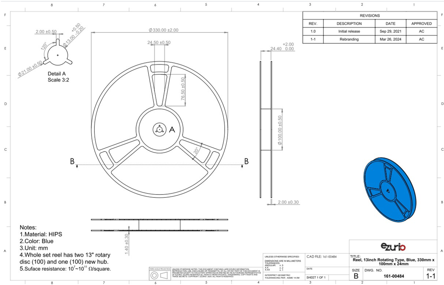
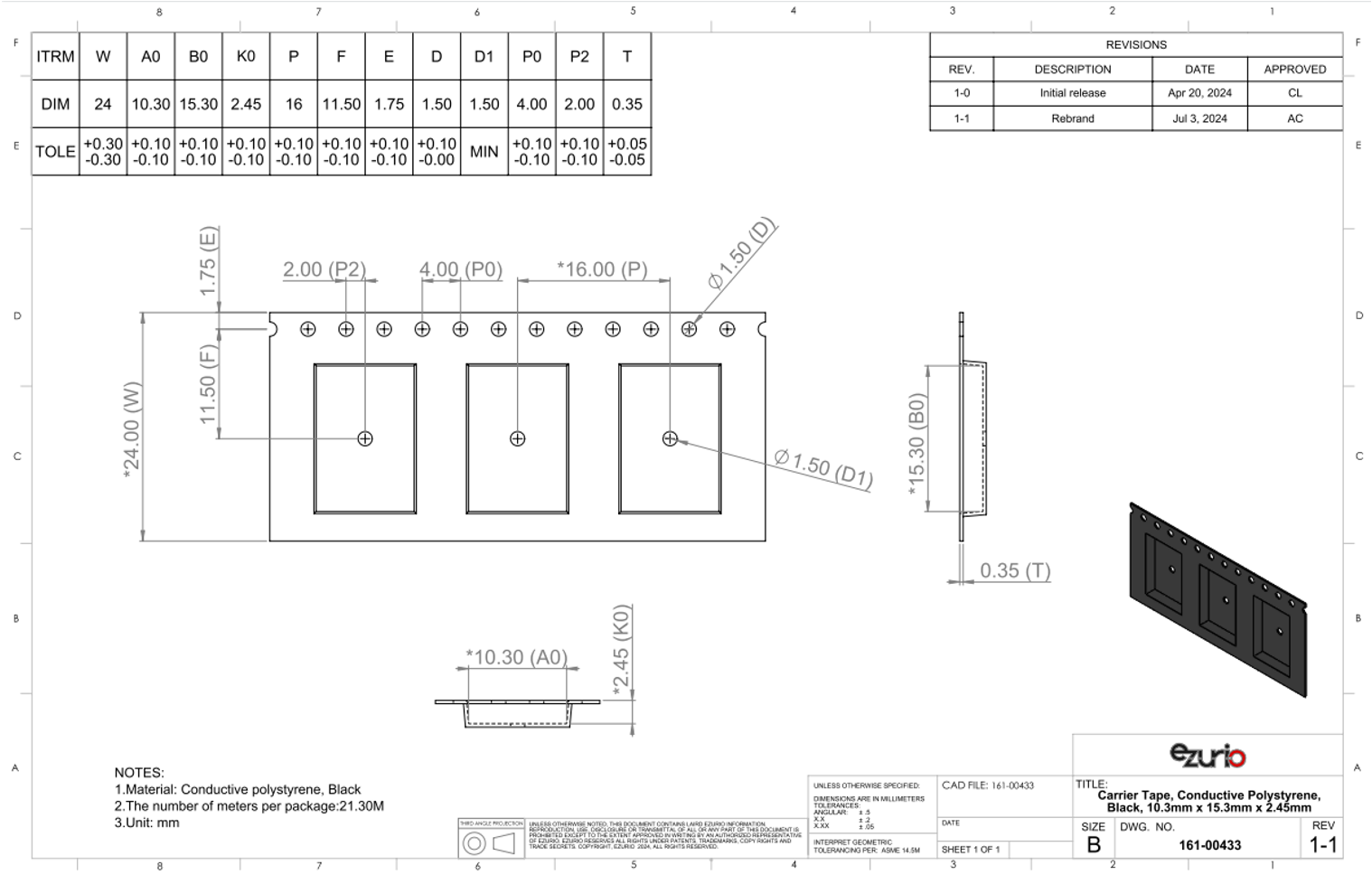
There are 1,000 x BL654 modules taped in a reel (and packaged in a pizza box) and five boxes per carton (5000 modules per carton). Reel, boxes, and carton are labeled with the appropriate labels. See Carton Contents for more information.
Carton Contents
The following are the contents of the carton shipped for the BL654 modules.
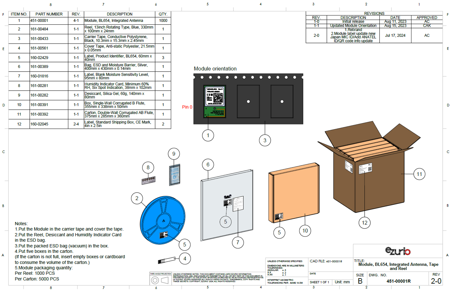
Module Orientation in Cavity
Labeling
The following package label is located on the box:
The following package label is located on the adjacent sides of the master carton:
Reflow Parameters
Prior to any reflow, it is important to ensure the modules were packaged to prevent moisture absorption. New packages contain desiccate (to absorb moisture) and a humidity indicator card to display the level maintained during storage and shipment. If directed to bake units on the card, see Table 28 and follow instructions specified by IPC/JEDEC J-STD-033. A copy of this standard is available from the JEDEC website: http://www.jedec.org/sites/default/files/docs/jstd033b01.pdf
Any modules not manufactured before exceeding their floor life should be re-packaged with fresh desiccate and a new humidity indicator card. Floor life for MSL (Moisture Sensitivity Level) four devices is 72 hours in ambient environment £30°C/60%RH.
Recommended baking times and temperatures
| MSL | 125°C Baking Temp. | 90°C/≤ 5%RH Baking Temp. | 40°C/ ≤ 5%RH Baking Temp. | |||
|---|---|---|---|---|---|---|
| Saturated @ 30°C/85% | Floor Life Limit + 72 hours @ 30°C/60% | Saturated @ 30°C/85% | Floor Life Limit + 72 hours @ 30°C/60% | Saturated @ 30°C/85% | Floor Life Limit + 72 hours @ 30°C/60% | |
| 4 | 11 hours | 7 hours | 37 hours | 23 hours | 15 days | 9 days |
Ezurio surface mount modules are designed to be easily manufactured, including reflow soldering to a PCB. Ultimately it is the responsibility of the customer to choose the appropriate solder paste and to ensure oven temperatures during reflow meet the requirements of the solder paste. Ezurio surface mount modules conform to J-STD-020D1 standards for reflow temperatures.
Important: During reflow, modules should not be above 260° and not for more than 30 seconds. In addition, we recommend that the BL654 module does not go through the reflow process more than one time; otherwise, the BL654 internal component soldering may be impacted.
Temperatures should not exceed the minimums or maximums presented below.
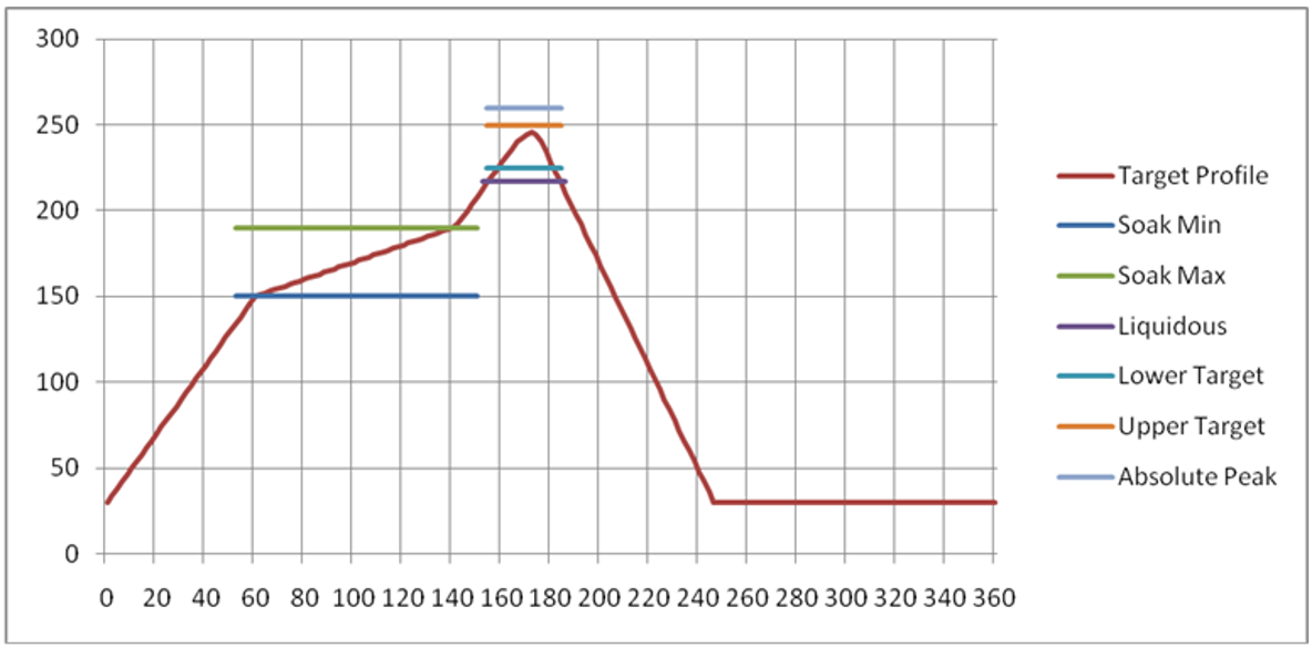
Recommended maximum and minimum temperatures
| Specification | Value | Unit |
|---|---|---|
| Temperature Inc./Dec. Rate (max) | 1~3 | °C / Sec |
| Temperature Decrease rate (goal) | 2-4 | °C / Sec |
| Soak Temp Increase rate (goal) | .5 - 1 | °C / Sec |
| Flux Soak Period (Min) | 70 | Sec |
| Flux Soak Period (Max) | 120 | Sec |
| Flux Soak Temp (Min) | 150 | °C |
| Flux Soak Temp (max) | 190 | °C |
| Time Above Liquidous (max) | 70 | Sec |
| Time Above Liquidous (min) | 50 | Sec |
| Time In Target Reflow Range (goal) | 30 | Sec |
| Time At Absolute Peak (max) | 5 | Sec |
| Liquidous Temperature (SAC305) | 218 | °C |
| Lower Target Reflow Temperature | 240 | °C |
| Upper Target Reflow Temperature | 250 | °C |
| Absolute Peak Temperature | 260 | °C |
Environmental and Reliability
Environmental Requirements
Reliability Tests
The BL654 module went through the below reliability tests and passed.
| Test Sequence | Test Item | Test Limits and Pass | Test Conditions |
|---|---|---|---|
| 1 | Vibration Test | JESD22-B103B Vibration, Variable frequency | Sample: Unpowered. Sample number: 3. Vibration waveform: Sine waveform. Vibration frequency /Displacement: 20 to 80Hz /1.52mm. Vibration frequency /Acceleration: 80 to 2000Hz /20g. Cycle time: 4 minutes. Number of cycles: 4 cycles for each axis. Vibration axis: X, Y and Z (Rotating each axis on vertical vibration table). |
| 2 | Mechanical Shock | JESD22-B104C | Sample: Unpowered. Sample number: 3. Pulse shape: Half-sine waveform. Impact acceleration: 1500g. Pulse duration: 0.5ms. Number of shocks: 30 shocks (5 shocks for each face). Orientation: Bottom, top, left, right, front and rear faces. |
| 3 | Thermal Shock | JESD22-A104E Temperature cycling | Sample: Unpowered. Sample number: 3. Temperature transition time: Less than 30 seconds. Temperature cycle: -40℃ (10 minutes), +85 ℃ (10 minutes). Number of cycles: 350. |
Before and after the testing, visual inspection showed no physical defect on samples.
After Vibration test and Mechanical Shock testing, the samples were functionally tested, and all samples functioned as normal. Then after Thermal shock test, the samples were functionally tested, and all samples functioned as normal.
Regulatory, Qualification & Certifications
Regulatory Approvals
Note: For complete regulatory information, refer to the BL654 Regulatory Information document which is also available from the BL654 product page.
The BL654 holds current certifications in the following countries:
| Country/Region | Regulatory ID |
|---|---|
| USA (FCC) | SQGBL654 |
| EU | N/A |
| Canada (ISED) | 3147A-BL654 |
| Japan (MIC) | 201-180112 |
| Australia | N/A |
| New Zealand | N/A |
Bluetooth SIG Qualification
The Bluetooth Qualification Process promotes global product interoperability and reinforces the strength of the Bluetooth® brand and ecosystem to the benefit of all Bluetooth SIG members. The Bluetooth Qualification Process helps member companies ensure their products that incorporate Bluetooth technology comply with the Bluetooth Patent & Copyright License Agreement and the Bluetooth Trademark License Agreement (collectively, the Bluetooth License Agreement) and Bluetooth Specifications.
The Bluetooth Qualification Process is defined by the Qualification Program Reference Document (QPRD) v3.
To demonstrate that a product complies with the Bluetooth Specification(s), each member must for each of its products:
- Identify the product, the design included in the product, the Bluetooth Specifications that the design implements, and the features of each implemented specification
- Complete the Bluetooth Qualification Process by submitting the required documentation for the product under a user account belonging to your company
The Bluetooth Qualification Process consists of the phases shown below:

To complete the Qualification Process the company developing a Bluetooth End Product shall be a member of the Bluetooth SIG. To start the application please use the following link: Apply for Adopter Membership
Scope
This guide is intended to provide guidance on the Bluetooth Qualification Process for End Products that reference multiple existing designs, that have not been modified, (refer to Section 3.2.2.1 of the Qualification Program Reference Document v3).
For a Product that includes a new Design created by combining two or more unmodified designs that have DNs or QDIDs into one of the permitted combinations in Table 3.1 of the QPRDv3, a Member must also provide the following information:
- DNs or QDIDs for Designs included in the new Design
- The desired Core Configuration of the new Design (if applicable, see Table 3.1 below)
- The active TCRL Package version used for checking the applicable Core Configuration (including transport compatibility) and evaluating test requirements
Any included Design must not implement any Layers using withdrawn specification(s).
When creating a new Design using Option 2a, the Inter-Layer Dependency (ILD) between Layers included in the Design will be checked based on the latest TCRL Package version used among the included Designs.
For the purposes of this document, it is assumed that the member is combining unmodified Core-Controller Configuration and Core-Host Configuration designs, to complete a Core-Complete Configuration.
Qualification Steps When Referencing multiple existing designs, (unmodified) – Option 2a in the QPRDv3
For this qualification option, follow these steps:
- To start a listing, go to: https://qualification.bluetooth.com/
- Select Start the Bluetooth Qualification Process.
Product Details to be entered:
- Project Name (this can be the product name or the Bluetooth Design name).
- Product Description
- Model Number
- Product Publication Date (the product publication date may not be later than 90 days after submission)
- Product Website (optional)
- Internal Visibility (this will define if the product will be visible to other users prior to publication)
- If you have multiple End Products to list then you can select ‘Import Multiple Products’, firstly downloading and completing the template, then by ‘Upload Product List’. This will populate Qualification Workspace with all your products.
Specify the Design:
- Do you include any existing Design(s) in your Product? Answer Yes, I do.
- Enter the multiple DNs or QDIDs used in your, (for Option 2a two or more DNs or QDIDs must be referenced)
- Select ‘I’m finished entering DN’s
- Once the DNs or QDIDs are selected they will appear on the left-hand side, indicating the layers covered by the design (should show Core-Controller and Core Host Layers covered).
- What do you want to do next? Answer, ‘Combine unmodified Designs’.
- The Qualification Workspace Tool will indicate that a new Design will be created and what type of Core-Complete configuration is selected.
- An active TCRL will be selected for the design.
- Perform the Consistency Check, which should result in no inconsistencies
- If there are any inconsistencies these will need to be resolved before proceeding
- Save and go to Test Plan and Documentation
Test Plan and Documentation
- As no modifications have been made to the combined designs the tool should report the following message:
‘No test plan has been generated for your new Design. Test declarations and test reports do not need to be submitted. You can continue to the next step.’ - Save and go to Product Qualification fee
- As no modifications have been made to the combined designs the tool should report the following message:
Product Qualification Fee:
- It’s important to make sure a Prepaid Product Qualification fee is available as it is required at this stage to complete the Qualification Process.
- Prepaid Product Qualification Fee’s will appear in the available list so select one for the listing.
- If one is not available select ‘Pay Product Qualification Fee’, payment can be done immediately via credit card, or you can pay via Invoice. Payment via credit will release the number immediately, if paying via invoice the number will not be released until the invoice is paid.
- Once you have selected the Prepaid Qualification Fee, select ‘Save and go to Submission’
Submission:
- Some automatic checks occur to ensure all submission requirements are complete.
- To complete the listing any errors must be corrected
- Once you have confirmed all design information is correct, tick all of the three check boxes and add your name to the signature page.
- Now select ‘Complete the Submission’.
- You will be asked a final time to confirm you want to proceed with the submission, select ‘Complete the Submission’.
- Qualification Workspace will confirm the submission has been submitted. The Bluetooth SIG will email confirmation once the submission has been accepted, (normally this takes 1 working day).
Download Product and Design Details (SDoC):
- You can now download a copy of the confirmed listing from the design listing page and save a copy in your Compliance Folder
For further information, please refer to the following webpage:
https://www.bluetooth.com/develop-with-bluetooth/qualification-listing/
Example Design Combinations
The following gives an example of a design possible under option 2a:
Ezurio Controller Subsystem + Nordic nRF Connect SDK Host Subsystem (Ezurio BL654 based design)
| Design Name | Owner | Declaration ID | QD ID | Link to listing on the SIG website |
|---|---|---|---|---|
| BL654 (controller subsystem) | Ezurio | D057230 | 194918 | https://qualification.bluetooth.com/ListingDetails/163217 |
| nRF Connect SDK Host Subsystem | Nordic Semiconductor ASA | D060226 | 195971 | https://qualification.bluetooth.com/ListingDetails/162966 |
Qualify More Products
If you develop further products based on the same design in the future, it is possible to add them free of charge. The new product must not modify the existing design i.e add ICS functionality, otherwise a new design listing will be required.
To add more products to your design, select ‘Manage Submitted Products’ in the Getting Started page, Actions, Qualify More Products. The tool will take you through the updating process.
Ordering Information
| Part Number | Product Description |
|---|---|
| 451-00001 | Bluetooth v5/802.15.4/NFC module – Integrated antenna |
| 451-00002 | Bluetooth v5 / 802.15.4 / NFC module – External antenna |
| 451-00003 | Intelligent USB Bluetooth v5 adapter |
| 455-00001 | Development Kit for 451-00001 module – Integrated antenna |
| 455-00002 | Development Kit for the 451-00002 module – External antenna |
| 451-00001C | Bluetooth v5/802.15.4/NFC module – Integrated antenna – Cut/Tape |
| 451-00002C | Bluetooth v5 / 802.15.4 / NFC module – External antenna – Cut/Tape |