/filters:background_color(white)/2024-12/Embedded-Wireless-BT730-SA.png)
Introduction
Overview
This document describes key hardware aspects of the BT730. This document is intended to assist device manufacturers and related parties with the integration of this radio into their host devices. Data in this document is drawn from several sources. For full documentation on the BT730, visit:
General Description
Every BT730 series Bluetooth® module from Ezurio is designed to add robust, long-range Bluetooth data connectivity to any device. Based on the market-leading Cambridge Silicon Radio (CSR) BC04 chipset, BT730 modules provide exceptionally low power consumption with outstanding Class 1 range via 18 dBm of transmit power. A broad range of Bluetooth profiles and other vital features make BT730 modules superior to other Bluetooth modules.
With a compact footprint of 15.29 x 28.71 mm, the modules deliver maximum range with minimum size. Another integration advantage is the inclusion of a complete Bluetooth v2.0 protocol stack with support for multi-point connections and numerous Bluetooth profiles including Serial Port Profile (SPP), Dial Up Networking (DUN), FTP Client plus partial support for Headset (HSP) and HandsFree (HFP). BT730 modules are fully qualified as Bluetooth end products, enabling designers to integrate the modules in devices without the need for further Bluetooth qualification.
An integrated AT command processor interfaces to the host system over a serial port using an extensive range of AT commands. The AT command set abstracts the Bluetooth protocol from the host application, saving many months of programming and integration time. It provides extremely short integration times for data oriented Bluetooth applications.
The included firmware provides programming support for multi-point applications that use up to three simultaneous data connections to and from the robust BT730 module. A low-cost developer's kit makes it easy for an OEM to integrate the module and guarantees the fastest route to prototype and then mass production.
This datasheet is subject to change. Please contact Ezurio for further information.
Application Areas
- Medical devices
- ePOS terminals
- Automotive diagnostic equipment
- Barcode scanners
- Industrial cable replacement
Features & Benefits
The BT730 device features and benefits are described below.
- Bluetooth v2.0
- External or internal antennas
- Comprehensive AT command set
- Bluetooth EPL
- Compact footprint
- Class 1 output - 18dBm
- UART interface with GPIO, PCM, and ADC lines
- Industrial temperature range
- Field proven firmware used on BTM40x and BISM II product ranges
Specification Summary
Processor / SoC / Chipset
| Feature | Description |
|---|---|
| Wireless Chipset | Cambridge Silicon Radio (CSR) BC04 |
Bluetooth
| Feature | Description |
|---|---|
| Standards | Bluetooth® v2.0 |
| Services Supported | SPP, DUN, FTP Client, HFP & HSP (Audio Gateway) |
| Bluetooth Features | Multi-point (3 simultaneous connections), AT command set, firmware upgrade over UART |
| Interface | UART (TX, RX, DCD, RI, DTR, DSR, CTS, RTS) |
| Frequency Range | 2.402 – 2.480 GHz |
| Max Transmit Power | 18 dBm (BT730-SA); 16 dBm (BT730-SC) |
| Min Transmit Power | -9 dBm into integrated antenna; -9 dBm into UFL antenna connector |
| Receive Sensitivity | Better than -87 dBm (at 25°C) |
| Supported Data Rates | Up to 1.0 Mbps (over the air); circa 300 kbps UART data transfer rate |
| Network Architecture Type | Multi-point — up to 3 simultaneous connections |
| Bluetooth Media | SCO and eSCO; 3 x PCM channels at 64 kbps |
Radio Performance
| Feature | Description |
|---|---|
| Tx Power (max) | 18 dBm (BT730-SA); 16 dBm (BT730-SC) |
| RX Sensitivity | Better than -87 dBm (at 25°C) |
| Antenna Options | Internal: Multilayer ceramic chip (BT730-SA); External: u.FL connector (BT730-SC) |
| 2.4 GHz Frequency Bands | 2.402 – 2.480 GHz |
| Miscellaneous | Up to 1000 m range (line of sight) |
Interfaces
| Feature | Description |
|---|---|
| Physical Interfaces | Surface Mount Pads (1.2 mm pitch) |
| Audio Interfaces | PCM (PCM_CLK, PCM_IN, PCM_SYNC, PCM_OUT) |
| Feature | Description |
|---|---|
| UART | 1x UART; TX, RX, DCD, RI, DTR, DSR, CTS, RTS; default 9600, n, 8, 1; 1,200 to 921,600 bps |
| GPIO | 8 configurable lines |
| ADC | 2 channels, 8-bit resolution, 0–1.8 V range |
| SPI | 1x SPI (Ezurio internal production use only) |
Power
| Feature | Description |
|---|---|
| Input Voltage | 3.3 – 5.0 V (typ. 3.5 V) |
| I/O Signal Voltage | 3.3 V logic |
| Power Modes | Idle, Discoverable, Inquiry, Connecting, Connected (no data), Connected (max data), Sniff |
Mechanical
| Feature | Description |
|---|---|
| Dimensions | 15.29 mm x 28.71 mm x 2.5 mm |
| Weight | 1.5 g |
Software
| Feature | Description |
|---|---|
| Operating Modes | AT Command Set; Multi-Point API (3 simultaneous connections) |
| Firmware Update | Firmware upgrade over UART |
Environmental
| Feature | Description |
|---|---|
| Operating Temperature | -40°C to +85°C |
| Storage Temperature | -40°C to +85°C |
| MSL (Moisture Sensitivity Level) | 4 |
| Lead Free | Lead-free and RoHS Compliant |
Certifications
| Feature | Description |
|---|---|
| Regulatory Compliance | USA (FCC): SQGBT700; Canada (ISED): 3147A-BT700; EU: N/A |
| Bluetooth SIG | Bluetooth End Product Listing (EPL) — see Bluetooth SIG Qualification |
Development
| Feature | Description |
|---|---|
| Development Kit | Development kit DVK-BT730 and software tools |
Warranty
| Feature | Description |
|---|---|
| Warranty Terms | One Year Warranty |
Functional Descriptions
Bluetooth Functional Description
The BT730 Bluetooth module is a self-contained Bluetooth product and requires only power to implement full Bluetooth communication. The integrated, high performance antenna, together with the RF and base-band circuitry, provides the Bluetooth wireless link; the UART interface provides a connection to the host system.
The variety of interfaces and the AT command set allow the BT730 module to be used for a wide variety of long range wireless applications, from simple cable replacement to complex multipoint applications, where multiple radio links are active at the same time.
The complexity and flexibility of configuration are made simple for the design engineer by the integration of a comprehensive set of AT commands, supplemented with a range of "S" registers which are used for non-volatile storage of system parameters.
To provide the widest scope for integration, a range of different physical host interfaces are provided.
Interfaces
UART
UART_TX, UART_RX, UART_RTS, and UART_CTS form a conventional asynchronous serial data port with handshaking. The interface is designed to operate correctly when connected to other UART devices such as the 16550A. The signalling levels are nominal 0 V and 3.3 V and are inverted with respect to the signalling on an RS232 cable. The interface is programmable over a variety of bitrates; no, even, or odd parity; stop bit and hardware flow control. The default condition on power-up is pre-assigned in the external flash. Two-way hardware flow control is implemented by UART_RTS and UART_CTS. UART_RTS is an output and is active low. UART_CTS is an input and is active low.
These signals operate according to normal industry convention. UART_RX, UART_TX, UART_CTS, UART_RTS, UART_RI, UART_DCD, and UART_DSR are all 3.3 V level logic. For example, when RX and TX are idle, they sit at 3.3 V. Conversely for handshaking pins CTS, RTS, RI, DCD, and DSR, a 0 V is treated as an assertion.
By writing different values to the relevant S register, the UART_RI can be continuously polled to detect incoming communication. The UART_RI signal serves to indicate incoming calls.
UART_DSR is an active low input. It should be connected to DTR output of the host. When the module is running in high speed mode (see definition for S Reg 507 in the Firmware User manual), this pin should be asserted by the host to ensure connection is maintained. A de-assertion means that the connection should be dropped or an online command mode is being requested.
The module communicates with the customer application using the following signals:
- Port /TXD of the application sends data to the module's UART_RX signal line
- Port /RXD of the application receives data from the module's UART_TX signal line
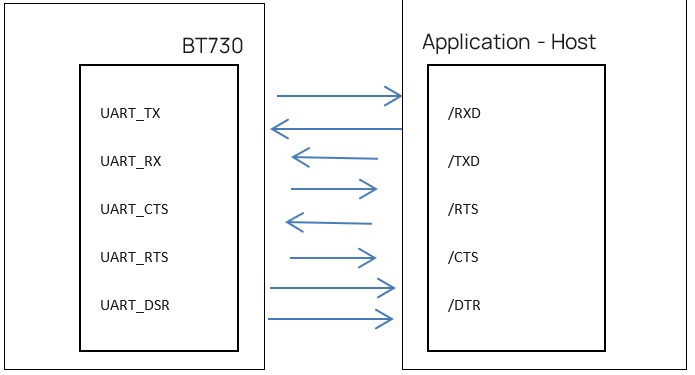
Note: The serial module output is at 3.3 V CMOS logic levels. Level conversion must be added to interface with an RS-232 level compliant interface.
Some serial implementations link CTS and RTS to remove the need for handshaking. Ezurio does not recommend linking CTS and RTS other than for testing and prototyping. If these pins are linked and the host sends data at the point that the BT730 deasserts its RTS signal, then there is a significant risk that internal receive buffers will overflow; this could lead to an internal processor crash. This also leads to a drop in connection and may require a power cycle to reset the module. Ezurio recommends that the correct CTS/RTS handshaking protocol be followed for proper operation.
SPI
The module is a slave device that uses terminals SPI_MOSI, SPI_MISO, SPI_CLK, and SPI_CSB. This interface is used for program firmware updates ONLY at the factory. Ezurio supplies a PC-based utility to allow a firmware upgrade over the UART port. It is highly recommended that customers use the UART method for updating firmware.
Note: The designer should be aware that no security protection is built into the hardware or firmware associated with this port, so the terminals should not be permanently connected in a PC application.
GPIO
Seven lines of programmable bi-directional input/outputs (I/O) are provided that can be accessed either via the UART port or Over-the-Air (OTA) from a second Bluetooth unit. These can be used as data inputs or to control external equipment. By using these in OTA mode, a BT730 module can be used for control and data acquisition without the need for any additional host processor. Each of the GPIO[3:9] ports can be independently configured to be either an input or output. A selection of ports can be accessed synchronously.
The ports are powered from internal VCC_3V3. The mode of these lines can be configured and the lines are accessed via S Registers 623 to 629.
ADC
The BT730 provides access to two 8-bit ADCs (Analogue 0 and 1). These provide an input range of 0 mV to 1,800 mV, which can be read using the S registers 701 and 702.
Suitable external scaling and over-voltage protection should be incorporated in your design. The module provides five samples per second at the UART with a baud rate of 115,200 or above.
nRESET Pin
Power-on-reset (power cycling and brown out consideration) — The reset circuitry within the BT730 module incorporates a brown-out detector; this may simplify power supply design. The BT730 reset line is an active low input (input debounced so must be low for more than 5 ms to cause a reset). Upon the application of power, the Power On Reset circuit built into the module ensures that the unit starts correctly. There is no need for an external power reset monitor.
RF
The BT730-SA on-board chip monopole antenna radiated performance depends on the host PCB layout. BT730 carrier board was used for BT730-SA development and antenna performance evaluation. To obtain similar performance, follow the guidelines in PCB Layout on Host PCB for BT730-SA to allow the on-board antenna to radiate and reduce proximity effects due to nearby host PCB GND copper or metal covers.
BT730-SA on-board antenna datasheet can be accessed from the following link:
http://www.acxc.com.tw/product/at3216/AT3216-B2R7HAA_071204.pdf
PCM Interface
PCM_OUT, PCM_IN, PCM_CLK, and PCM_SYNC carry up to three bi-directional channels of voice data, each at 8 k samples/s. The format of the PCM samples can be 8-bit A-law, 8-bit μ-law, 13-bit linear, or 16-bit linear. The PCM_CLK and PCM_SYNC terminals can be configured as inputs or outputs, depending on whether the module is the master or slave of the PCM interface. Please contact an Ezurio FAE for further details.
The module is compatible with the Motorola SSI™ interface and interfaces directly to PCM audio codec chips including the following:
- OKI 7702 single channel A-law and μ-law CODEC
- Winbond W681360 13 bit linear CODEC
Hardware Architecture
Block Diagrams
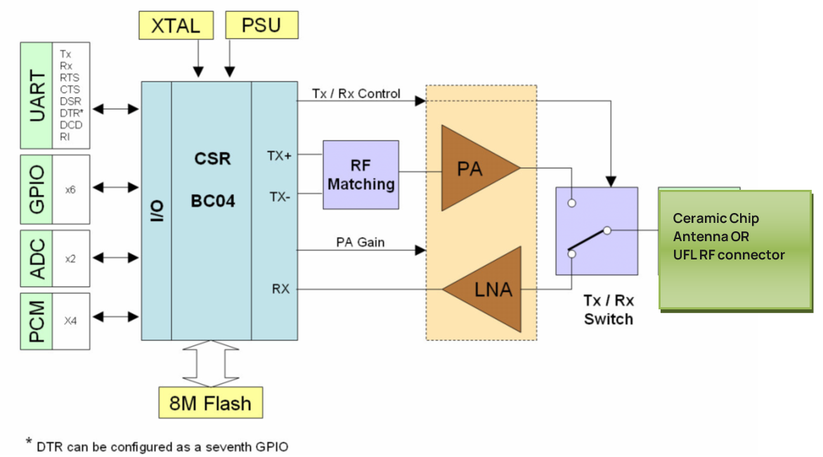
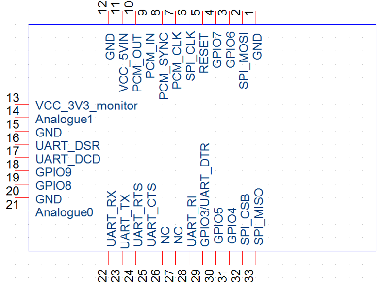
Pin-Out / Package Layout
Pin Definitions
| Pin | Signal | Description | Comment |
|---|---|---|---|
| 1 | GND | ||
| 2 | SPI_MOSI | SPI bus serial I/P | See Note 2 |
| 3 | GPIO6 | I/O for host | |
| 4 | GPIO7 | I/O for host | |
| 5 | nRESET | Module reset I/P | See Note 3 |
| 6 | SPI_CLK | SPI bus clock I/P | See Note 2 |
| 7 | PCM_CLK | PCM clock I/P | |
| 8 | PCM_SYNC | PCM sync I/P | |
| 9 | PCM_IN | PCM data I/P | |
| 10 | PCM_OUT | PCM Data O/P | |
| 11 | VCC_IN | 3.3 V < VCC_IN < 5.0 V | See Note 4 |
| 12 | GND | ||
| 13 | VCC_3V3_monitor | 3.3 V Monitor (do not connect) | See Note 5 |
| 14 | Analogue 1 | 1.8 V max | |
| 15 | GND | ||
| 16 | UART_DSR | UART_DSR I/P | |
| 17 | UART_DCD | UART_DCD I/P or O/P | |
| 18 | GPIO_9 | I/O for host | |
| 19 | GPIO_8 | I/O for host | |
| 20 | GND | ||
| 21 | Analogue 0 | 1.8 V max | |
| 22 | UART_RX | Receive data I/P | |
| 23 | UART_TX | Transmit data O/P | |
| 24 | UART_RTS | Request to Send O/P | |
| 25 | UART_CTS | Clear to Send I/P | |
| 26 | NC (Reserved USB_D+) | Not used for AT module variants | |
| 27 | NC (Reserved USB_D-) | Not used for AT module variants | |
| 28 | UART_RI | Ring Input or Output | |
| 29 | GPIO_3/UART_DTR | I/O for host/UART_DTR | |
| 30 | GPIO_5 | I/O for host | |
| 31 | GPIO_4 | I/O for host | |
| 32 | SPI_CSB | SPI bus chip select I/P | See Note 2 |
| 33 | SPI_MISO | SPI bus serial O/P | See Note 2 |
Notes:
- Unused pins may have internal connections and must not be connected.
- Pins 2, 6, 32, and 33 (SPI related) are only for Ezurio internal production purposes.
- Power-on-reset (power cycling and brown out consideration) — The reset circuitry within the BT730 module incorporates a brown-out detector; this may simplify power supply design. The BT730 reset line is an active low input (input debounced so must be low for more than 5 ms to cause a reset). Upon the application of power, the Power On Reset circuit built into the module ensures that the unit starts correctly. There is no need for an external power reset monitor.
- Power Supply Consideration — The power supply for the module should be a single voltage source of VCC within the VCC_IN range of 3.3 V to 5.0 V. It must be able to provide sufficient current in a transmit burst. This can rise to 200 mA. To limit dissipation, it is recommended that you use a voltage at the lower end of the range.
- The module includes regulators to provide internal local 3.3 V. This rail is accessible on pin 13 for monitoring purposes only. Under no circumstances should this pin be used to source current.
DSR, DTR, RI and DCD are configurable either as GPIO or as modem control lines.
Compatibility Note for Legacy Devices
If Reset compatibility is required with BTM402 and BTM404: Reset logic must be inverted (on the host PCB), by using suitable BJT (MMBT3904) with collector connected to Reset pin BT730 module pin 5. A fixed 10k Ohm pull down resistor to ground (BJT input) then ensures that the BT730 module is out of reset for the condition when host has yet to control the reset line.
Add a 10-k pull-up to the host PCB on the UART_RX, or the module remains in deep sleep if not driven to high.
Add a 10-k pull-down to the host PCB on the UART_CTS that if it is not connected (which we do not recommend) then the default state for UART_CTS input will be asserted which means can send data out of UART_TX line.
- GPIO lines can be configured through software to be either inputs or outputs with weak or strong pull-ups or pull-downs. At reset, all GPIO lines are configured as inputs with weak pull-downs.
- UART_RX, UART_TX, UART_CTS, UART_RTS, UART_RI, UART_DCD, and UART_DSR are 3.3 V level logic. For example, when RX and TX are idle they sit at 3.3 V. Conversely, for handshaking pins CTS, RTS, RI, DCD, and DSR, a 0 V is treated as an assertion.
- Pin 28 (UART_RI) is active low. It is normally 3.3 V. When a remote device initiates a connection, this pin goes low. When this pin is converted to RS232 voltage levels, it has the correct voltage level for assertion.
- Pin 17 (UART_DCD) is active low. It is normally 3.3 V. When a connection is live, this pin is low. This means that when this pin is converted to RS232 voltage levels it has the correct voltage level for assertion.
- Pin 16 (UART_DSR) is an input, with active low logic. It should be connected to the DTR output of the host. When the BTM730 module is in high speed mode (see S Register 507 in the Firmware User manual), this pin should be asserted by the host to ensure that the connection is maintained. A deassertion means that the connection should be dropped or an online command mode is being requested.
- Pin 13 (VCC_3V3 monitor) may only be used for monitoring (must not be used as a current source).
- The GPIO pins can be accessed using S Registers 623 to 629.
- GPIO3 is also used for DTR output (active low). See S Register 552 and 553 in the Firmware User manual.
- Analogue 0 and 1 should not exceed 1.8 V and S Registers 701 and 702 are used to access them.
Mechanical Drawings
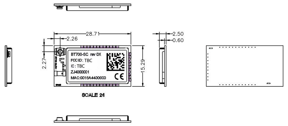
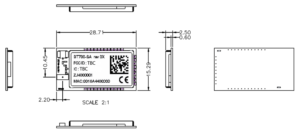
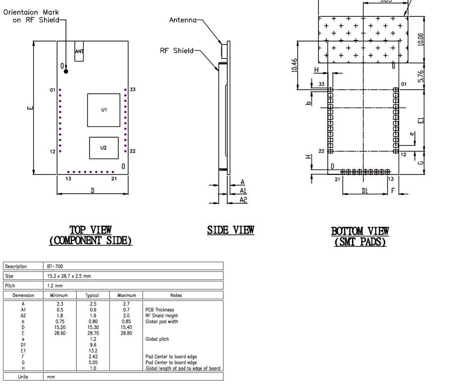
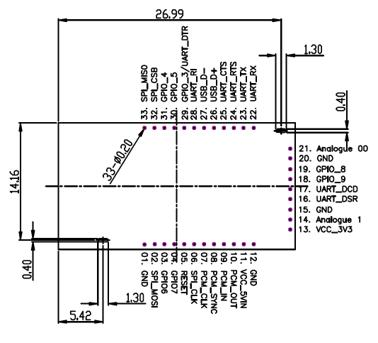
PCB Land Pattern and Antenna Keep-out for BT730-SA — Application Notes:
- Ensure there is no copper in the antenna 'keep out area' on any layers of the host PCB. Also keep all mounting hardware or any metal clear of the area to reduce effects of proximity detuning the antenna and to help antenna radiate properly. Refer to section Antenna Keep-Out on Host PCB for more information.
- For BT730-SA (with on-board chip antenna) best antenna performance, the module BT730-SA must be placed on the edge of the host PCB and preferably in the corner with the antenna facing the corner. The module is placed in the corner of host PCB above the keep-out area. If the BT730-SA is not placed in corner but on edge of host PCB, the antenna keep-out area must be modified.
- Ensure that there is no exposed copper under the module on the host PCB.
- The user may modify the PCB land pattern dimensions based on their experience and capability.
Host Interface Specifications
Electrical Characteristics
Absolute Maximum Ratings
Absolute maximum ratings for supply voltage and voltages on digital and analogue pins of the module are listed below; exceeding these values will cause permanent damage.
| Parameter | Min | Max | Unit |
|---|---|---|---|
| Peak current of power supply | 0 | 200 | mA |
| Voltage at digital pins | -0.4 | 3.7 | V |
| Voltage at POWER pin | 2.9 | 6.0 | V |
Recommended Operating Conditions
| Signal Name | Pin No | I/O | Voltage Level | Comments |
|---|---|---|---|---|
| VCC_IN | 11 | I | 3.3 V to 5.0 V * (Typ 3.5 V) | I typ = 115 mA |
| GND | 1, 12, 15, 20 | Four (4) ground terminals to be attached in parallel. | ||
| VCC_3V3_monitor | 13 | O | 3.3 V typical | For monitoring only. No current source. |
Note: VCC_3V3_monitor refers to internal voltage generated by the LDO inside the module which is typically 3.3 V. So to achieve 3.3 V for VCC_3V3_monitor (at Max Tx Power) requires VCC_IN of 3.5 V. IO voltage levels follow VCC_3V3_monitor. At minimum VCC_VIN of 3.3 V, the internal LDO generates 3.3 V but when Radio Tx at max Tx power, VCC_3V3_monitor drops a little (to ~3.15 V).
DC Electrical Characteristics
| Signal Type | Signal Level | Signal Level @ 0 mA load |
|---|---|---|
| Input | VILmin= -0.4 V; VILmax=0.8 V; VIHmin=2.3 V; VIHmax=3.7 V | |
| Output | VOLmax=0.2 V; VOHmin=3.1 V |
Signal Levels and Interface Specs
UART Interface
| Signal Name | Pin No | I/O | Comments |
|---|---|---|---|
| UART_TX | 23 | O | |
| UART_RX | 22 | I | |
| UART_CTS | 25 | I | |
| UART_RTS | 24 | O | |
| UART_DSR | 16 | I | |
| UART_DTR | 29 | O | Shared with GPIO3 |
| UART_RI | 28 | I or O | Direction may be programmed. |
| UART_DCD | 17 | I or O | Direction may be programmed. |
SPI Bus
| Signal Name | Pin No | I/O | Comments |
|---|---|---|---|
| SPI_MOSI | 2 | I | Ezurio INTERNAL USE ONLY — Used to reprogram Flash in Ezurio production. |
| SPI_MISO | 33 | O | |
| SPI_CSB | 32 | I | |
| SPI_CLK | 6 | I |
PCM Interface
| Signal Name | Pin No | I/O | Comments |
|---|---|---|---|
| PCM_CLK | 7 | I or O | If unused keep pins open. PCM output signals are tri-stated when there is not an active SCO or eSCO connection. |
| PCM_IN | 9 | I | |
| PCM_SYNC | 8 | I or O | |
| PCM_OUT | 10 | O |
General Purpose I/O and ADC
| Signal Name | Pin No | I/O | Signal Level | Comments |
|---|---|---|---|---|
| GPIO_3 – 9 | 3, 4, 16, 17, 18, 19, 29, 30, 31 | I or O | See Recommended Operating Conditions | |
| Analogue0, Analogue1 | 14, 21 | I | Range 0 – 1.8 V | 8 bit |
Miscellaneous
| Signal Name | Pin No | I/O | Signal Level | Comments |
|---|---|---|---|---|
| nRESET | 5 | I | VIL max=1.0V; VIH min=2.3V | Active LOW. The Reset input contains a 10 kΩ pull-up resistor (internal to module). |
Radio Characteristics
Bluetooth Receiver Characteristics
Receive Sensitivity: Better than -87 dBm (at 25°C)
Bluetooth Transmitter Characteristics
Max Transmit Power: 18 dBm into integrated antenna (BT730-SA); 16 dBm into UFL antenna connector (BT730-SC)
Min Transmit Power: -9 dBm into integrated antenna; -9 dBm into UFL antenna connector
Bluetooth Current Consumption
The current drain from the VCC power input line is dependent on various factors. The three most significant factors are the voltage level at VCC, UART baud rate, and the operating mode. The hardware specification for the module allows for a voltage range of 3.3 to 5.0 at VCC. The unit includes a linear regulator and tests have shown that there is no significant difference in current draw when VCC changes within the operating limits. Tests have shown that where power dissipation is an issue, it is best to keep VCC at the lower end of the range.
The UART baud rate has a bearing on power dissipation because, as is normal for digital electronics, the power requirements increase linearly with increasing clocking frequencies. Because of this, higher baud rates result in a higher current drain. Finally, the significant operating modes are: idle, waiting for a connection, inquiring, initiating a connection, sniff, and connected. With connected mode, it is also relevant to differentiate between no data being transferred and when data is being transferred at the maximum rate possible. The AT command set document describes how to configure the module for optimal power performance.
| Mode | Typical Average Current (mA) |
|---|---|
| Idle Mode, S512=1 | 1.25 mA |
| Wait for Connection or Discoverable Mode, AT+BTP S508=S510=640, S509=S511=320 | 55 mA |
| Wait for Connection or Discoverable Mode, AT+BTP S508=S510=1000, S509=S511=11 | 2.7 mA |
| Inquiry Mode, AT+BTI | 65 mA |
| Connecting Mode (ATDxxx) | 66 mA |
| Connected Mode (No Data Transfer) | 6 mA |
| Connected Mode (Max Data Transfer) | 35 mA |
| Sniff Mode S564=1000, S563=500, S562=50, S561=10 | 1.8 mA |
VCC_IN = 3.8 V, Baudrate = 9600 bps, Separation Distance = 15 meters
Power Management & Consumption
Power Consumption
See Bluetooth Current Consumption for typical current consumption values by operating mode.
Integration Guidelines
Antenna Characteristics
The BT730-SA on-board chip monopole antenna radiated performance depends on the host PCB layout. BT730 carrier board was used for BT730-SA development and antenna performance evaluation. To obtain similar performance, follow the guidelines in PCB Layout on Host PCB for BT730-SA.
BT730-SA on-board antenna datasheet: http://www.acxc.com.tw/product/at3216/AT3216-B2R7HAA_071204.pdf
Circuit (Overview and Checklist)
The BT730 series module is easy to integrate requiring no external components on the customer's board apart from those required by customer for development and in customer's end application.
Checklist (for the schematic):
- VCC_IN: External power source within the operating range specification of BT730-Sx. Add decoupling (or bulk) capacitors for filtering (or reservoir) the external source. Power-on reset circuitry within BT730-Sx series module incorporates brown-out detector, thus simplifying power supply design. Upon application of power, the internal power-on reset ensures module starts correctly.
- AIN (ADC) and GPIO (or UART) pin IO voltage levels: BT73-Sx GPIO voltage levels are at VCC_3V3_monitor pin (see section Recommended Operating Conditions). Ensure input voltage levels into GPIO pins are at VCC_3V3_monitor voltage levels. Ensure ADC pin maximum input voltage (1.8 V) for damage is not violated.
- UART: Is required. Add connector to allow UART to be interfaced to PC (via UART–RS232 or UART–USB).
- UART_RX and UART_CTS: Add a 10 k pull-up to the host PCB on the UART_RX, otherwise the module remains in deep sleep if not driven to high. The pull-up prevents the module from going into deep sleep when UART_RX line is idling. Add a 10 k pull-down to the host PCB on the UART_CTS that, if it is not connected (which we do not recommend) then the default state for UART_CTS input will be asserted which means can send data out of UART_TX line.
- nRESET pin (active low): Hardware reset. Wire out to push button or drive by host. If used external reset must be exerted for a minimum of 5 mS. By default, the module is out of reset when power is applied to the VCC pin.
- PCM: All four PCM signals are routed directly from chipset to external BT730-Sx module pins. It is then up to customer to configure appropriately. A 4.7 k pull down resistor to ground on PCM_OUT may help resolve audio noise problems when chipset PCM_OUT line tristates.
PCB Layout
PCB Layout on Host PCB - General
Checklist (for PCB):
- MUST locate the BT730-SA module close to the edge of PCB (mandatory for BT730-SA for on-board chips antenna to radiate properly).
- Use solid GND plane on inner layer (for best EMC and RF performance).
- Place GND vias as close to module GND pads as possible.
- Unused host PCB area on surface layer can be flooded with copper but place GND vias regularly to connect copper flood to inner GND plane. If GND flood copper underside the module then connect with GND vias to inner GND plane.
- Route traces to avoid noise being picked up on VCC_IN supply, Analogue and GPIO (digital) traces.
- Ensure there is no exposed copper on the underside of the module (refer to land pattern drawing of BT730-Sx).
Antenna Keep-Out on Host PCB
The BT730-SA has an integrated chip antenna and its performance is sensitive to the host PCB. It is critical to locate the BT730-SA on the edge of the host PCB (or corner) for proper radiation. Refer to guidelines in the section PCB Land Pattern and Antenna Keep-out area for BT730-SA. Some guidelines are repeated below.
- Ensure there is no copper in the antenna keep-out area on any layers of the host PCB. Keep all mounting hardware and metal clear of the area to allow proper antenna radiation.
- For best antenna performance, place the BT730-SA module on the edge of the host PCB, preferably in the corner with the antenna facing the corner. An example shown in Figure 3.
- A different host PCB thickness dielectric will have small effect on antenna (the BT730 carrier development board (used for antenna performance evaluation) thickness was 0.78 mm).
- The antenna-keep-out defined in PCB Land Pattern and Antenna Keep-out area for BT730-SA applies when the BT730-SA is placed in the corner of the host PCB. When BT730-SA cannot be placed as such, it must be placed on the edge of the host PCB and a modified antenna keep out must be observed. This antenna keep-out modification is shown in Figure 4 (antenna keep-out is extended by 8 mm on both sides).
Antenna Keep-out and Proximity to Metal or Plastic:
Figure 5 and Figure 6 show the recommended and not recommended locations for metal with respect to a BT730-SA module on-board antenna.
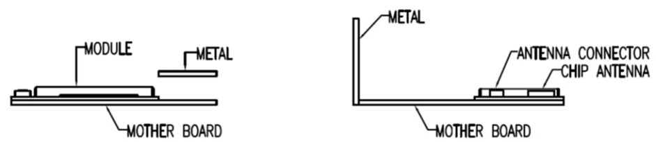

- Minimum safe distance for metals without seriously compromising the antenna (tuning) is 40 mm top/bottom and 30 mm left or right.
- Metal close to the BT730-SA chip monopole antenna (bottom, top, left, right, any direction) will have degradation on the antenna performance. The amount of degradation is entirely system dependent which means some testing by customer is required (in their host application).
- Anything metal closer than 20 mm starts to significantly degrade performance (S11, gain, radiation efficiency).
- It is best that the customer tests the range with a mock-up (or actual prototype) of the product to assess effects of enclosure height (and material, whether metal or plastic).
PCB Layout on Host PCB for BT730-SA
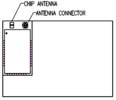
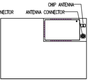
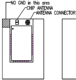
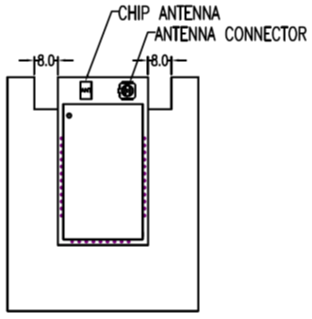
Note: Copper cut-away on all layers in "antenna keep-out" area under BT730-SA module on host PCB. Refer to "antenna keep-out" defined in section 7.4 PCB Land Pattern and Antenna Keep-out for BT730-SA.
External Antenna Integration
Refer to the regulatory sections for FCC, ISED, and the EU for details of use of BT730-SC with external antennas in each regulatory region.
The BT730-SC family has been designed to operate with the antennas listed below with a maximum gain of 2 dBi. The required antenna impedance is 50 ohms. External antennas improve radiation efficiency.
| Item | Part Number | Mfg. | Type | Gain (dBi) | Connector Type |
|---|---|---|---|---|---|
| 1 | MAF94045 | Ezurio (Laird Connectivity) | Internal | 2 | UFL |
| 2 | WRR2400-IP04-B (MAF94019) | Ezurio (Laird Connectivity) | Dipole | 1.5 | UFL |
| 3 | WTC2450-IP04-K (MAF94006) | Ezurio (Laird Connectivity) | Dipole | 2 | UFL |
| 4 | S181FL-L-RMM-2450S | Nearson (Laird) | Dipole | 2 | UFL |
Note 1: Integral RF co-axial cable with UFL connector.
Antenna manufacturer Ezurio contact information:
Email: support@ezurio.com
Application Note for Surface Mount Modules
Introduction
Ezurio surface mount modules are designed to conform to all major manufacturing guidelines. This application note is intended to provide additional guidance beyond the information that is presented in the user manual. This application note is considered a living document and will be updated as new information is presented.
The modules are designed to meet the needs of a number of commercial and industrial applications. The modules are designed to be easily manufactured and conform to current automated manufacturing processes.
Note: Units are in mm.
Reflow Parameters
Ezurio surface mount modules are designed to be easily manufactured including reflow soldering to a PCB. It is ultimately the responsibility of the customer to choose the appropriate solder paste and to ensure oven temperatures during reflow meet the requirements of the solder paste. Ezurio's surface mount modules conform to J-STD-020D1 standards for reflow temperatures.
Important: During reflow, modules should not be above 260° and not for more than 30 seconds.
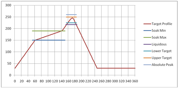
Temperatures should not exceed the minimums or maximums presented in the following table.
| Specification | Value | Unit |
|---|---|---|
| Temperature Inc./Dec. Rate (max) | 1~3 | °C / Sec |
| Temperature Decrease rate (goal) | 2-4 | °C / Sec |
| Soak Temp Increase rate (goal) | 0.5 – 1 | °C / Sec |
| Flux Soak Period (Min) | 70 | Sec |
| Flux Soak Period (Max) | 120 | Sec |
| Flux Soak Temp (Min) | 150 | °C |
| Flux Soak Temp (max) | 190 | °C |
| Time Above Liquidous (max) | 70 | Sec |
| Time Above Liquidous (min) | 50 | Sec |
| Time In Target Reflow Range (goal) | 30 | Sec |
| Time At Absolute Peak (max) | 5 | Sec |
| Liquidous Temperature (SAC305) | 218 | °C |
| Lower Target Reflow Temperature | 240 | °C |
| Upper Target Reflow Temperature | 250 | °C |
| Absolute Peak Temperature | 260 | °C |
Shipping and Labeling
Packaging
Modules are shipped in ESD (Electrostatic Discharge) safe trays that can be loaded into most manufacturers pick and place machines. Layouts of the trays are provided in Figure 11.
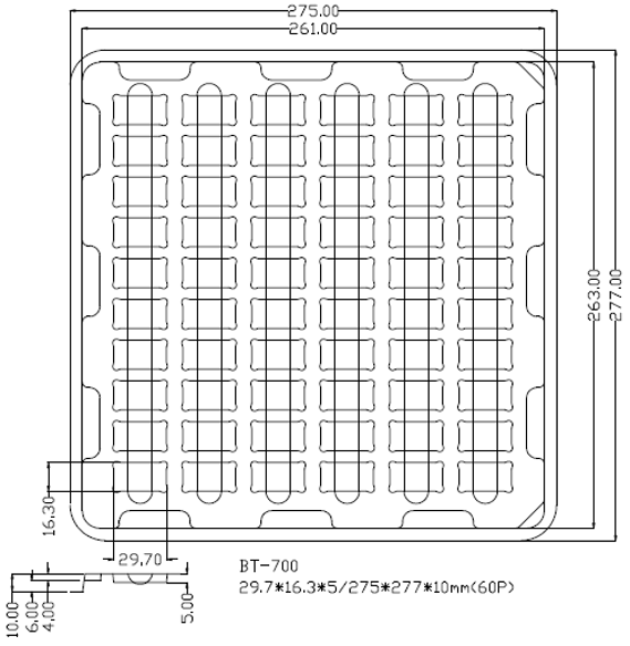
Regulatory, Qualification & Certifications
Regulatory Approvals
Note: For complete regulatory information, refer to the BT730 Regulatory Information document which is also available from the BT730 product page.
The BT730-SA/BT730-SC holds current certifications in the following countries:
| Country/Region | Regulatory ID |
|---|---|
| USA (FCC) | SQGBT700 |
| EU | N/A |
| Canada (ISED) | 3147A-BT700 |
Bluetooth SIG Qualification
The Bluetooth Qualification Process promotes global product interoperability and reinforces the strength of the Bluetooth® brand and ecosystem to the benefit of all Bluetooth SIG members. The Bluetooth Qualification Process helps member companies ensure their products that incorporate Bluetooth technology comply with the Bluetooth Patent & Copyright License Agreement and the Bluetooth Trademark License Agreement (collectively, the Bluetooth License Agreement) and Bluetooth Specifications.
The Bluetooth Qualification Process is defined by the Qualification Program Reference Document (QPRD) v3.
To demonstrate that a product complies with the Bluetooth Specification(s), each member must for each of its products:
- Identify the product, the design included in the product, the Bluetooth Specifications that the design implements, and the features of each implemented specification
- Complete the Bluetooth Qualification Process by submitting the required documentation for the product under a user account belonging to your company
The Bluetooth Qualification Process consists of the phases shown below:
To complete the Qualification Process the company developing a Bluetooth End Product shall be a member of the Bluetooth SIG. To start the application please use the following link: Apply for Adopter Membership
Scope
This guide is intended to provide guidance on the Bluetooth Qualification Process for End Products that reference a single existing design, that has not been modified (refer to Section 3.2.1 of the Qualification Program Reference Document v3).
This option applies to a Member qualifying a Product that includes an existing Design that has a DN, QDID, or DID and that Design has not been modified (e.g., rebranding a Qualified Product from another Member). The Design identified by the DN, QDID, or DID may only implement Bluetooth Specifications that are active or deprecated at the time of Submission. No modifications may be made to the Design, including changes to the ICS Form.
Changes to the Product outside the Design are allowed, including:
- Enabling technologies
- Changes to the industrial design
- Changes to the communication technology other than Bluetooth
- Changes to the features that are unrelated to Bluetooth, branding, packaging, colour, shape, Product name, or Model number
Members are responsible for assessing that modifications to the Product outside of the Design do not affect compliance with Bluetooth Specifications or result in a change to the ICS Form.
For the purposes of this document, it is assumed that the member is combining a single unmodified Core-Complete Configuration.
Qualification Steps
For this qualification, follow these steps:
- To start a listing, go to: https://qualification.bluetooth.com/
- Select Start the Bluetooth Qualification Process.
Product Details to be entered:
- Project Name (this can be the product name or the Bluetooth Design name).
- Product Description
- Model Number
- Product Publication Date (the product publication date may not be later than 90 days after submission)
- Product Website (optional)
- Internal Visibility (this will define if the product will be visible to other users prior to publication)
- If you have multiple End Products to list then you can select 'Import Multiple Products', firstly downloading and completing the template, then by 'Upload Product List'. This will populate Qualification Workspace with all your products.
Specify the Design:
- Do you include any existing Design(s) in your Product? Answer Yes, I do.
- Enter the single DN or QDID used in your, (for Option 1 only one DN or QDID can be referenced)
- Once the DN or QDID is selected it will appear on the left-hand side, indicating the layers covered by the design.
- Select 'I'm finished entering DN's
- What do you want to do next? Answer, 'Use this Design without Modification'
- Save and go to Product Qualification Fee
Product Qualification Fee:
- It's important to make sure a Prepaid Product Qualification fee is available as it is required at this stage to complete the Qualification Process.
- Prepaid Product Qualification Fee's will appear in the available list so select one for the listing.
- If one is not available select 'Pay Product Qualification Fee', payment can be done immediately via credit card, or you can pay via Invoice. Payment via credit will release the number immediately, if paying via invoice the number will not be released until the invoice is paid.
- Once you have selected the Prepaid Qualification Fee, select 'Save and go to Submission'
Submission:
- Some automatic checks occur to ensure all submission requirements are complete.
- To complete the listing any errors must be corrected
- Once you have confirmed all design information is correct, tick all of the three check boxes and add your name to the signature page.
- Now select 'Complete the Submission'.
- You will be asked a final time to confirm you want to proceed with the submission, select 'Complete the Submission'.
- Qualification Workspace will confirm the submission has been submitted. The Bluetooth SIG will email confirmation once the submission has been accepted, (normally this takes 1 working day).
Download Product and Design Details:
- You can now download a copy of the confirmed listing from the design listing page and save a copy in your Compliance Folder
For further information: https://www.bluetooth.com/develop-with-bluetooth/qualification-listing/
Example Designs for Reference
| Design Name | Owner | Declaration ID | QD ID | Link |
|---|---|---|---|---|
| BT7x0 Series | Ezurio | D049591 | 147394 | https://qualification.bluetooth.com/ListingDetails/104900 |
Qualify More Products
If you develop further products based on the same design in the future, it is possible to add them free of charge. The new product must not modify the existing design (i.e. add ICS functionality), otherwise a new design listing will be required.
To add more products to your design, select 'Manage Submitted Products' in the Getting Started page, Actions, Qualify More Products. The tool will take you through the updating process.
Ordering Information
| Part Number | Description |
|---|---|
| BT730-SA | Class 1 Bluetooth V2.0 Module (internal antenna) |
| BT730-SC | Class 1 Bluetooth v2.0 Module (uFL for external antenna) |
| DVK–BT730-SA | Development board with BT730-SA module soldered in place |
| DVK–BT730-SC | Development board with BT730-SC module soldered in place |
Additional Support & Appendices
Please contact your local sales representative or our support team for further assistance:
| Headquarters | Ezurio 50 S. Main St. Suite 1100 Akron, OH 44308 USA |
| Website | http://www.ezurio.com |
| Technical Support | http://www.ezurio.com/resources/support |
| Sales Contact | http://www.ezurio.com/contact |
Note: Information contained in this document is subject to change. Ezurio's products are subject to standard Terms & Conditions. © Copyright 2026 Ezurio All Rights Reserved. Any information furnished by Ezurio and its agents is believed to be accurate but cannot be guaranteed. All specifications are subject to change without notice. Responsibility for the use and application of Ezurio materials or products rests with the end user since Ezurio and its agents cannot be aware of all potential uses. Ezurio makes no warranties as to non-infringement nor as to the fitness, merchantability, or sustainability of any Ezurio materials or products for any specific or general uses. Ezurio or any of its affiliates or agents shall not be liable for incidental or consequential damages of any kind. All Ezurio products are sold pursuant to the Ezurio Terms and Conditions of Sale in effect from time to time, a copy of which will be furnished upon request. Nothing herein provides a license under any Ezurio or any third-party intellectual property right. Ezurio and its associated logos are trademarks owned by Ezurio and/or its affiliates.
| Ver. | Date | Notes | Contributor | Approver |
|---|---|---|---|---|
| 1.0 | 19 June 2013 | Initial Release | Jonathan Kaye | |
| 1.1 | 23 June 2013 | Replaced "PCB Land Pattern and Antenna Keep-out for BT730-SA" image; fixed incorrect text; updated table captions | Jonathan Kaye | |
| 1.2 | 30 August 2013 | Removal of OBEX Client; Updated Bluetooth SIG Approvals | Jonathan Kaye | |
| 1.3 | 30 Sept 2013 | Updated BT730-SA placement on host PCB image | Jonathan Kaye | |
| 1.4 | 06 Feb 2014 | Updated Bluetooth SIG Qualification section | Jonathan Kaye | |
| 1.5 | 15 Aug 2016 | Changed from Hardware Integration Guide to Datasheet | Sue White | |
| 1.6 | 19 Sept 2016 | Updated EU Declaration of Conformity | Sue White | |
| 1.7 | 16 June 2017 | Updated EU Doc with new RED standards | Tom Smith | |
| 1.8 | 25 Aug 2020 | Updated mechanical drawing | Jonathan Kaye | |
| 1.9 | 20 Nov 2020 | Updated all regulatory information | Ryan Urness | Jonathan Kaye |
| 2.0 | 28 Jan 2021 | Moved all regulatory information into a separate document | Sue White | Jonathan Kaye |
| 2.1 | 6 Nov 2024 | Updates to Bluetooth SIG Qualification | Dave Drogowski | Jonathan Kaye |
| 3.0 | 24 Jan 2024 | Updated to Ezurio branding | Dave Drogowski | Dave Drogowski |
| 3.1 | 14 Apr 2025 | Updated MSL level to MSL 4 | Dave Drogowski | Jonathan Kaye |