/filters:background_color(white)/2024-03/LWB5-Plus-Modules-And-USB1.png)
Scope
This document describes key hardware aspects of the Ezurio Sterling™ LWB5+ series wireless modules providing either SDIO or USB2.0 interface for WLAN connection and UART/PCM, USB2.0/PCM for Bluetooth® connection. This document is intended to assist device manufacturers and related parties with the integration of this radio into their host devices. Data in this document is drawn from several sources and includes information found in the Cypress CYW4373EUBGT data sheet issued in July 2020 along with other documents provided from Cypress.
Note: The information in this document is subject to change. Please contact Ezurio to obtain the most recent version of this document.
Introduction
Overview
This document describes key hardware aspects of the Sterling-LWB5+. This document is intended to assist device manufacturers and related parties with the integration of this radio into their host devices. Data in this document is drawn from several sources. For full documentation on the Sterling-LWB5+, visit:
General Description
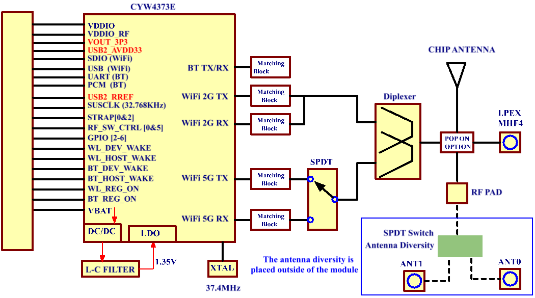
The LWB5+ series wireless module is an integrated, small form factor 1x1 SISO 802.11 a/b/g/n/ac WLAN plus dual-mode Bluetooth® 5.2 Low Energy module that is optimized for low-power mobile devices. The integration of all WLAN and Bluetooth functionality in a single package supports low cost and simple implementation along with flexibility for platform-specific customization.
This device is pre-calibrated and integrates the complete transmit/receive RF paths including diplexer, switches, reference crystal oscillator, and power management units (PMU). The integrated ceramic chip antenna, MHF4 RF connector, and RF trace pad are selectable from different variants.
The LWB5+ series device supports IEEE 802.11ac 1x1 SISO with data rates up to MCS9 (433.3 Mbps). An internal Wi-Fi and Bluetooth coexistence scheme provides optimized connectivity while Wi-Fi and Bluetooth are working simultaneously. The device’s low power consumption radio architecture and power management unit (PMU) proprietary power save technologies allow for extended battery life.
In addition, its dual 802.11ac and Bluetooth radio includes full digital MAC and baseband engines that handle all 802.11 CCK/OFDM® 2.4/5 GHz and Bluetooth 5.2 (Basic Rate, Enhanced Data Rate, and Bluetooth Low Energy) baseband and protocol processing.
The LWB5+ series wireless modules include three product SKUs which have different RF path and antenna types. Please contact Ezurio Sales/FAE for further information.
This datasheet is subject to change. Please contact Ezurio for further information.
Features & Benefits
The Sterling-LWB5+ device features and benefits are described in the following table.
| Feature | Description | ||||||||||||||||
|---|---|---|---|---|---|---|---|---|---|---|---|---|---|---|---|---|---|
| Radio Front End |
| ||||||||||||||||
| Power Management | One buck regulator, multiple LDO regulators, and a power management unit (PMU) are integrated into the CYW4373E. All regulators are programmable via the PMU. These blocks simplify power supply design for Bluetooth and WLAN functions in embedded designs. | ||||||||||||||||
| Pre-Calibration | RF system tested and calibrated in production | ||||||||||||||||
| Sleep Clock | An external sleep clock of 32.768 kHz is required. | ||||||||||||||||
| Host Interface | SDIO v3.0 interface that can operate in 4b or 1b mode and a USB 2.0 interface. The Bluetooth section supports USB 2.0, USB 1.1, SDIO, and a high-speed 4-wire UART interface. An on-chip USB 2.0 hub provides a shared single USB connection to both WLAN and Bluetooth target devices.
| ||||||||||||||||
| Advanced WLAN |
| ||||||||||||||||
| Advanced Bluetooth |
|
Specification Summary
Processor / SoC / Chipset
| Wireless | Cypress CYW4373EUBGT |
Wi-Fi
| Standards | IEEE 802.11a, 802.11b, 802.11e, 802.11g, 802.11h, 802.11i, 802.11k*, 802.11n, 802.11r, 802.11v*, 802.11ac |
| Interface | 1-bit or 4-bit Secure Digital I/O; USB 2.0 |
| Spatial Streams | 1 (1x1 SISO) [802.11ac/n] |
| Channel Support | 2.4 GHz:
5 GHz:
|
| Supported Data Rates | Support 802.11 ac/a/b/g/n 1x1 SISO. 802.11b (DSSS, CCK) 1, 2, 5.5, 11 Mbps 802.11a/g (OFDM) 6, 9, 12, 18, 24, 36, 48, 54 Mbps 802.11n (OFDM, HT20/HT40, MCS0-7) 802.11ac (OFDM, VHT20, MCS0-8; OFDM, VHT40/HT80, MCS0-9) |
| Transmit Power Note: Transmit power on each channel varies per individual country regulations. All values are nominal with +/-2 dBm tolerance at room temperature. Tolerance could be up to +/-2.5 dBm across operating temperature. Note: HT40 – 40 MHz-wide channels | 802.11a
802.11b
802.11g
802.11n (2.4 GHz)
802.11n (5 GHz)
802.11ac (5 GHz)
Bluetooth
Note: The EIRP of Bluetooth transmissions may not exceed 10 dBm. This includes the radio output power and the antenna gain used in combination with the radio. |
Typical Receiver Sensitivity (PER <= 10%) Note: All values nominal, +/-3 dBm. | 802.11a:
802.11b:
802.11g:
802.11n (2.4 GHz):
802.11n (5 GHz):
802.11ac (5 GHz):
Bluetooth:
|
| Modulation Schemes | BPSK, QPSK, CCK, 16-QAM, 64-QAM, and 256-QAM. 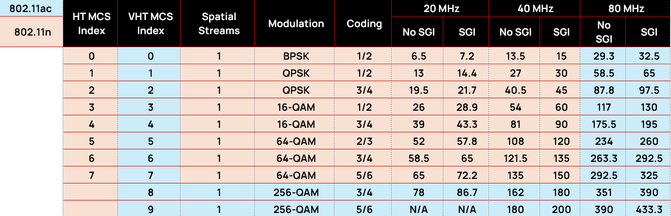 |
| Network Architecture Type | Infrastructure (client operation) |
| Wi-Fi Media | Direct Sequence-Spread Spectrum (DSSS) Complementary Code Keying (CCK) Orthogonal Frequency Divisional Multiplexing (OFDM) |
| Wi-Fi Multimedia | WMM Wi-Fi Multimedia - PowerSave (WMM-PS with U-APSD) WMM-Sequential Access (WMM-SA with PCF) |
Bluetooth
| Standards | Bluetooth 5.2 Core Spec |
| Interface | Host Controller Interface (HCI) using high speed UART, USB 2.0 |
| Supported Data Rates | 1, 2, 3 Mbps |
| Bluetooth LE Modulation | GFSK@ 1 Mbps Pi/4-DQPSK@ 2 Mbps 8-DPSK@ 3 Mbps |
| Bluetooth Media | Frequency Hopping Spread Spectrum (FHSS) |
Radio Performance
| 2.4 GHz Frequency Bands | EU: 2.4 GHz to 2.483 GHz FCC/ISED: 2.4 GHz to 2.473 GHz MIC: 2.4 GHz to 2.495 GHz RCM: 2.4 GHz to 2.483 GHz |
| 5 GHz Frequency Bands | EU 5.15 GHz to 5.35 GHz (Ch 36/40/44/48/52/56/60/64) 5.47 GHz to 5.725 GHz (Ch 100/104/108/112/116/120/124/128/132/136/140) 5.725 GHz to 5.85 GHz (Ch 149/153/157/161/165) FCC 5.15 GHz to 5.35 GHz (Ch 36/40/44/48/52/56/60/64) 5.47 GHz to 5.725 GHz (Ch 100/104/108/112/116/120/124/128/132/136/140/144 5.725 GHz to 5.85 GHz (Ch 149/153/157/161/165) ISED 5.15 GHz to 5.35 GHz (Ch 36/40/44/48/52/56/60/64) 5.47 GHz to 5.725 GHz (Ch 100/104/108/112/116/132/136/140/144 5.725 GHz to 5.85 GHz (Ch 149/153/157/161/165) MIC 5.15 GHz to 5.35 GHz (Ch 36/40/44/48/52/56/60/64) 5.47 GHz to 5.725 GHz (Ch 100/104/108/112/116/120/124/128/132/136/140) RCM 5.15 GHz to 5.35 GHz (Ch 36/40/44/48/52/56/60/64) 5.47 GHz to 5.725 GHz (Ch 100/104/108/112/116/132/136/140 5.725 GHz to 5.85 GHz (Ch 149/153/157/161/165) |
| 6 GHz Frequency Bands | Complete / remove as needed |
Interfaces
| Physical Interfaces | 68-pin LGA package (including 17 thermal ground pads under the package) |
| Network Interfaces | Wi-Fi: 1-bit or 4-bit Secure Digital I/O; USB 2.0 Bluetooth: Host Controller Interface (HCI) using high speed UART, USB 2.0 |
Power
| Input Voltage | Operational: VBAT is 3.2V to 4.8V ** EVM/harmonics are improved with VBAT ≥ 3.6V |
| I/O Signal Voltage | Typical DC 3.2V to 3.6V or DC 1.8 V ± 10% |
Mechanical
| Dimensions | Length: 17 (0.67) Width: 12 (0.47) Thickness: 2.13 (0.08) |
| Weight | ~0.7 (~0.02) |
Software
| OS Support | Linux Android |
| Security |
|
Environmental
| Operating Temperature | -40° to +85°C (-40° to +185°F) |
| Storage Temperature | -40° to +85°C (-40° to +185°F) |
| Operating Humidity | 10 to 90% (non-condensing) |
| Storage Humidity | 10 to 90% (non-condensing) |
| MSL (Moisture Sensitivity Level) | 4 |
| Maximum Electrostatic Discharge | Conductive 4KV; Air coupled 8KV (follow EN61000-4-2) |
| Lead Free | Lead-free and RoHS Compliant |
Certifications
| Regulatory Compliance | United States (FCC) EU - Member countries of European Union (ETSI) ISED (Canada) Australia Japan |
| Compliance Standards | EU
FCC
ISED Canada
MIC
|
| Bluetooth SIG | Bluetooth® SIG Qualification |
Development
| Development Kit | 453-00045-K1 Development Kit (Chip Antenna) 453-00046-K1 Development Kit (External Antenna) |
Warranty
| Warranty Terms | One Year Warranty |
Functional Descriptions
WLAN Functional Description
The LWB5+ series wireless module is designed based on the Cypress CYW4373EUBGT 802.11ac/a/b/g/n chipset. It is optimized for high speed, reliability, and low-power embedded applications. It is integrated with dual-band WLAN (2.4/5 GHz) and Bluetooth 5.2. Its functionality includes the following:
- Improved throughput on the link due to frame aggregation, RIFS (reduced inter-frame spacing), and half guard intervals.
- Support for LDPC (Low Density Parity Check) codes.
- Improved 11n performance due to features such as 11n frame aggregation (TX A-MPDU) and low-overhead host-assisted buffering (RX A-MPDU). These techniques can improve performance and efficiency of applications involving large bulk data transfers such as file transfers or high-resolution video streaming.
- IEEE 802.11ac, 1x1 SISO with data rate up to MCS9 (433.3 Mbps).
| Feature | Description | ||||||||||||||||||||||||||||||||||||||||||||||||||||||||||||||||||||||||||||||||||||||||||||||||||||||||||||||||||||||||||||||||||||||||||||||||||||||||||||||||||||||||||||||||||||||||||||||||||||||||||||||||||||||||
|---|---|---|---|---|---|---|---|---|---|---|---|---|---|---|---|---|---|---|---|---|---|---|---|---|---|---|---|---|---|---|---|---|---|---|---|---|---|---|---|---|---|---|---|---|---|---|---|---|---|---|---|---|---|---|---|---|---|---|---|---|---|---|---|---|---|---|---|---|---|---|---|---|---|---|---|---|---|---|---|---|---|---|---|---|---|---|---|---|---|---|---|---|---|---|---|---|---|---|---|---|---|---|---|---|---|---|---|---|---|---|---|---|---|---|---|---|---|---|---|---|---|---|---|---|---|---|---|---|---|---|---|---|---|---|---|---|---|---|---|---|---|---|---|---|---|---|---|---|---|---|---|---|---|---|---|---|---|---|---|---|---|---|---|---|---|---|---|---|---|---|---|---|---|---|---|---|---|---|---|---|---|---|---|---|---|---|---|---|---|---|---|---|---|---|---|---|---|---|---|---|---|---|---|---|---|---|---|---|---|---|---|---|---|---|---|---|---|
| WLAN MAC |
| ||||||||||||||||||||||||||||||||||||||||||||||||||||||||||||||||||||||||||||||||||||||||||||||||||||||||||||||||||||||||||||||||||||||||||||||||||||||||||||||||||||||||||||||||||||||||||||||||||||||||||||||||||||||||
| WLAN Security |
| ||||||||||||||||||||||||||||||||||||||||||||||||||||||||||||||||||||||||||||||||||||||||||||||||||||||||||||||||||||||||||||||||||||||||||||||||||||||||||||||||||||||||||||||||||||||||||||||||||||||||||||||||||||||||
| WLAN Channel | Channel frequency supported.
| ||||||||||||||||||||||||||||||||||||||||||||||||||||||||||||||||||||||||||||||||||||||||||||||||||||||||||||||||||||||||||||||||||||||||||||||||||||||||||||||||||||||||||||||||||||||||||||||||||||||||||||||||||||||||
Bluetooth Functional Description
The LWB5+ series wireless module includes a fully integrated Bluetooth baseband/radio.
| Feature | Description |
|---|---|
| Bluetooth Interface | Voice interface:
High-Speed UART interface USB 2.0 |
| Bluetooth Core functionality |
|
| Bluetooth Low Energy (BLE) Core functionality |
|
Crystal Oscillator Requirement
| 32.768 KHz Oscillator | |
|---|---|
| Frequency Accuracy | 200 ppm |
| Duty Cycle | 30% – 70% |
| Input Signal Amplitude | 200-3300 mV, peak-peak |
| Signal Type | Square or Sine Wave |
| Clock Jitter | <10,000 ppm |
IMPORTANT: A 32.768 KHz crystal is required for the module to be functional. The module will not boot without this crystal.
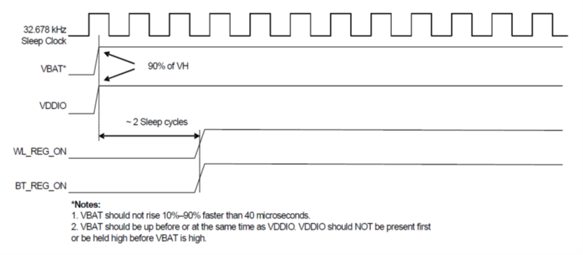
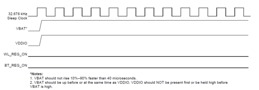
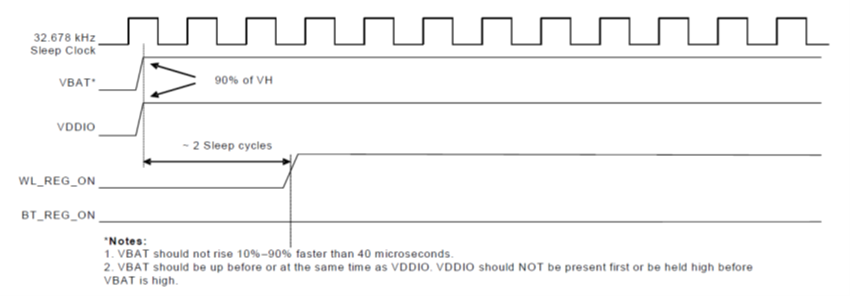
Power-Up Sequence and Timing
Boot Mode
Description of Control Signals
- WL_REG_ON – Used by the PMU to power-up the WLAN section. When this pin is high, the regulators are enabled and the WLAN section is out of reset. When this pin is low the WLAN section is in reset. If both the BT_REG_ON and WL_REG_ON pins are low, the regulators are disabled.
- BT_REG_ON – Used by the PMU (OR-gated with WL_REG_ON) to power-up the internal regulators. If both the BT_REG_ON and WL_REG_ON pins are low, the regulators are disabled. When this pin is low and WL_REG_ON is high, the BT section is in reset.
Notes:
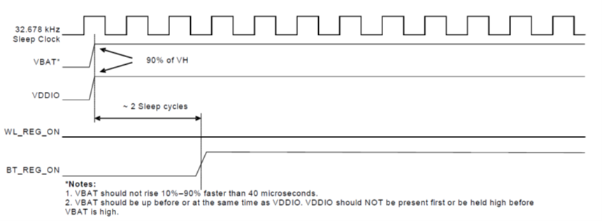
For both the WL_REG_ON and BT_REG_ON pins, there should be at least a 10-millisecond time delay between consecutive toggles (where both signals have been driven low). This allows time for the internal regulator to discharge. If this delay is not followed, there may be a VDDIO in-rush current on the order of 36 mA during the next PMU cold start.
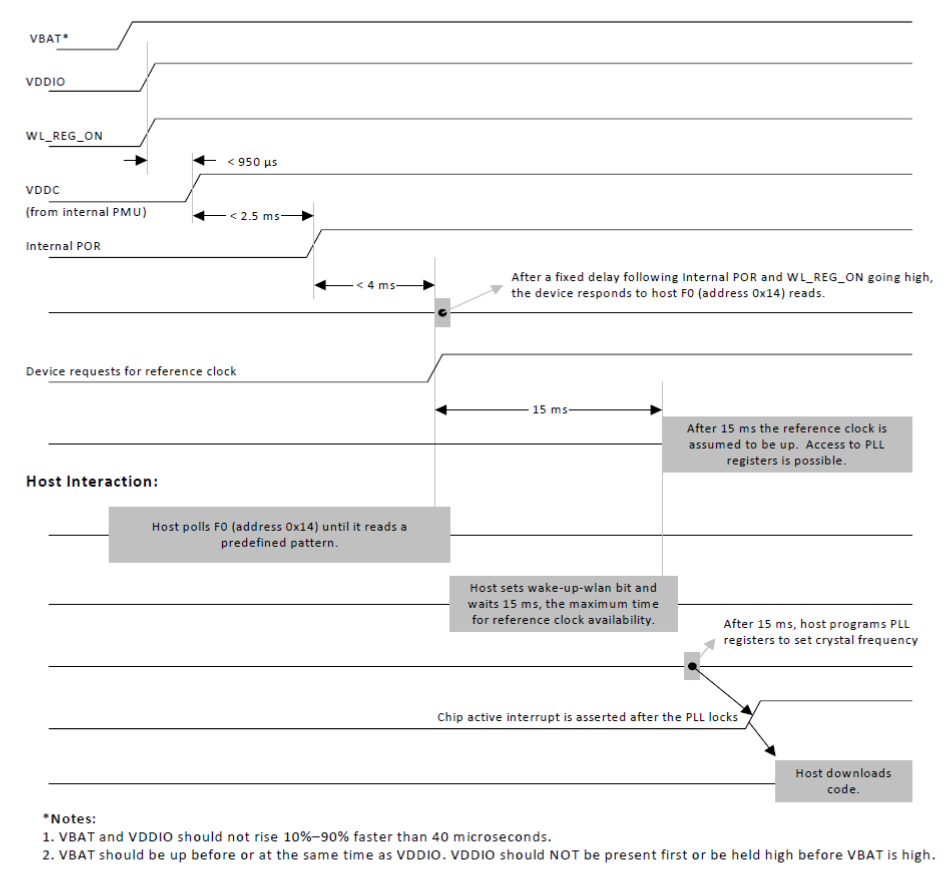
The CYW4373E has an internal power-on reset (POR) circuit. The device is held in reset for a maximum of 110 milliseconds after VDDC and VDDIO have passed the POR threshold. Wait at least 150 milliseconds after VDDC and VDDIO are available before initiating SDIO accesses.
VBAT should not rise 10%–90% faster than 40 microseconds. VBAT should be up before or at the same time as VDDIO. VDDIO should NOT be present first or be held high before VBAT is high.
Control Signal Timing Diagrams
WLAN=ON; Bluetooth=ON
WLAN=OFF; Bluetooth=OFF
WLAN=ON; Bluetooth=OFF
WLAN=OFF; Bluetooth=ON
WLAN Boot up Sequence for SDIO Host
Hardware Architecture
Block Diagrams
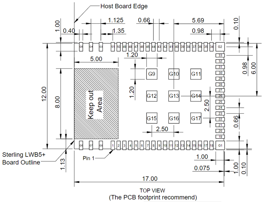
Pin-Out
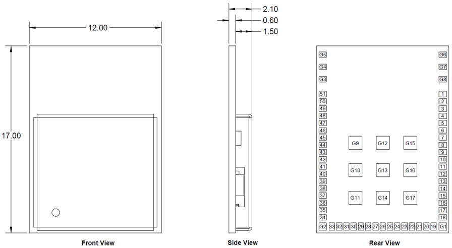
| Pin # | Name | Type | Pins Map to Chip | Voltage Ref. | Function | If Not Used |
|---|---|---|---|---|---|---|
| 1 | GND | - | - | - | Ground | GND |
| 2 | RF_SW_CTRL_5 | O | F10 | VDDIO _RF | RF switch control signal for Antenna diversity (only for trace pad variant) | NC |
| 3 | RF_SW_CTRL_0 | O | D10 | VDDIO _RF | RF switch control signal for Antenna diversity (only for trace pad variant) | NC |
| 4 | STRAP_2 | I | G7 | VDDIO | Strapping options to define Host interface, see Table 37 | -- |
| 5 | STRAP_0 | I | F7 | VDDIO | Strapping options to define Host interface, see Table 37 | -- |
| 6 | VOUT_3P3 | PWR O/P | - | VOUT _3P3 | Internal Regulator 3.3V output. If VBAT is 3.6V or greater, this power source should be used for VDDIO_RF, and USB2_AVDD33 if strapped for USB. Otherwise leave this pin disconnected. | NC |
| 7 | VDDIO_RF | PWR I/P | - | VDDIO _RF | DC supply voltage for RF switch IO’s. If VBAT is 3.6V or greater, connect to VOUT_3P3. Otherwise connect to VBAT. | -- |
| 8 | GND | - | - | - | Ground | GND |
| 9 | SDIO_DATA0 | I/O | B8 | VDDIO | SDIO data lin0 | NC |
| 10 | SDIO_DATA1 | I/O | C7 | VDDIO | SDIO data lin1 | NC |
| 11 | SDIO_DATA3 | I/O | B7 | VDDIO | SDIO data lin3 | NC |
| 12 | SDIO_CMD | I/O | C6 | VDDIO | SDIO command line | NC |
| 13 | SDIO_DATA2 | I/O | B6 | VDDIO | SDIO data lin2 | NC |
| 14 | GND | - | - | - | Ground | GND |
| 15 | SDIO_CLK | I | A6 | VDDIO | SDIO clock input | NC |
| 16 | GND | - | - | - | Ground | GND |
| 17 | VBAT | PWR I/P | - | VBAT | DC supply voltage for module. Operational: VBAT is 3.2V to 4.8V (See VDDIO_RF configuration) ** VBAT at 3.6V to 4.8V has the same TX power but a better EVM/harmonic emissions margin. | -- |
| 18 | VBAT | PWR I/P | - | VBAT | DC supply voltage for module. Operational: VBAT is 3.2V to 4.8V (See VDDIO_RF configuration) ** VBAT at 3.6V to 4.8V has the same TX power but a better EVM/harmonic emissions margin. | -- |
| Note: VBAT should not rise 10%-90% faster than 40 microseconds. VBAT should be up before or at the same time as VDDIO. VDDIO should not be present first or be held high before VBAT is high. | ||||||
| G1 | GND | - | - | - | Ground | GND |
| 19 | GPIO_4 | I | D3 | VDDIO | Reserved for feature support WCI-2 LTE coexistence Interface | NC |
| 20 | GPIO_6 | O | E4 | VDDIO | Reserved for feature support 3-wire external coexistence interface. TX_CONF: Grant of access indication to external device. | NC |
| 21 | GPIO_3 | I | D2 | VDDIO | Reserved for feature support 3-wire external coexistence interface. STATUS: Indicates priority and TX/RX. | NC |
| 22 | GPIO_2 | I | E1 | VDDIO | Reserved for feature support 3-wire external coexistence interface. RF_ACTIVE: Request indication from external device for access | NC |
| 23 | GPIO_5 | O | E3 | VDDIO | Reserved for feature support WCI-2 LTE coexistence Interface | NC |
| 24 | USB2_DM | I/O | F1 | - | Data minus of shared USB 2.0 port | NC |
| 25 | USB2_DP | I/O | G1 | - | Data plus of shared USB 2.0 port | NC |
| 26 | USB2_RREF | I/O | H1 | - | Bandgap reference resistor. When in SDIO interface, leave open. When in USB interface, connect to ground through 4.75K Ohm 1%. | -- |
| 27 | GND | - | - | - | Ground | GND |
| 28 | USB2_AVDD33 | PWR | H2 | VBAT | In SDIO interface, short to Ground. In USB interface, If VBAT is 3.6V or greater, connect to VOUT_3P3. Otherwise connect to VBAT. | -- |
| 29 | GND | - | - | - | Ground | GND |
| 30 | VDDIO | PWR | - | - | WLAN/BT IO Voltage (1.8V/3.3V). | -- |
| 31 | GPIO_1 | I/O | D1 | VDDIO | Reserved for feature support Reserved for WL_DEVICE_WAKE. Input from Host to wake up WLAN module. | NC |
| 32 | BT_REG_ON | I | C3 | VDDIO | Enables Bluetooth regulators. Internal 100K pull-up to enable Bluetooth by default. Ground to disable Bluetooth. | NC |
| 33 | WL_REG_ON | I | D4 | VDDIO | Enables WLAN regulators. Internal 100K pull-up to enable WLAN by default. Ground to disable WLAN. | NC |
| G2 | GND | - | - | - | Ground | GND |
| 34 | SUSCLK | I | J2 | 200mVp-p to 3300mVp-p | External Sleep Clock input (32.768KHz) Externally provided sleep clock is required | -- |
| 35 | GND | - | - | Ground | GND | |
| 36 | GPIO_0 | I/O | F3 | VDDIO | Reserved for feature support Reserved for WL_HOST_WAKE. Output signal to wake up host. | NC |
| 37 | BT_DEVICE _WAKE | I | L2 | VDDIO | Reserved for feature support BT_DEVICE_WAKE. Input signal from Host. | NC |
| 38 | BT_PCM_IN | I | J1 | VDDIO | PCM data input. | NC |
| 39 | BT_PCM_CLK | I/O | K1 | VDDIO | PCM clock. Can be master (Output) or slave (Input) | NC |
| 40 | BT_PCM_SYNC | I/O | K3 | VDDIO | PCM Sync. Can be master (Output) or slave (Input); Or SLIMbus data. | NC |
| 41 | BT_PCM_OUT | O | L3 | VDDIO | PCM data output. | NC |
| 42 | GND | - | - | Ground | GND | |
| 43 | BT_UART_TXD | O | M1 | VDDIO | Serial data output for the HCI UART interface. | NC |
| 44 | BT_UART_CTSn | I | M2 | VDDIO | Active-Low clear-to-send signal for the HCI UART interface. | NC |
| 45 | BT_UART_RXD | I | N2 | VDDIO | Serial data input for the HCI UART interface. | NC |
| 46 | BT_UART_RTSn | O | N3 | VDDIO | Active-Low request-to-send signal for the HCI UART interface. | NC |
| 47 | BT_HOST_WAKE | O | M3 | VDDIO | Reserved for feature support BT_HOST_WAKE. Output signal to wake up Host. | NC |
| 48 | GND | - | - | - | Ground | GND |
| 49 | GND | - | - | - | Ground | GND |
| 50 | RF_OUT | - | - | - | RF output pin for the LWB5+ “ST” variant. For “SA” or “SC” variants, it is no connection. SC - MHF4 connector (00046) ST - Trace (00047) | NC |
| 51 | GND | - | - | - | Ground | GND |
| G3-G17 | GND | - | - | - | Ground | GND |
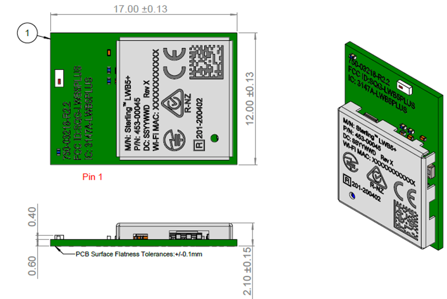
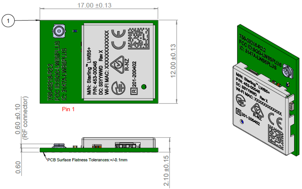
Mechanical Drawings
Module dimensions of LWB5+ series wireless module is 17 x 12 x 2.1 mm.
453-00045
453-00046
453-00047
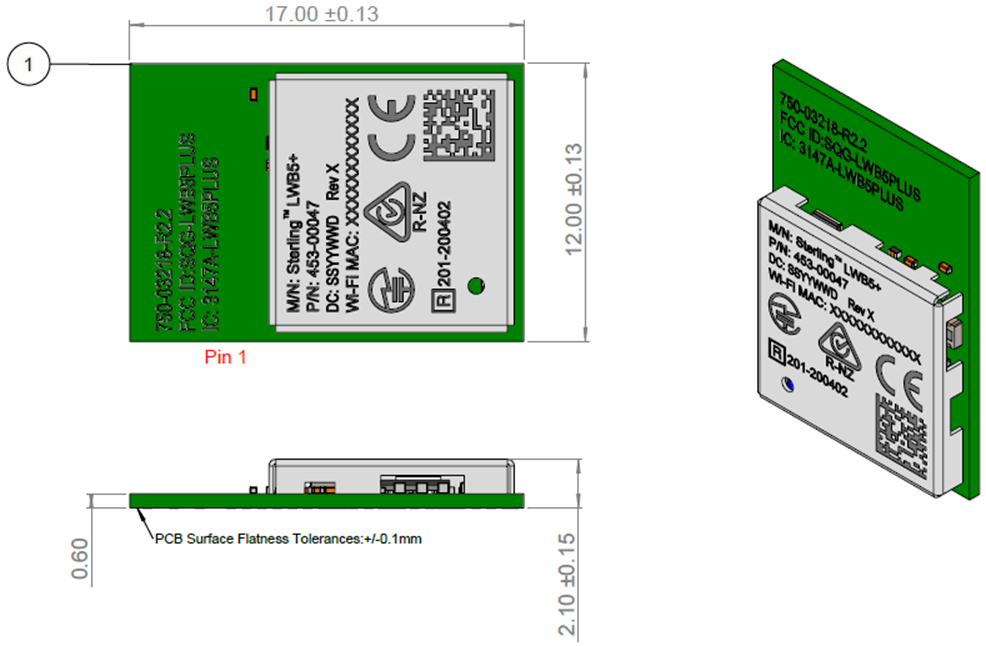
Notes:
The Wi-Fi MAC address is located on the product label.
The last digit of Wi-Fi MAC address is assigned to either 0, 2, 4, 6, 8, A, C, E.
The Bluetooth MAC address is the Wi-Fi MAC address plus 1.
Host Interface Specifications
Host Configuration Options
LWB5+ series wireless module supports various host configurations for WLAN and Bluetooth.
| Strap Value CONFIG_HOST [2-0] | WLAN | Bluetooth/BLE | Notes |
|---|---|---|---|
| 000 | USB | USB | USB2.0 |
| 101 | SDIO | UART | SDIO 1.8V (Supports DS/HS and SDR speed modes) |
| 100 | SDIO | UART | SDIO 3.3V (Supports DS and HS speed modes only) |
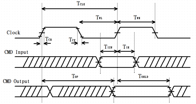
SDIO Specifications
The LWB5+ series wireless module SDIO host interface pins are powered from the VIO_SD voltage supply. The SDIO electrical specifications are identical for the 1-bit SDIO and 4-bit SDIO modes.
Default Speed, High-speed Modes
Note: Over full range of values specified in the Recommended Operating Conditions unless otherwise specified.
SDIO timing requirements are listed below.
| Symbol | Parameter | Condition | Min. | Typ. | Max. | Unit |
|---|---|---|---|---|---|---|
| fPP | Clock Frequency | Default Speed High-Speed | 0 0 | - - | 25 50 | MHz |
| TWL | Clock low time | Default Speed High-Speed | 10 7 | - - | - - | ns |
| TWH | Clock high time | Default Speed High-Speed | 10 7 | - - | - - | ns |
| TISU | Input Setup time | Default Speed High-Speed | 5 6 | - - | - - | ns |
| TIH | Input Hold time | Default Speed High-Speed | 5 2 | - - | - - | ns |
| TODLY | Output delay time CL≦40pF (1 card) | Default Speed High-Speed | - - | - - | 14 14 | ns |
| TOH | Output hold time | High-Speed | 0 | - | - | ns |
SDR12, SDR25, SDR50 Mode (up to 100 MHz) (1.8V)
Note: Over full range of values specified in the Recommended Operating Conditions unless otherwise specified.
SDIO timing requirements--- SDR12, SDR25, SDR50 modes (up to 100 MHz) (1.8V) are listed below.
| Symbol | Parameter | Condition | Min. | Typ. | Max. | Unit |
|---|---|---|---|---|---|---|
| fPP | Clock Frequency | SDR12/25/50 | 25 | - | 100 | MHz |
| TISU | Input setup time | SDR12/25/50 | 3 | -- | - | ns |
| TIH | Input Hold time | SDR12/25/50 | 0.8 | - | - | ns |
| TCLK | Clock Time | SDR12/25/50 | 10 | - | 40 | ns |
| TCR, TCF | Raise time, Fall time TCR, TCF <2ns (max) at 100MHz CCARD=10pF | SDR12/25/50 | - | - | 0.2*TCLK | ns |
| TODLY | Output delay time CL≦30pF | SDR12/25/50 | - | - | 7.5 | ns |
| TOH | Output hold time CL=15pF | SDR12/25/50 | 1.5 | - | - | ns |
SDR104 Mode (208 MHz) (1.8V)
Note: Over full range of values specified in the Recommended Operating Conditions unless otherwise specified.
SDIO timing requirements -- SDR104 modes (up to 208MHz) (1.8V) are listed below.
| Symbol | Parameter | Condition | Min. | Typ. | Max. | Unit |
|---|---|---|---|---|---|---|
| fPP | Clock Frequency | SDR104 | 0 | - | 208 | MHz |
| TISU | Input setup time | SDR104 | 1.4 | -- | - | ns |
| TIH | Input Hold time | SDR104 | 0.8 | - | - | ns |
| TCLK | Clock Time | SDR104 | 4.8 | - | - | ns |
| TCR, TCF | Raise time, Fall time TCR, TCF <0.96ns (max) at 208MHz CCARD=10pF | SDR104 | - | - | 0.2*TCLK | ns |
| TOP | Card Output phase | SDR104 | 0 | - | 10 | ns |
| TODW | Output timing pf variable data window | SDR12/25/SDR50 | 2.88 | - | - | ns |
DDR50 Mode (50 MHz) (1.8V)
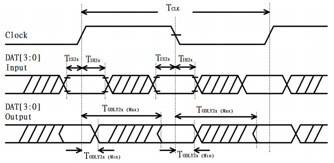
Note: In DDR50 mode, DAT[3:0] lines are samples on both edges of the clock (not applicable for CMD line)
SDIO timing requirements – DDR50 modes (50 MHz) are listed below.
| Symbol | Parameter | Condition | Min. | Typ. | Max. | Unit | |
|---|---|---|---|---|---|---|---|
| Clock | |||||||
| TCLK | Clock time 50MHz (max) between rising edge | DDR50 | 20 | -- | -- | ns | |
| TCR, TCF | Rise time, fall time TCR, TCF <4.00ns (max) at 50MHz. CCARD=10pF | DDR50 | -- | -- | 0.2*TCLK | ns | |
| Clock Duty | -- | DDR50 | 45 | -- | 55 | % | |
| CMD Input (referenced to clock rising edge) | |||||||
| TIS | Input setup time CCARD≦10pF (1 card) | DDR50 | 6 | -- | -- | ns | |
| TIH | Input hold time CCARD≦10pF (1 card) | DDR50 | 0.8 | -- | -- | ns | |
| CMD Output (referenced to clock rising and failing edge) | |||||||
| TODLY | Output delay time during data transfer mode CL≦30pF (1 card) | DDR50 | -- | -- | 13.7 | ns | |
| TOHLD | Output hold time CL≥15pF (1 card) | DDR50 | 1.5 | -- | -- | ns | |
| DAT[3:0] Input (referenced to clock rising and failing edges) | |||||||
| TIS2X | Input setup time CCARD≦10pF (1 card) | DDR50 | 3 | -- | -- | ns | |
| TIH2X | Input hold time CCARD≦10pF (1 card) | DDR50 | 0.8 | -- | -- | ns | |
| DAT[3:0] Output (referenced to clock rising and failing edges) | |||||||
| TODLY2X (max) | Output delay time during data transfer mode CL≦25pF (1 card) | DDR50 | -- | -- | 7.0 | ns | |
| TODLY2X (min) | Output hold time CL≥15pF (1 card)) | DDR50 | 1.5 | -- | -- | ns | |
USB Specifications
USB LS Driver and Receiver Parameters
Notes:
Over full range of values specified in the Recommended Operating Conditions unless otherwise specified.
The load is 100Ω differential for these parameters, unless other specified.
| Symbol | Parameter | Min. | Typ. | Max. | Unit | |
|---|---|---|---|---|---|---|
| BR | Baud rate | - | 1.5 | - | Mbps | |
| BRPPM | Baud rate tolerance | -15000 | - | 15000 | ppm | |
| Driver Specifications | ||||||
| VOH | Output signal ended high Defined with 1.425KΩ pull-up resistor to 3.6V | 2.8 | - | 3.6 | V | |
| VOL | Output signal ended low Defined with 1.425KΩ pull-up resistor to ground | 0.0 | - | 0.3 | V | |
| VCRS | Output signal crossover voltage | 1.3 | 2.0 | V | ||
| TLR | Data fall time Defined from 10% to 90% for raise time and 90% to 10% for fall time | 75.0 | - | 300.0 | ns | |
| TLF | Data rise time Defined from 10% to 90% for raise time and 90% to 10% for fall time | 75.0 | - | 300.0 | ns | |
| TLRFM | Rise and fall time matching | 80.0 | - | 125.0 | % | |
| TUDJ1 | Source jitter total: to next transition *Including frequency tolerance. Timing difference between the differential data signals. *Defined at crossover point of differential signals | -95 | - | 95 | ns | |
| TUDJ2 | Source jitter total: for paired transitions *Including frequency tolerance. Timing difference between the differential data signals. *Defined at crossover point of differential signals | -150 | - | 150 | ns | |
| Receiver Specifications | ||||||
| VIH | Input signal ended high | 2.0 | - | - | V | |
| VIL | Input signal ended low | - | - | 0.8 | V | |
| VDI | Differential input sensitivity | 0.2 | - | - | V | |
USB FS Driver and Receiver Parameters
Notes:
Over full range of values specified in the Recommended Operating Conditions unless otherwise specified.
The load is 100Ω differential for these parameters, unless other specified.
| Symbol | Parameter | Min. | Typ. | Max. | Unit |
|---|---|---|---|---|---|
| BR | Baud rate | - | 12.0 | - | Mbps |
| BRPPM | Baud rate tolerance | -2500 | - | 2500 | ppm |
| Driver Specifications | |||||
| VOH | Output signal ended high Defined with 1.425KΩ pull-up resistor to 3.6V | 2.8 | - | 3.6 | V |
| VOL | Output signal ended low Defined with 1.425KΩ pull-up resistor to ground | 0.0 | - | 0.3 | V |
| VCRS | Output signal crossover voltage | 1.3 | 2.0 | V | |
| TFR | Output raise time Defined from 10% to 90% for raise time and 90% to 10% for fall time | -4.0 | - | 20.0 | ns |
| TFL | Output fall time Defined from 10% to 90% for raise time and 90% to 10% for fall time | -4.0 | - | 20.0 | ns |
| TDJ1 | Source jitter total: to next transition *Including frequency tolerance. Timing difference between the differential data signals. *Defined at crossover point of differential signals | -3.5 | - | 3.5 | ns |
| TDJ2 | Source jitter total: for paired transitions *Including frequency tolerance. Timing difference between the differential data signals. *Defined at crossover point of differential signals | -4.0 | - | 4.0 | ns |
| TFDEOP | Source jitter for differential transition to SE0 transition. Defined at crossover point of differential signals | -2.0 | - | 5.0 | ns |
| Receiver Specifications | |||||
| VIH | Input signal ended high | 2.0 | - | - | V |
| VIL | Input signal ended low | - | - | 0.8 | V |
| VDI | Differential input sensitivity | 0.2 | - | - | V |
| TJR1 | Receiver jitter: to next transition Defined at crossover point of differential data signals | -18.5 | - | 18.5 | ns |
| TJR2 | Receiver jitter: for paired transitions Defined at crossover point of differential data signals | -9.0 | - | 9.0 | ns |
USB HS Driver and Receiver Parameters
Notes:
Over full range of values specified in the Recommended Operating Conditions unless otherwise specified.
The load is 100Ω differential for these parameters, unless other specified.
| Symbol | Parameter | Min. | Typ. | Max. | Unit |
|---|---|---|---|---|---|
| BR | Baud rate | - | 480 | - | Mbps |
| BRPPM | Baud rate tolerance | -500 | - | 500 | ppm |
| Driver Specifications | |||||
| VHSOH | Data signal high | 360 | - | 440 | mV |
| VHSOL | Data signal low | -10 | - | 10 | mV |
| THSR | Data rise time Defined from 10% to 90% for raise time and 90% to 10% for fall time | 500 | - | - | ns |
| THSF | Data fall time Defined from 10% to 90% for raise time and 90% to 10% for fall time | -500 | - | - | ns |
| Receiver Specifications | |||||
| VHSCM | Input signal ended low | -50 | - | 500 | mV |
PCM Interface Specifications
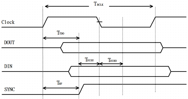
| Symbol | Parameter | Min. | Typ. | Max. | Unit |
|---|---|---|---|---|---|
| FBCLK | - | - | 2/2.048 | - | MHz |
| Duty CycleBCLK | - | 0.4 | 0.5 | 0.6 | - |
| TBCLK rise/fall | - | - | 3 | - | ns |
| TDO | - | - | - | 15 | ns |
| TDISU | - | 20 | - | - | ns |
| TDIHO | - | 15 | - | - | ns |
| TBF | - | - | - | 15 | ns |
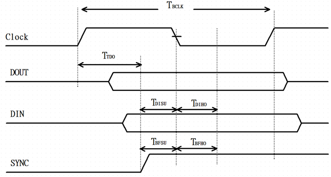
| Symbol | Parameter | Min. | Typ. | Max. | Unit |
|---|---|---|---|---|---|
| FBCLK | - | - | 2/2.048 | - | MHz |
| Duty CycleBCLK | - | 0.4 | 0.5 | 0.6 | - |
| TBCLK rise/fall | - | - | 3 | - | ns |
| TDO | - | - | - | 30 | ns |
| TDISU | - | 15 | - | - | ns |
| TDIHO | - | 10 | - | - | ns |
| TBFSU | - | 15 | - | - | ns |
| TBFHO | - | 10 | - | - | ns |
Electrical Characteristics
Absolute Maximum Ratings
The following table summarizes the absolute maximum ratings for the LWB5+ series wireless module. Absolute maximum ratings are those values beyond which damage to the device can occur. Functional operation under these conditions, or at any other condition beyond those indicated in the operational sections of this document, is not recommended.
Note: Maximum rating for signals follows the supply domain of the signals.
| Symbol (Domain) | Parameter | Max Rating | Unit |
|---|---|---|---|
| VDDIO | WLAN host SDIO interface I/O supply (for 1.8V system) (for 3.3V system) | 2.2 4.0 | V |
| VDDIO_RF | I/O configuration power supply (for 3.3V system) | 4.0 | V |
| VBAT | External DC power supply | 5.0 | V |
| Storage | Storage temperature | -40 to +85 | °C |
| Antenna | Maximum RF input (reference to 50-Ω input) | +10 | dBm |
| ESD | Electrostatic discharge tolerance | 2000 | V |
Recommended Operating Conditions
The following table lists the recommended operating conditions for the LWB5+ series wireless module.
| Symbol (Domain) | Parameter | Min | Typ | Max | Unit |
|---|---|---|---|---|---|
| VDDIO | WLAN and Bluetooth host interface I/O supply | 1.62/2.97 | 1.8/3.3 | 1.98/3.63 | V |
| VDDIO_RF | I/O supply for the RF switch control pads | 3.2 | 3.3 | 3.63 | V |
| VBAT | External DC power supply | 3.2 | 3.30 | 3.63 | V |
| EVM/harmonics are improved | 3.6 | — | 4.8 | V | |
| T-ambient | Ambient temperature | -40 | 25 | 85 | °C |
DC Electrical Characteristics
The following tables list the general DC electrical characteristics over recommended operating conditions (unless otherwise specified).
General DC electrical characteristics (For 1.8V operation VDDIO)
| Symbol | Parameter | Conditions | Min | Typ | Max | Unit |
|---|---|---|---|---|---|---|
| VIH | High Level Input Voltage | — | 1.17 | — | — | V |
| VIL | Low Level Input Voltage | — | — | — | 0.63 | V |
| VOH | Output high Voltage | — | 1.35 | — | — | V |
| VOL | Output low Voltage | — | — | — | 0.45 | V |
General DC electrical characteristics (For 3.3V operation VIO_SD; VIO)
| Symbol | Parameter | Conditions | Min | Typ | Max | Unit |
|---|---|---|---|---|---|---|
| VIH | High Level Input Voltage | — | 2.0 | — | — | V |
| VIL | Low Level Input Voltage | — | — | — | 0.8 | V |
| VOH | Output high Voltage | — | 2.9 | — | — | V |
| VOL | Output low Voltage | — | — | — | 0.4 | V |
Current Consumption
WLAN current consumption on 2.4 GHz (SDIO=VDIO=3.3V)
| Freq. | Mode/Rate (Mbps) | Output Power (dBm) | Maximum Current Consumption (mA)8 |
|---|---|---|---|
2412 MHz 2422 MHz | 1 Mbps | 18 dBm | 369 |
| 54 Mbps | 18 dBm | 365 | |
| HT20 MCS7 | 17.5 dBm | 351 | |
| HT40 MCS7 | 16.5 dBm | 342 | |
| 2442 MHz | 1 Mbps | 18 dBm | 369 |
| 54 Mbps | 17 dBm | 365 | |
| HT20 MCS7 | 17 dBm | 351 | |
| HT40 MCS7 | 16 dBm | 342 | |
2472 MHz 2462 MHz | 1 Mbps | 18 dBm | 369 |
| 54 Mbps | 17 dBm | 365 | |
| HT20 MCS7 | 17 dBm | 351 | |
| HT40 MCS7 | 16 dBm | 342 |
2 GHz WLAN sleep mode current
| Mode | VBAT = 3.6V, VDDIO = 1.8V, TA = 25°C VBAT, mA | VBAT = 3.6V, VDDIO = 1.8V, TA = 25°C VIO, uA1 |
| Sleep Modes (SDIO Interface) | ||
| OFF2 | 0.003 | 0.15 |
| Sleep3 | 0.03 | 200 |
| Sleep Modes (USB Interface) | ||
| OFF2 | 0.003 | 0.057 |
| Sleep3 | 0.49 | 230 |
[1] VIO is specified with all pins idle (not switching) and not driving any loads. [2] WL_REG_ON and BT_REG_ON are both low. All supplies present. [3] Idle, not associated, or inter-beacon. | ||
WLAN transmitter characteristics for 5 GHz operation (SDIO=VDDIO=3.3V)
| Symbol | Parameter | Conditions | Min | Typ | Max | Unit |
|---|---|---|---|---|---|---|
| Ftx | Transmit output frequency range | — | 5.15 | — | 5.925 | GHz |
| Pout | Output power | See Note2 | — | — | — | — |
| 11a mask compliant | 6-36Mbps | — | 17.5 | — | dBm | |
| 11a EVM compliant | 48-54Mbps | — | 17.5 | — | ||
| 11n HT20 mask compliant | MCS0-5 | — | 17.5 | — | ||
| 11n HT20 EVM compliant | MCS6-7 | — | 16.5 | — | ||
| 11n HT40 mask compliant | MCS0-5 | — | 17.5 | — | ||
| 11n HT40 EVM compliant | MCS6-7 | — | 16 | — | ||
| 11ac VHT20 mask compliant | MCS0-5 | — | 17.5 | — | ||
| 11ac VHT20 EVM compliant | MCS6-8 | — | 15 | — | ||
| 11ac VHT40 mask compliant | MCS0-5 | — | 17.5 | — | ||
| 11ac VHT40 EVM compliant | MCS6-7 | — | 16 | — | ||
| 11ac VHT40 EVM compliant | MCS8-9 | — | 13.5 | — | ||
| 11ac VHT80 mask compliant | MCS0-5 | — | 17.5 | — | ||
| 11ac VHT80 EVM compliant | MCS6-7 | — | 16 | — | ||
| 11ac VHT80 EVM compliant | MCS8-9 | — | 13.5 | — | ||
| ATx | Transmit power accuracy at 25 ℃ | — | -2.0 | — | +2.0 | dB |
5 GHz WLAN sleep mode current
| Mode | VBAT = 3.6V, VDDIO = 1.8V, TA = 25°C VBAT, mA | VBAT = 3.6V, VDDIO = 1.8V, TA = 25°C VIO, µA1 |
|---|---|---|
| Sleep Modes (SDIO Interface) | ||
| OFF2 | 0.003 | 0.15 |
| Sleep3 | 0.03 | 200 |
| Sleep Modes (USB Interface) | ||
| OFF2 | 0.003 | 0.057 |
| Sleep3 | 0.49 | 230 |
[1] VIO is specified with all pins idle (not switching) and not driving any loads. [2] WL_REG_ON and BT_REG_ON are both low. All supplies present. [3] Idle, not associated, or inter-beacon. | ||
WLAN current consumption on 5 GHz (SDIO=VDDIO=3.3V)
| Frequency (MHz) | Mode/Rate (Mbps) | Output Power (dBm) | Maximum Current Consumption (mA) |
|---|---|---|---|
| 5180 | 6 Mbps | 17.5 | 370 |
| 54 Mbps | 17.5 | 354 | |
| HT20 MCS0 | 17.5 | 372 | |
| HT20 MCS7 | 16.5 | 350 | |
| 5190 | HT40 MCS0 | 17.5 | 410 |
| HT40 MCS7 | 16 | 377 | |
| 5210 | VHT80 MCS0 | 17.5 | 441 |
| VHT80 MCS9 | 13.5 | 352 | |
| 5500 | 6 Mbps | 17.5 | 370 |
| 54 Mbps | 17.5 | 354 | |
| HT20 MCS0 | 17.5 | 372 | |
| HT20 MCS7 | 16.5 | 350 | |
| 5510 | HT40 MCS0 | 17.5 | 410 |
| HT40 MCS7 | 16 | 377 | |
| 5530 | VHT80 MCS0 | 17.5 | 441 |
| VHT80 MCS9 | 13.5 | 352 | |
| 5825 | 6 Mbps | 17.5 | 370 |
| 54 Mbps | 17.5 | 354 | |
| HT20 MCS0 | 17.5 | 372 | |
| HT20 MCS7 | 16.5 | 350 | |
| 5795 | HT40 MCS0 | 17.5 | 410 |
| HT40 MCS7 | 16 | 377 | |
| 5775 | VHT80 MCS0 | 17.5 | 441 |
| VHT80 MCS9 | 13.5 | 352 |
Note2: Final TX power values on each channel are limited by regulatory requirements
Peak PHY Calibration Current
| Mode | VBAT = 3.3V, VDDIO = 1.8V, TA = 25°C VBAT, mA | VBAT = 3.3V, VDDIO = 1.8V, TA = 25°C VIO, µA |
|---|---|---|
| Unassociated (2.4 GHz) | 768 | 510 |
| Associated (2.4 GHz) | 748 | 560 |
| Unassociated (5 GHz) | 666 | 410 |
| Associated (5 GHz) | 664 | 390 |
Bluetooth and Bluetooth LE sleep current
| Operating Mode | VBAT | VDDIO | Unit |
|---|---|---|---|
| Sleep | 3.91 | 300.0 | µA |
Note:
[1] This sleep current consumption number and other average current consumption numbers in this table assume the UART interface for Bluetooth. Sleep current when using the USB interface is ~800 µA. Average current consumption numbers are therefore also expected to be higher when using the USB interface for Bluetooth.
Bluetooth current consumption, VBAT=VDDIO=3.3V
| Operating Mode | Tx | Rx | Unit |
|---|---|---|---|
| DH1 | 24.07 | 24.06 | mA |
| DH3 | 29.23 | 29.03 | mA |
| DH5 | 30.04 | 30.02 | mA |
| 2DH1 | 18.24 | 18.19 | mA |
| 2DH3 | 25.46 | 25.12 | mA |
| 2DH5 | 25.83 | 25.77 | mA |
| 3DH1 | 21.47 | 21.43 | mA |
| 3DH3 | 25.21 | 25.26 | mA |
| 3DH5 | 25.84 | 25.79 | mA |
| LE | 30.37 | 14.61 | mA |
Bluetooth current consumption, VBAT=3.3V, VDDIO=1.8V
| Operating Mode | Tx | Rx | Unit |
|---|---|---|---|
| DH1 | 23.62 | 23.57 | mA |
| DH3 | 28.57 | 28.54 | mA |
| DH5 | 29.62 | 29.62 | mA |
| 2DH1 | 17.65 | 17.77 | mA |
| 2DH3 | 24.06 | 24.07 | mA |
| 2DH5 | 25.11 | 25.12 | mA |
| 3DH1 | 20.91 | 20.87 | mA |
| 3DH3 | 24.42 | 24.72 | mA |
| 3DH5 | 25.34 | 25.29 | mA |
| LE | 30.04 | 14.19 | mA |
Radio Characteristics
WLAN Radio Receiver Characteristics
The following tables summarize the LWB5+ series wireless module receiver characteristics.
WLAN receiver characteristics for 2.4 GHz single chain operation
| Symbol | Parameter | Conditions | Min | Typ | Max | Unit |
|---|---|---|---|---|---|---|
| Frx | Receive input frequency range | — | 2.412 | — | 2.484 | GHz |
| Srf | Sensitivity | |||||
| CCK, 1 Mbps | See Note1 | — | -95 | — | dBm | |
| CCK, 11 Mbps | — | -90 | — | |||
| OFDM, 6 Mbps | — | -92 | — | |||
| OFDM, 54 Mbps | — | -75 | — | |||
| HT20, MCS0 | — | -91 | — | |||
| HT20, MCS7 | — | -73 | — | |||
| HT40, MCS0 | — | -90 | — | |||
| HT40, MCS7 | — | -71 | — | |||
| Radj | Adjacent channel rejection | |||||
| OFDM, 6 Mbps | See Note1 | 16 | 38 | — | dB | |
| OFDM, 54 Mbps | -1 | 20.4 | — | |||
| HT20, MCS0 | 16 | 33.3 | — | |||
| HT20, MCS7 | -2 | 13.7 | — | |||
Note1: Performance data are measured under signal chain operation.
WLAN receiver characteristics for 5 GHz single chain operation
| Symbol | Parameter | Conditions | Min | Typ | Max | Unit |
|---|---|---|---|---|---|---|
| Frx | Receive input frequency range | — | 5.15 | — | 5.825 | GHz |
| Srf | Sensitivity | |||||
| OFDM, 6 Mbps | See Note1 | — | -92 | — | dBm | |
| OFDM, 54 Mbps | — | -74 | — | |||
| HT20, MCS0 | — | -91 | — | |||
| HT20, MCS7 | — | -73 | — | |||
| HT40, MCS0 | — | -89 | — | |||
| HT40, MCS7 | — | -69 | — | |||
| VHT20, MCS0 | — | -90 | — | |||
| VHT20, MCS8 | — | -67 | — | |||
| VHT40, MCS0 | — | -89 | — | |||
| VHT40, MCS9 | — | -63 | — | |||
| VHT80, MCS0 | — | -85 | — | |||
| VHT80, MCS9 | — | -60 | — | |||
Radj [Difference between interfering and desired signal (20 MHz apart)] | Adjacent channel rejection | |||||
| OFDM, 6 Mbps | See Note1 | 16 | 31.7 | — | dB | |
| OFDM, 54 Mbps | -1 | 13.8 | — | |||
| OFDM, 65 Mbps | -2 | 8.4 | — | |||
Radj. [Difference between interfering and desired sinal (40 MHz apart)] | OFDM, 6 Mbps | See Note1 | 32 | 44.7 | — | dB |
| OFDM, 54 Mbps | 15 | 26.6 | — | |||
| OFDM, 65 Mbps | 14 | 26.8 | — | |||
Note1: Performance data are measured under signal chain operation.
WLAN Transmitter Characteristics
WLAN transmitter characteristics for 2.4 GHz operation (SDIO=VDIO=3.3V)
| Symbol | Parameter | Conditions | Min | Typ | Max | Unit |
|---|---|---|---|---|---|---|
| Ftx | Transmit output frequency range | — | 2.402 | — | 2.484 | GHz |
| Pout | Output power | See Note2 | — | — | — | — |
| 11b mask compliant | 1-11Mbps | — | 18 | — | dBm | |
| 11g mask compliant | 6-36Mbps | — | 18 | — | ||
| 11g EVM compliant | 48-54Mbps | — | 18 | — | ||
| 11n HT20 mask compliant | MCS0-6 | — | 18 | — | ||
| 11n HT20 EVM compliant | MCS7 | — | 17.5 | — | ||
| 11n HT40 mask compliant | MCS0-5 | — | 18 | — | ||
| 11n HT40 EVM compliant | MCS6-7 | — | 16.5 | — | ||
| ATx | Transmit power accuracy at 25 ℃ | — | -2.0 | — | +2.0 | dB |
Bluetooth Transmitter Characteristics
The following tables describe the basic rate transmitter performance, basic rate receiver performance, enhanced rate receiver performance, and current consumption conditions at 25°C.
Basic rate transmitter performance temperature at 25°C (3.3V)
| Test Parameter | Min | Typ | Max | BT Spec. | Unit | ||
|---|---|---|---|---|---|---|---|
| Maximum RF Output Power | GFSK | — | — | 7 | 0 ~ +20 | dBm | |
| π/4-DQPSK | — | 3 | — | ||||
| 8-DPSK | — | 3 | — | ||||
| Frequency Range | 2.4 | — | 2.4835 | 2.4 ≤ f ≤ 2.4835 | GHz | ||
| 20 dB Bandwidth | — | 919.5 | — | ≤ 1000 | KHz | ||
| Δf1avg Maximum Modulation | 140 | 155 | 175 | 140 < Δf1avg < 175 | KHz | ||
| Δf2max Minimum Modulation | 115 | 135 | — | ≥ 115 | KHz | ||
| Δf2avg/Δf1avg | — | 0.9 | — | ≥ 0.80 | — | ||
| Initial Carrier Frequency | — | ± 25 | ± 75 | ≤ ± 75 | KHz | ||
| Frequency Drift (DH1 packet) | — | ± 10 | ± 25 | ± 25 | KHz | ||
| Frequency Drift (DH3 packet) | — | ± 10 | ± 40 | ± 40 | KHz | ||
| Frequency Drift (DH5 packet) | — | ± 10 | ± 40 | ± 40 | KHz | ||
| Drift rate | — | 8 | 20 | 20 | KHz/50us | ||
| Adjacent Channel Power | F ≥ ± 3 MHz | — | -50 | — | < -40 | dBm | |
| F = ± 2 MHz | — | -46 | — | ≤ -20 | dBm | ||
| F = ± 1 MHz | — | -15 | — | N/A | dBm | ||
Basic rate receiver performance at (3.3V)
| Test Parameter | Min | Typ | Max | Bluetooth Spec. | Unit | |
|---|---|---|---|---|---|---|
| Sensitivity (1DH5) | BER ≤ 0.1% | — | -91 | — | ≤ -70 | dBm |
| Maximum Input | BER ≤ 0.1% | — | — | -20 | ≥ -20 | dBm |
| Interference Performance | Co-Channel | — | 9 | 11 | 11 | dB |
| C/I 1 MHz adjacent channel | — | -5.5 | 0 | 0 | dB | |
| C/I 2 MHz adjacent channel | — | -38 | -30 | -30 | dB | |
| C/I ≥ 3 MHz adjacent channel | — | -46 | -40 | -40 | dB | |
| C/I image channel | — | -25.5 | -9 | -9 | dB | |
| C/I 1-MHz adjacent to image channel | — | -39 | -20 | -20 | dB | |
Enhanced data rate receiver performance (3.3V)
| Test Parameter | Min | Typ | Max | Bluetooth Spec. | Unit | |
|---|---|---|---|---|---|---|
| Sensitivity (BER ≤ 0.01%) | π/4-DQPSK | — | -93 | — | ≤ -70 | dBm |
| 8-DPSK | — | -87 | — | ≤ -70 | dBm | |
| Maximum Input (BER ≤ 0.1%) | π/4-DQPSK | — | — | -20 | ≥ -20 | dBm |
| 8-DPSK | — | — | -20 | ≥ -20 | dBm | |
| C/I Co-Channel (BER ≤ 0.1%) | π/4-DQPSK | — | 10.5 | 13 | ≤ ±13 | dB |
| 8-DPSK | — | 17.5 | 21 | ≤ ±21 | dB | |
| C/I 1 MHz adjacent Channel | π/4-DQPSK | — | -6 | 0 | ≤ 0 | dB |
| 8-DPSK | — | -3 | 5 | ≤5 | dB | |
| C/I 2 MHz adjacent Channel | π/4-DQPSK | — | -38.5 | -30 | ≤ -30 | dB |
| 8-DPSK | — | -37.5 | -25 | ≤ -25 | dB | |
| C/I ≥ 3 MHz adjacent Channel | π/4-DQPSK | — | -47 | -40 | ≤ -40 | dB |
| 8-DPSK | — | -39.5 | -33 | ≤ -33 | dB | |
| C/I image channel | π/4-DQPSK | — | -24.5 | -7 | ≤ -7 | dB |
| 8-DPSK | — | -17 | 0 | ≤ 0 | dB | |
| C/I 1 MHz adjacent to image channel | π/4-DQPSK | — | -43 | -20 | ≤ -20 | dB |
| 8-DPSK | — | -37 | -13 | ≤ -13 | dB | |
Out-of-Band Blocking Performance (CW) BER ≤ 0.1% | 30-2000MHz | — | -10 | — | — | dBm |
| 2-2.399GHz | — | -27 | — | — | dBm | |
| 2.484-3GHz | — | -27 | — | — | dBm | |
| 3-12.75GHz | — | -10 | — | — | dBm | |
BLE RF Specifications (3.3V)
| Parameter | Conditions | Min | Typ | Max | Unit |
|---|---|---|---|---|---|
| Frequency range | — | 2402 | — | 2480 | MHz |
| Rx sensitivity3 | GFSK, 30.8% PER, 1Mbps | — | -94 | — | dBm |
| Tx power4 | — | — | — | 7 | dBm |
| Δf1 average | — | 225 | 255 | 275 | KHz |
| Δf2 maximum5 | — | 185 | 220 | — | KHz |
 ratio ratio | — | 0.8 | 0.95 | — | — |
Notes:
[3] Dirty Tx is Off.
[4] The Bluetooth LE TX power cannot exceed 10 dBm EIRP specification limit. The front-end losses and antenna gain/loss must be factored in so as not to exceed the limit.
[5] At least 99.9% of all Δf2 maximum frequency values recorded over 10 packets must be greater than 185 KHz.
Integration Guidelines
Integrated Antenna Characteristics
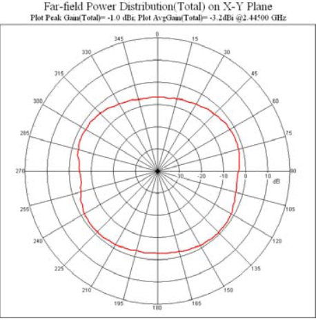
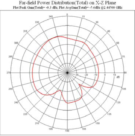
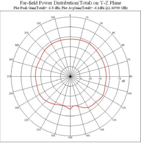
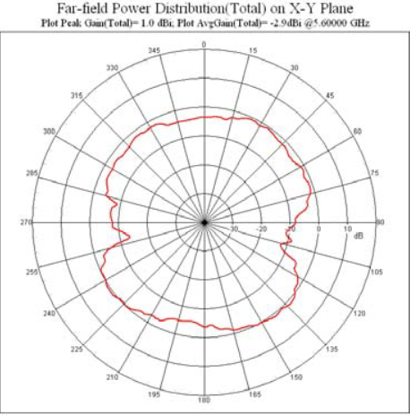
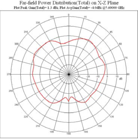
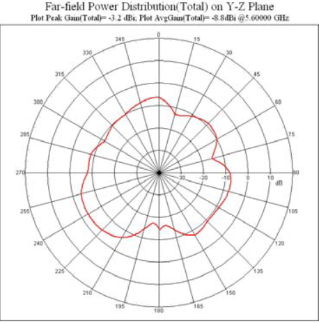
Summary of Antenna Performance
| Unit in dBi | XY-plane Peak | XY-plane Avg. | XZ-plane Peak | XZ-plane Avg. | YZ-plane Peak | YZ-plane Avg. |
|---|---|---|---|---|---|---|
| @2445MHz | -1.0 | -3.2 | -0.3 | -5.6 | -1.8 | -4.1 |
| @5600MHz | 1.0 | -2.9 | 1.3 | -4.0 | -3.2 | -8.8 |
2.4GHz Radiated Pattern
5GHz Radiated Pattern
PCB Layout
The following is a list of RF layout design guidelines and recommendation when installing a Ezurio radio into your device:
- Do not run antenna cables directly above or directly below the radio.
- Do not place any parts or run any high-speed digital lines below the radio.
- If there are other radios or transmitters located on the device (such as a Bluetooth radio), place the devices as far apart from each other as possible. Also, make sure there is at least 25 dB isolation between these two antennas.
- Ensure that there is the maximum allowable spacing separating the antenna connectors on the Ezurio radio from the antenna. In addition, do not place antennas directly above or directly below the radio.
- Ezurio recommends the use of a double-shielded cable for the connection between the radio and the antenna elements.
- Be sure to put a 10 µF capacitor on each 3.3V power pin. Also, place that capacitor to the pin as close as possible to make sure the internal PMU works correctly.
- Use proper electro-static-discharge (ESD) procedures when installing the Ezurio radio module. To avoid negatively impacting Tx power and receiver sensitivity, do not cover the antennas with metallic objects or components
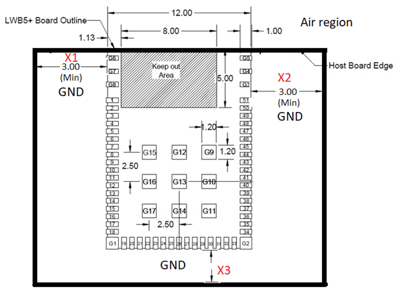
- The LWB5+ on-board antenna variant must be located at the edge of the host PCB surrounded by ground on three sides. A larger surround ground with X1, X2, X3 ≥ 15 millimeters has optimized performance. When X1, X2, X3 are reduced to 3 millimeters, the peak antenna gain drops to -3 dBi.
Application Note for Surface Mount Modules
Introduction
Ezurio’s surface mount modules are designed to conform to all major manufacturing guidelines. This application note is intended to provide additional guidance beyond the information that is presented in the user manual. This application note is considered a living document and will be updated as new information is presented.
The modules are designed to meet the needs of several commercial and industrial applications. They are easy to manufacture and conform to current automated manufacturing processes.
Shipping
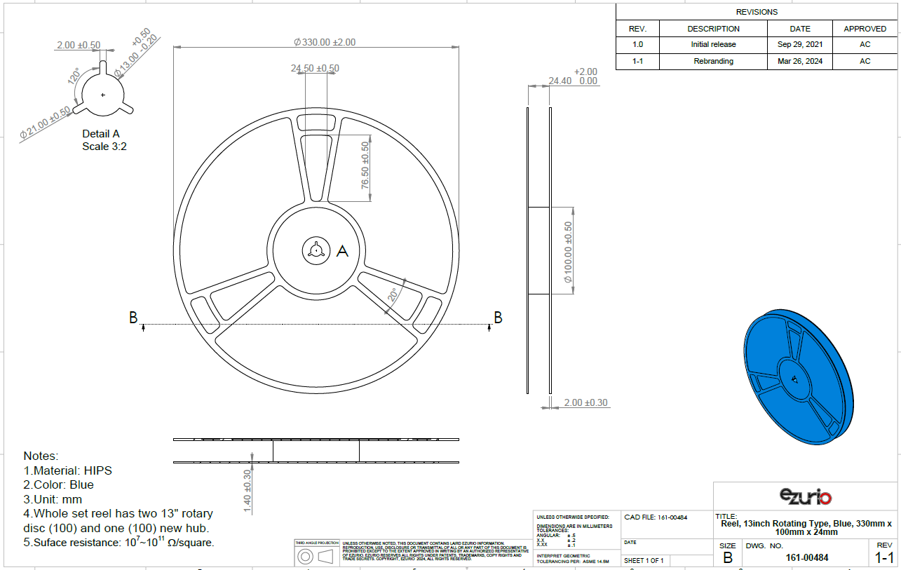
There are 1,000 Sterling LWB5+ modules taped in a reel (and packaged in a pizza box) and two boxes per carton (2000 modules per carton). Reel, boxes, and carton are labeled with the appropriate labels.
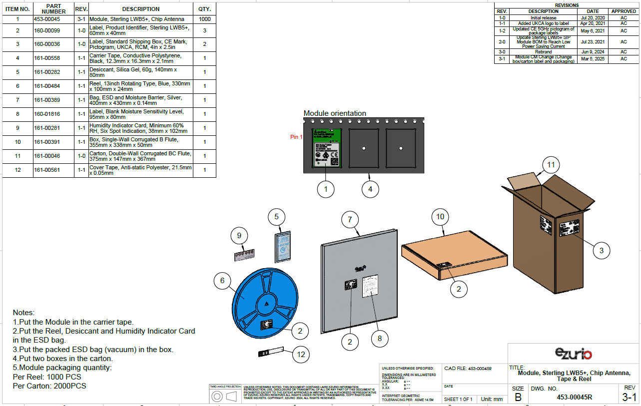
Labeling
The following labels are located on the antistatic bag and the box

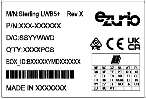
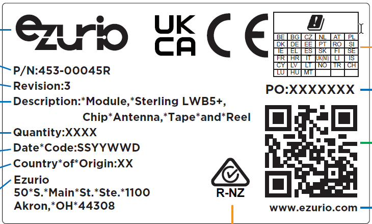
The following package label is located on adjacent sides of the master carton. (453-00045R example shown in below picture.)
Recommended Stencil Aperture
Note: When soldering, the stencil thickness should be ≥ 0.1 mm.
Reflow Parameters/ Soldering
Convection reflow or IR/Convection reflow (one-time soldering or two-time soldering in air or nitrogen environment)
- Measuring point – IC package surface
Temperature profile:
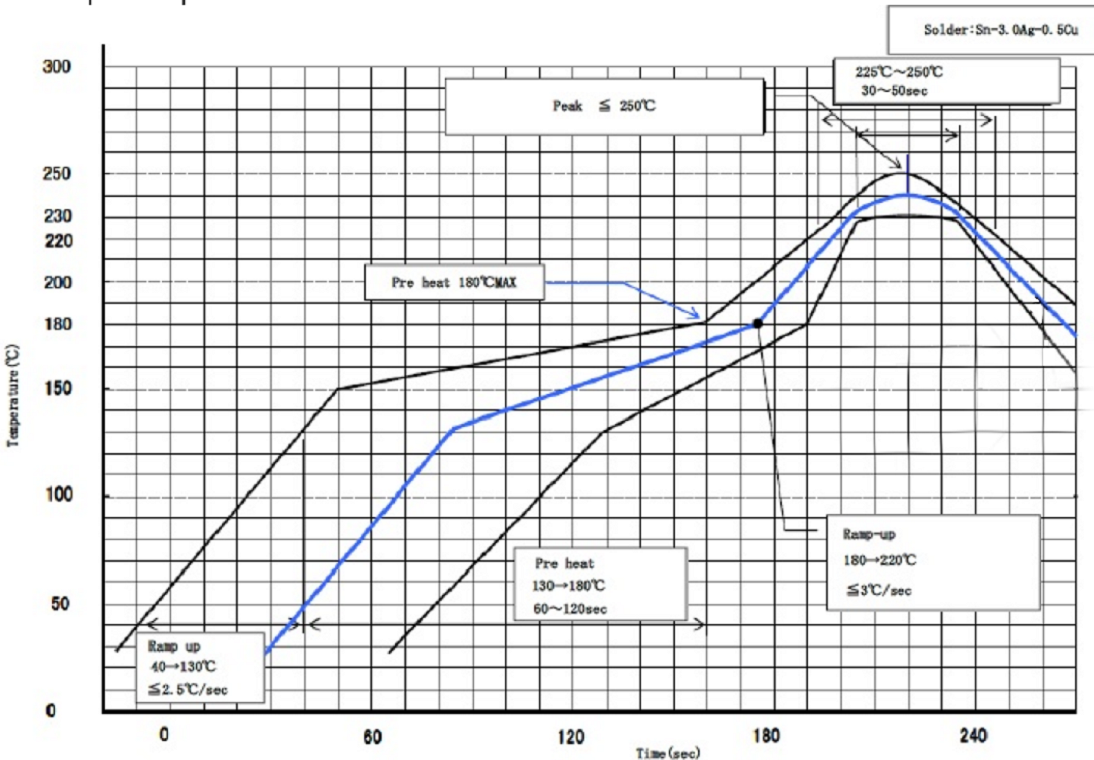
- Ramp-up: 40-130˚C. Less than 2.5˚C/sec
- Pre heat: 130-180˚C 60-120 sec, 180˚C MAX
- Ramp-up: 180-220˚C. Less than 3˚C/sec
Peak Temperature: MAX 250˚C
- 225˚C ~ 250˚C, 30 ~ 50 sec
- Ramp-down: Maximum 6˚C/sec
Cautions when Removing the SIP from the Platform for RMA
Cautions when Removing the SIP from the Platform for RMA
- Bake the platform before removing the module from the platform.
- Remove the module by using a hot air gun. This process should be carried out by a skilled technician.
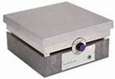
Recommended conditions for one-side component platform:
- Set the hot plate at 280°C.
- Put the platform on the hot plate for 8~10 seconds.
- Remove the device from platform.
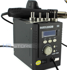
Recommended conditions for two-side components platform:
- Use two hot air guns.
- On the bottom, use a pre-heated nozzle (temp setting of 200~250°C) at a suitable distance from the platform PCB.
On the top, apply a remove nozzle (temp setting of 330°C). Heat until device can be removed from platform PCB.
- Remove the residue solder under the bottom side of device. (Note: Alternate module pictured as an example)
 |  |
| (Not accepted for RMA) | (Accepted for RMA analysis) |
- Remove and clean the residue flux as needed.
Precautions for Use:
- Opening/handling/removing must be done on an anti-ESD treated workbench. All workers must also have undergone anti-ESD treatment.
- The devices should be mounted within one year of the date of delivery.
- The LWB5+ modules are MSL level 4 rated.
Precautions for Use
Opening/handing/removing must be done on an anti-ESD treated workbench. All workers must also have undergone anti-ESD treatment.
The devices should be mounted within one year of the date of delivery.
The LWB5+ modules are MSL level 4
The Sona IF573 modules were tested for reliability as shown in Reliability Tests.
Environmental and Reliability
Environmental Requirements
Required Storage Conditions
Prior to Opening the Dry Packing
The following are required storage conditions prior to opening the dry packing:
- Normal temperature: 5~40˚C
- Normal humidity: 80% (Relative humidity) or less
- Storage period: One year or less
Note: Humidity means relative humidity.
After Opening the Dry Packing
The following are required storage conditions after opening the dry packing (to prevent moisture absorption):
Storage conditions for one-time soldering:
- Temperature: 5-25°C
- Humidity: 60% or less
- Period: 72 hours or less after opening
Storage conditions for two-time soldering
Storage conditions following opening and prior to performing the 1st reflow:
- Temperature: 5-25°C
- Humidity: 60% or less
- Period: A hours or less after opening
Storage conditions following completion of the 1st reflow and prior to performing the 2nd reflow
- Temperature: 5-25°C
- Humidity: 60% or less
- Period: B hours or less after completion of the 1st reflow
Note: Should keep A+B within 72 hours.
Temporary Storage Requirements after Opening
The following are temporary storage requirements after opening:
- Only re-store the devices once prior to soldering.
- Use a dry box or place desiccant (with a blue humidity indicator) with the devices and perform dry packing again using vacuumed heat-sealing.
The following indicate the required storage period, temperature, and humidity for this temporary storage:
Storage temperature and humidity:
*** - External atmosphere temperature and humidity of the dry packingStorage period:
- X1+X2 – Refer to After Opening the Dry Packing storage requirements. Keep is X1+X2 within 72 hours.
- Y – Keep within two weeks or less.
Baking Conditions
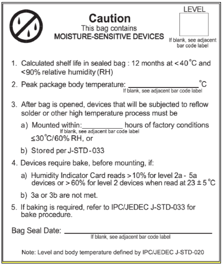
Baking conditions and processes for the module follow the J-STD-033 standard which includes the following:
- The calculated shelf life in a sealed bag is 12 months at <40℃ and <80% relative humidity.
- Once the packaging is opened, the SiP must be mounted (per MSL4/Moisture Sensitivity Level 4) within 72 hours at <30˚C and <60% relative humidity.
- If the SiP is not mounted within 72 hours or if, when the dry pack is opened, the humidity indicator card displays >10% humidity, then the product must be baked for 48 hours at 125 ˚C (±5 ˚C).
Reliability Tests
Environmental and Mechanical
| Test Item | Specification | Standard | Test Result |
|---|---|---|---|
| Step 1: Pre-conditioning | Pre-check:
Pre-conditioning:
Post-check:
| JESD22-A104 | Pass |
| Step 2: Temperature Cycling Non-operating |
| JESD22-A104 | Pass |
| Vibration Non-operating Unpackaged device |
| JEDEC 22-B103B (2016) | Pass |
Mechanical Shock Non-operating |
| JESD22-B104 | Pass |
Climatic and Dynamic
Reliability Prediction
| Test Item | Specification | Standard |
|---|---|---|
| Mean Time Between Failure (MTBF) |
| Telcordia SR-332 Issue 3 |
| Ezurio Part Number | Environment | Test Result -40°C (Hours) |
|---|---|---|
| 453-00045R 453-00045C 453-00046R 453-00046C 453-00047R 453-00047C | Ground, Fixed, Uncontrolled Ground, Mobile | 47,948,193.92 23,974,096.96 |
| Ezurio Part Number | Environment | Test Result 25°C (Hours) |
|---|---|---|
| 453-00045R 453-00045C 453-00046R 453-00046C 453-00047R 453-00047C | Ground, Fixed, Uncontrolled Ground, Mobile | 37,262,312.07 18,631,156.03 |
| Ezurio Part Number | Environment | Test Result 85 ℃ (Hours) |
|---|---|---|
| 453-00045R 453-00045C 453-00046R 453-00046C 453-00047R 453-00047C | Ground, Fixed, Uncontrolled Ground, Mobile | 1,496,189.35 748,094.67 |
| Ezurio Part Number | Environment | Test Result -40 ℃ (Hours) |
|---|---|---|
| 453-00048 453-00049 | Ground, Fixed, Uncontrolled Ground, Mobile | 15,549,723.4 7,774,861.7 |
| Ezurio Part Number | Environment | Test Result 25 ℃ (Hours) |
|---|---|---|
| 453-00048 453-00049 | Ground, Fixed, Uncontrolled Ground, Mobile | 13,788,688.76 6,894,344.38 |
| Ezurio Part Number | Environment | Test Result 85 ℃ (Hours) |
|---|---|---|
| 453-00048 453-00049 | Ground, Fixed, Uncontrolled Ground, Mobile | 962,576.28 481,288.14 |
Regulatory, Qualification & Certifications
Regulatory Approvals
For complete regulatory information, refer to the Sterling LWB5+ Regulatory Information document which is also available from the Sterling LWB5+ product page.
The Sterling LWB5+ holds current certifications in the following countries:
| Country/Region | Regulatory ID |
|---|---|
| USA (FCC) | SQG-LWB5PLUS |
| EU | N/A |
| Canada (ISED) | 3147A-LWB5PLUS |
| Japan (MIC) | 201-200402 |
| Australia | N/A |
| New Zealand | N/A |
Bluetooth SIG Qualification
The Bluetooth Qualification Process promotes global product interoperability and reinforces the strength of the Bluetooth® brand and ecosystem to the benefit of all Bluetooth SIG members. The Bluetooth Qualification Process helps member companies ensure their products that incorporate Bluetooth technology comply with the Bluetooth Patent & Copyright License Agreement and the Bluetooth Trademark License Agreement (collectively, the Bluetooth License Agreement) and Bluetooth Specifications.
The Bluetooth Qualification Process is defined by the Qualification Program Reference Document (QPRD) v3.
To demonstrate that a product complies with the Bluetooth Specification(s), each member must for each of its products:
- Identify the product, the design included in the product, the Bluetooth Specifications that the design implements, and the features of each implemented specification
- Complete the Bluetooth Qualification Process by submitting the required documentation for the product under a user account belonging to your company
The Bluetooth Qualification Process consists of the phases shown below:

To complete the Qualification Process the company developing a Bluetooth End Product shall be a member of the Bluetooth SIG. To start the application please use the following link: Apply for Adopter Membership
Scope
This guide is intended to provide guidance on the Bluetooth Qualification Process for End Products that reference multiple existing designs, that have not been modified, (refer to Section 3.2.2.1 of the Qualification Program Reference Document v3).
For a Product that includes a new Design created by combining two or more unmodified designs that have DNs or QDIDs into one of the permitted combinations in Table 3.1 of the QPRDv3, a Member must also provide the following information:
- DNs or QDIDs for Designs included in the new Design
- The desired Core Configuration of the new Design (if applicable, see Table 3.1 below)
- The active TCRL Package version used for checking the applicable Core Configuration (including transport compatibility) and evaluating test requirements
Any included Design must not implement any Layers using withdrawn specification(s).
When creating a new Design using Option 2a, the Inter-Layer Dependency (ILD) between Layers included in the Design will be checked based on the latest TCRL Package version used among the included Designs.
For the purposes of this document, it is assumed that the member is combining unmodified Core-Controller Configuration and Core-Host Configuration designs, to complete a Core-Complete Configuration.
Qualification Steps When Referencing multiple existing designs, (unmodified) – Option 2a in the QPRDv3
For this qualification option, follow these steps:
- To start a listing, go to: https://qualification.bluetooth.com/
- Select Start the Bluetooth Qualification Process.
Product Details to be entered:
- Project Name (this can be the product name or the Bluetooth Design name).
- Product Description
- Model Number
- Product Publication Date (the product publication date may not be later than 90 days after submission)
- Product Website (optional)
- Internal Visibility (this will define if the product will be visible to other users prior to publication)
- If you have multiple End Products to list then you can select ‘Import Multiple Products’, firstly downloading and completing the template, then by ‘Upload Product List’. This will populate Qualification Workspace with all your products.
Specify the Design:
- Do you include any existing Design(s) in your Product? Answer Yes, I do.
- Enter the multiple DNs or QDIDs used in your, (for Option 2a two or more DNs or QDIDs must be referenced)
- Select ‘I’m finished entering DN’s
- Once the DNs or QDIDs are selected they will appear on the left-hand side, indicating the layers covered by the design (should show Core-Controller and Core Host Layers covered).
- What do you want to do next? Answer, ‘Combine unmodified Designs’.
- The Qualification Workspace Tool will indicate that a new Design will be created and what type of Core-Complete configuration is selected.
- An active TCRL will be selected for the design.
- Perform the Consistency Check, which should result in no inconsistencies
- If there are any inconsistencies these will need to be resolved before proceeding
- Save and go to Test Plan and Documentation
Test Plan and Documentation
- As no modifications have been made to the combined designs the tool should report the following message:
‘No test plan has been generated for your new Design. Test declarations and test reports do not need to be submitted. You can continue to the next step.’ - Save and go to Product Qualification fee
- As no modifications have been made to the combined designs the tool should report the following message:
Product Qualification Fee:
- It’s important to make sure a Prepaid Product Qualification fee is available as it is required at this stage to complete the Qualification Process.
- Prepaid Product Qualification Fee’s will appear in the available list so select one for the listing.
- If one is not available select ‘Pay Product Qualification Fee’, payment can be done immediately via credit card, or you can pay via Invoice. Payment via credit will release the number immediately, if paying via invoice the number will not be released until the invoice is paid.
- Once you have selected the Prepaid Qualification Fee, select ‘Save and go to Submission’
Submission:
- Some automatic checks occur to ensure all submission requirements are complete.
- To complete the listing any errors must be corrected
- Once you have confirmed all design information is correct, tick all of the three check boxes and add your name to the signature page.
- Now select ‘Complete the Submission’.
- You will be asked a final time to confirm you want to proceed with the submission, select ‘Complete the Submission’.
- Qualification Workspace will confirm the submission has been submitted. The Bluetooth SIG will email confirmation once the submission has been accepted, (normally this takes 1 working day).
Download Product and Design Details (SDoC):
- You can now download a copy of the confirmed listing from the design listing page and save a copy in your Compliance Folder
For further information, please refer to the following webpage:
https://www.bluetooth.com/develop-with-bluetooth/qualification-listing/
Example Design Combinations
Ezurio Controller Subsystem + BlueZ 5.50 Host Stack (Ezurio Sterling LWB5+ based design)
| Design Name | Owner | Declaration ID | QD ID | Link to listing on the SIG website |
|---|---|---|---|---|
| Sterling LWB5+ | Ezurio | D050382 | 159315 | https://qualification.bluetooth.com/ListingDetails/119009 |
| BlueZ 5.50 Host Stack | Ezurio | D046330 | 138224 | https://qualification.bluetooth.com/ListingDetails/93911 |
Qualify More Products
If you develop further products based on the same design in the future, it is possible to add them free of charge. The new product must not modify the existing design i.e add ICS functionality, otherwise a new design listing will be required.
To add more products to your design, select ‘Manage Submitted Products’ in the Getting Started page, Actions, Qualify More Products. The tool will take you through the updating process.
Ordering Information
| Part Number | Description |
|---|---|
| 453-00045R | 1x1 802.11 a/b/g/n/ac + Bluetooth 5.2 - Integrated Antenna (Tape and Reel) |
| 453-00046R | 1x1 802.11 a/b/g/n/ac + Bluetooth 5.2 – MHF4 (Tape and Reel) |
| 453-00047R | 1x1 802.11 a/b/g/n/ac + Bluetooth 5.2 – Trace Pin (Tape and Reel) |
| 453-00045C | 1x1 802.11 a/b/g/n/ac + Bluetooth 5.2 – Integrated Antenna (Cut Tape) |
| 453-00046C | 1x1 802.11 a/b/g/n/ac + Bluetooth 5.2 – MHF4 (Cut Tape) |
| 453-00047C | 1x1 802.11 a/b/g/n/ac + Bluetooth 5.2 – Trace Pin (Cut Tape) |
| 453-00045-K1 | Development Kit for 1x1 802.11 a/b/g/n/ac + Bluetooth 5.2 - Integrated Antenna |
| 453-00046-K1 | Development Kit for 1x1 802.11 a/b/g/n/ac + Bluetooth 5.2 – MHF4 |
Legacy - Revision History
| Version | Date | Notes | Contributors | Approver |
|---|---|---|---|---|
| 1.0 | 07 Dec 2020 | Initial version | Andrew Chen | Jonathan Kaye |
| 1.1 | 01 Feb 2021 | Updated Bluetooth v5.0 to v5.2 | Sue White | Jonathan Kaye |
| 1.2 | 12 Feb 2021 | Fixed references to DDR50 mode | John Nosky | Dave Drogowski |
| 2.0 | 21 Feb 2021 | Transferred detailed regulatory information to a separate document | Sue White | Jonathan Kaye |
| 2.1 | 03 Mar 2021 | Added Bluetooth current consumption tables | Maggie Teng | Jonathan Kaye |
| 2.2 | 18 Mar 2021 | Added VBAT note to Pin Definitions table | Ferdie Brillantes | Andrew Chen |
| 2.3 | 31 Mar 2021 | Updated mechanical drawings | Connie Linn | Andrew Chen |
| 2.4 | 21 Jun 2021 | Added sleep current data | Sue White | Andrew Chen |
| 2.5 | 30 Jun 2021 | Updated mechanical drawing | Connie Linn | Andy Ross |
| 2.6 | 11 Aug 2021 | Added Peak PHY Calibration Current table (Table 18) Added Power-Up Sequence and Timing Requirements | Andrew Chen | Andy Ross |
| 2.7 | 22 Dec 2021 | Updated Mechanical Specifications | Dave Drogowski | Andrew Chen |
| 2.8 | 2 Mar 2022 | Updated Pin 34 in Pin Definitions | Dave Drogowski | Andrew Chen |
| 2.9 | 21 Apr 2022 | Updated ramp down specifications in 17.6.1 Soldering | Dave Drogowski | Maggie Teng |
| 3.0 | 27 Oct 2022 | Added note on maximum EIRP for Bluetooth in Specifications. | Dave Drogowski Connie Lin | Andy Ross |
| 3.1 | 9 Dec 2022 | Added note to pin 50 regarding SA, SC, and SC module variants in Table 36. | Dean Ramsier | Andy Ross |
| 3.2 | 17 Feb 2023 | Added updated T&C. | Dave Drogowski | Elaine Baxter |
| 3.3 | 30 May 2023 | Added support for latest WPA2/WPA3 Enterprise security standards | Dave Drogowski | Andy Ross |
| 3.4 | 6 June 2023 | Add product Environmental and Reliability information. Table 38: Sterling LWB5+ Module Reliability Test Items and Standards Table 39: Sterling LWB5+ M.2 2230 Reliability Test Items and Standards | Connie Lin | Andrew Chen |
| 3.5 | 3 Jan 2024 | Bluetooth SIG Qualification | Andrew Chen | Andy Ross |
| 3.6 | 9 Jan 2024 | Added 10 Crystal Oscillator Requirement | Dave Drogowski | Andy Ross |
| 3.7 | 25 Jan 2024 | Corrected channel 7 error in Table 4: WLAN functions | Jacky Kuo | Dave Drogowski |
| 3.8 | 3 Apr 2024 | Added full support for WPA2/WPA3 Enterprise | Bob Monroe | Andy Ross |
| 3.9 | 1 Nov 2024 | Updated Bluetooth SIG Qualification | Dave Drogowski | Jonathan Kaye |
| 4.0 | 3 Feb 2025 | Updated pin 32 and pin 33 description in Table 36 | Jacky Kuo | Dave Drogowski |
| 5.0 | 11 Mar 2025 | Ezurio rebranding | Sue White | Dave Drogowski |
| 5.1 | Updated packaging and labelling section to reflect CoO change. | Connie Lin | Andrew Chen |