/filters:background_color(white)/2024-03/Vela%20IF820%20-%20Modules.png)
Scope
This document describes the key hardware aspects of the Ezurio Vela IF820 Series wireless modules providing high-speed 4-wire UART interface for Bluetooth® / Bluetooth® LE connections. This document is intended to assist device manufacturers and related parties with the integration of this radio into their host devices. Data in this document is drawn from several sources and includes information found in the Infineon CYW20820 data sheet issued on September 26, 2022, along with other documents provided by Infineon.
Note: The information in this document is subject to change. Please contact Ezurio to obtain the most recent version of this document.
Introduction
Overview
This document describes key hardware aspects of the Vela IF820. This document is intended to assist device manufacturers and related parties with the integration of this radio into their host devices. Data in this document is drawn from several sources. For full documentation on the Vela IF820, visit:
https://www.ezurio.com/vela-if820
General Description
Ensure your estate of Classic Bluetooth devices don't get left behind in a growing environment of Bluetooth LE-only wireless options. Our Vela IF820 series being dual mode allows a single module to cover legacy Classic Bluetooth and migration to Bluetooth LE with a single part. This innovative series is based on Infineon Technologies AIROC™ CYW20820 silicon. This range of flexible modules, adapters and DVKs marries all the benefits of the CYW20820 hardware, software, and tools offerings with our added value application software, services, certification, and support capabilities. The Vela IF820 series provides OEMs with multiple software development options suited to their resources and skillsets, with close attention to providing forward-looking replacement products for some of Ezurio's legacy Bluetooth product portfolio.
The Vela IF820 includes multiple small form factor PCB modules to suit any host board footprint and targets both hosted and hostless applications. They're accompanied by low cost, easy to use development kits and the addition of a certified, packaged USB Adapter to add Classic Bluetooth and Bluetooth LE connectivity to a variety of additional products in your Bluetooth portfolio. Together, Infineon and Ezurio drive down your total cost of ownership, design complexity and risk, while ensuring you the fastest time to market for your next dual mode Bluetooth IoT design.
This datasheet is subject to change. Please contact Ezurio for further information.
Features & Benefits
The Ezurio Vela IF820 series device features are described in the following table.
| Feature | Description |
|---|---|
| Variants |
|
| Bluetooth subsystem |
|
| Microcontroller (MCU) |
|
| Peripherals |
|
| Power management |
|
Specification Summary
Processor / SoC / Chipset
| Feature | Description |
|---|---|
| Main Chip | Infineon CYW20820 |
| CPU | Arm® Cortex®-M4, 96 MHz |
Bluetooth
| Feature | Description |
|---|---|
| Standards | Bluetooth 5.4 |
| Bluetooth/BLE Interface | Host Controller Interface (HCI) using high speed UART |
| Supported Data Rates | 1, 2, 3 Mbps |
| Classic Bluetooth Modulation | GFSK @ 1 Mbps; Pi/4-DQPSK @ 2 Mbps (EDR); 8-DPSK @ 3 Mbps (EDR) |
| Bluetooth LE Modulation | BLE 1 Mbps, 2 Mbps |
| Bluetooth Media | Frequency Hopping Spread Spectrum (FHSS) |
Radio Performance
| Feature | Description |
|---|---|
| Tx Power (max) | 6 dBm typ (MHF4 connector, BR); 10 dBm EIRP max (integrated antenna variant) |
| RX Sensitivity | -90 dBm typ (BR, 1DH5); -94 dBm typ (BLE 1 Mbps) |
| Antenna Options | Integrated chip antenna (453-00171); MHF4 connector for external antenna (453-00172) |
| 2.4 GHz Frequency Bands | 2.402 – 2.480 GHz |
Interfaces
| Feature | Description |
|---|---|
| Physical Interfaces | 54-pin LGA package (integrated antenna variant); 44-pin LGA package (MHF4 connector variant) |
| Audio Interfaces | I2S, PCM |
| Feature | Description |
|---|---|
| UART | HCI UART (BT_UART_TXD, BT_UART_RXD, BT_UART_CTS, BT_UART_RTS) |
| GPIO | Up to 22 configurable lines |
| ADC | Auxiliary ADC, up to 28 analog channels |
| SPI | Two Quad-SPI interfaces |
| I2C | I2C interface (up to 1 MHz) |
| I2S | I2S interface |
| PWM | General-purpose PWM |
Power
| Feature | Description |
|---|---|
| Input Voltage | 3V typ, 2.6V min, 3.3V max |
| I/O Signal Voltage | Set to 3V or 1.8V, by the power domains connected to VDDIO |
Mechanical
| Feature | Description |
|---|---|
| Dimensions | Integrated Antenna variant: 9.3 mm x 12.5 mm x 2.15 mm; MHF4 Connector variant: 7.5 mm x 7.5 mm x 2.15 mm; USB Adapter: 18.39 mm x 50.74 mm x 11 mm |
| Weight | 0.0003g (Integrated Antenna); 0.0001g (MHF4) |
Software
| Feature | Description |
|---|---|
| Operating Modes | EZ Serial firmware; HCI firmware |
| Security | AES-128; TRNG; ECDSA signature verification |
| Firmware Update | Over-the-air (OTA) firmware updates; firmware upgrade via HCI UART |
Environmental
| Feature | Description |
|---|---|
| Operating Temperature | -40°C to +85°C (-40°F to +185°F) |
| Operating Humidity | Less than 85% RH (non-condensing) |
| Storage Temperature | -40°C to +85°C (-40°F to +185°F) |
| Storage Humidity | Less than 60% RH (non-condensing) |
| MSL (Moisture Sensitivity Level) | 4 (module); N/A (USB Adapter) |
| Maximum Electrostatic Discharge | 4kV Indirect application (In compliance with EN 301489) |
| Lead Free | Lead-free and RoHS Compliant |
Certifications
| Feature | Description |
|---|---|
| Regulatory Compliance | FCC, IC, CE, UKCA, RCM, Japan, Korea, Bluetooth SIG |
| Compliance Standards | ACMA (AS/NZS 2772.2:2016 Amd 1:2018; AS/NZS 4268:2017+Amd 1:2021); CE (EN 62479:2010; EN 50663:2017; EN 300 328 V2.2.2; EN 62368-1); EMC (ICES-003 Issue 7 Class B; EN 301 489-1 V2.2.3; EN 301 489-17 V3.2.4); FCC (Part 15 Subpart B Class B; 47 CFR Part 2.1091; 47 CFR Part 15.247); Japan (Article 2 Paragraph 1 Item 19); Korea (TBD) |
| Bluetooth SIG | Bluetooth® SIG Qualification — see Bluetooth SIG Qualification |
Development
| Feature | Description |
|---|---|
| Development Kit | 453-00171-K1 (Integrated Chip Antenna); 453-00172-K1 (MHF4 Connector) |
Warranty
| Feature | Description |
|---|---|
| Warranty Terms | One Year Warranty |
All specifications are subject to change without notice.
Functional Descriptions
Bluetooth Functional Description
The Vela IF820 is a dual mode Bluetooth module based on the Infineon Technologies AIROC™ CYW20820 silicon, supporting both Classic Bluetooth (BR/EDR) and Bluetooth LE. It connects to the host system via a high-speed 4-wire HCI UART interface. Multiple software development options are available including EZ Serial firmware and HCI firmware.
Programming & Firmware
Vela IF820 firmware programming is done via the HCI UART. There are two tools to flash a Vela IF820 module, detailed at the following link:
https://github.com/LairdCP/Vela_IF820_Firmware/releases
if820_flasher_gui is a graphical user interface for flashing Vela IF820 DVKs and dongles; it will auto detect any Vela IF820 DVKs and dongles currently connected to your PC. It cannot be used for flashing a loose module.if820_flasher_cli is a command line tool for flashing Vela IF820 DVK, dongle and loose modules. Like the GUI it will auto detect a DVK or dongle but you can also specify a com port for a loose module. When specifying a com port the Flasher CLI bypasses the DVK probe auto detect. You can use the -c option in the IF820 Flasher GUI to specify a com port.When flashing a loose module via a particular com port the following should be noted:
- Flashing uses BT_UART_TXD, BT_UART_RXD, BT_UART_CTS, BT_UART_RTS
- Flow control is mandatory.
- Reset line is also required to be able to enter programming mode.
- UART settings are 115200 8N1
- CTS needs to be low during a reset to enter programming mode.
- The GUI can only be used to flash DVKs and dongles. You must use the CLI for loose modules.
Interfaces
UART
The Vela IF820 uses a high-speed HCI UART interface. The following signals are required for all firmware flashing operations: BT_UART_TXD, BT_UART_RXD, BT_UART_CTS, BT_UART_RTS. Flow control is mandatory. See Host Interface Specifications for timing details.
SPI
Two Quad-SPI interfaces are available. See Host Interface Specifications for SPI timing details.
I2C
I2C interface supporting up to 1 MHz. See Host Interface Specifications for I2C timing details.
GPIO
Up to 22 GPIOs are available. GPIO lines can be remapped using the Supermux I/O functions. See MHF4 Connector Variant Footprint and Pin Definitions and Integrated Antenna Variant Footprint and Pin Definitions for pin details and Supermux function tables.
ADC
Auxiliary ADC with up to 28 analog channels.
nRESET Pin
RST is an active-low system reset with internal pull-up resistor. Required for flashing EZ Serial and HCI firmware. CTS needs to be low during a reset to enter programming mode.
RF
The following is a list of RF layout design guidelines and recommendations when installing an Ezurio radio into your device.
- Do not run antenna cables directly above or directly below the radio.
- Do not place any parts or run any high-speed digital lines below the radio.
- If there are other radios or transmitters located on the device (such as a Bluetooth radio), place the devices as far apart from each other as possible. Also, make sure there is at least 25 dB isolation between these two antennas.
- Ensure that there is the maximum allowable spacing separating the antenna connectors on the Ezurio radio from the antenna. In addition, do not place antennas directly above or directly below the radio.
- Ezurio recommends the use of a double-shielded cable for the connection between the radio and the antenna elements.
- Be sure to put a 100nF capacitor on EACH power pin. Also, place that capacitor to the pin as close as possible to make sure the internal PMU working correctly.
- Use proper electro-static-discharge (ESD) procedures when installing the Ezurio radio module. To avoid negatively impacting Tx power and receiver sensitivity, do not cover the antennas with metallic objects or components.
Hardware Architecture
Block Diagrams
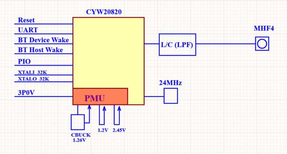
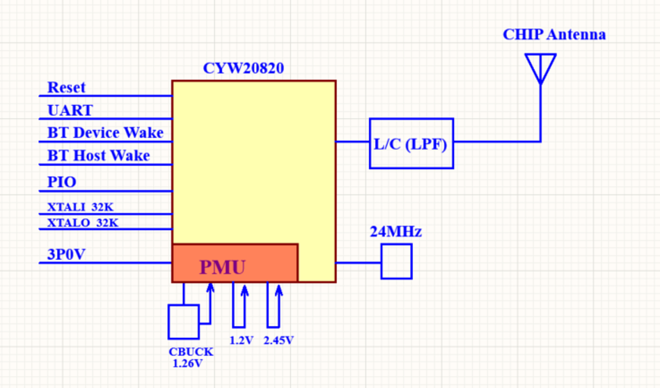
Pin-Out / Package Layout
MHF4 Connector Variant Footprint and Pin Definitions
Note: The following footprint and pin definitions apply to the Vela IF820. There are two module footprints, depending on which variant of the module is used. It is important to ensure you are using the correct version on your design.
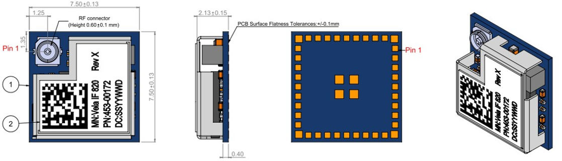
MHF4 Connector Variant Mechanical Definition
Module dimensions of MHF4 connector variant module is 7.5 x 7.5 x 2.15 mm.
MHF4 Connector Variant Module Footprint
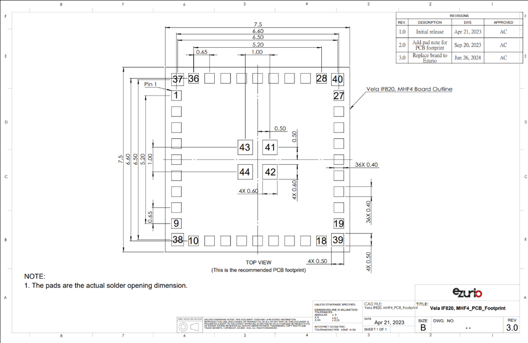
MHF4 Connector Variant Module Pin Definition
| Pin # | Name | EZ-Serial FW Default Function | Pin When Not Used | I/O | Voltage Ref. | Description |
|---|---|---|---|---|---|---|
| 1 | BT_DEV_WAKE | NA | floating | I | VDDIO | A signal from the host to the CYW20820 indicating that the host requires attention. |
| 2 | BT_HOST_WAKE | BT_HOST_WAKE | floating | O | VDDIO | A signal from the CYW20820 device to the host indicating that the Bluetooth® device requires attention. Note: this pin is an output from the IF820; with EZ-Serial it is used for low-power operation and is high when the module is awake and ready to accept commands, otherwise low. |
| 3 | GND | - | - | NA | ||
| 4 | P28 | I2C CLK | floating | I/O | VDDIO | Recommended functions for P28: PWM2; SCL3 (master and slave); Optical control output: QOC2; A/D converter input 11; Current: 16 mA sink. P28 can also be remapped using Supermux I/O functions as defined in the Supermux I/O Function Defined Table. |
| 5 | P4 | GPIO for USER LED | floating | I/O | VDDIO | Recommended functions for P4: Keyboard scan input (row): KSI4; Quadrature: QDY0; SPI_1: MOSI (master only). P4 can also be remapped using Supermux I/O functions as defined in the Supermux I/O Function Defined Table. |
| 6 | P2 | SWDCLK | floating | I/O | VDDIO | Recommended functions for P2: Keyboard scan input (row): KSI2; Quadrature: QDX0; SPI_1: MOSI (master only); UART1_RTS_N. P2 can also be remapped using Supermux I/O functions as defined in the Supermux I/O Function Defined Table. |
| 7 | P15 | SPI_CS | floating | I/O | VDDIO | Recommended functions for P15: Keyboard scan output (column): KSO7; A/D converter input 20. P15 can also be remapped using Supermux I/O functions as defined in the Supermux I/O Function Defined Table. |
| 8 | P5 | GPIO for Hardware Interrupt | floating | I/O | VDDIO | Recommended functions for P5: Keyboard scan input (row): KSI5; Quadrature: QDY1; Peripheral UART: puart_tx; SPI_1: MISO (slave only); I2C: SDA. P5 can also be remapped using Supermux I/O functions as defined in the Supermux I/O Function Defined Table. |
| 9 | P8 | GPIO for Analog | floating | I/O | VDDIO | Recommended functions for P8: Keyboard scan output (column): KSO0; A/D converter input 27; External T/R switch control: ~tx_pd. P8 can also be remapped using Supermux I/O functions as defined in the Supermux I/O Function Defined Table. |
| 10 | VDDIO | I | VDDIO | 1.71V to 3.3V is recommended to supply for digital I/O | ||
| 11 | GND | - | - | NA | ||
| 12 | XTALI_32K | XTALI_32K | floating | I | VDDIO | Low-power oscillator input. Highly recommend placing external 32.768 kHz crystal. Using the external crystal guarantees the lowest power and highest timing accuracy. |
| 13 | XTALO_32K | XTALO_32K | floating | O | VDDIO | Low-power oscillator output. Highly recommend placing external 32.768 kHz crystal. Using the external crystal guarantees the lowest power and highest timing accuracy. |
| 14 | P3 | SWDIO | floating | I/O | VDDIO | Recommended functions for P3: Keyboard scan input (row): KSI3; Quadrature: QDX1; UART1_CTS_N; SPI_1: SPI_CLK (master only). P3 can also be remapped using Supermux I/O functions as defined in the Supermux I/O Function Defined Table. |
| 15 | P6 | SPI_SCK | floating | I/O | VDDIO | Recommended functions for P6: Keyboard scan input (row): KSI6; Quadrature: QDZ0; Peripheral UART: puart_rts; PWM2. P6 can also be remapped using Supermux I/O functions as defined in the Supermux I/O Function Defined Table. |
| 16 | P17 | SPI_MISO | floating | I/O | VDDIO | Recommended functions for P17: Keyboard scan output (column): KSO9; A/D converter input 18. P17 can also be remapped using Supermux I/O functions as defined in the Supermux I/O Function Defined Table. |
| 17 | P9 | SPI_MOSI | floating | I/O | VDDIO | Recommended functions for P9: Keyboard scan output (column): KSO1; A/D converter input 26; External T/R switch control: tx_pd. P9 can also be remapped using Supermux I/O functions as defined in the Supermux I/O Function Defined Table. |
| 18 | P12 | LP_MODE | floating | I/O | VDDIO | Recommended functions for P12: Keyboard scan output (column): KSO4; A/D converter input 23. P12 can also be remapped using Supermux I/O functions as defined in the Supermux I/O Function Defined Table. |
| 19 | P13 | CYSPP/SPP | floating | I/O | VDDIO | Recommended functions for P13: Keyboard scan output (column): KSO5; A/D converter input 22; PWM3. P13 can also be remapped using Supermux I/O functions as defined in the Supermux I/O Function Defined Table. |
| 20 | P1 | CP_ROLE | floating | I/O | VDDIO | Recommended functions for P1: Keyboard scan input (row): KSI1; A/D converter input 28; Peripheral UART: puart_rts; SPI_1: MISO (slave only); UART1_RXD. Can also be remapped using Supermux I/O functions as defined in the Supermux I/O Function Defined Table. |
| 21 | P11 | P_UART_RTS (optional) | floating | I/O | VDDIO | Recommended functions for P11: Keyboard scan output (column): KSO3; A/D converter input 24. P11 can also be remapped using Supermux I/O functions as defined in the Supermux I/O Function Defined Table. |
| 22 | P10 | P_UART_CTS (optional) | floating | I/O | VDDIO | Recommended functions for P10: Keyboard scan output (column): KSO2; A/D converter input 25; External PA ramp control: PA_Ramp. P10 can also be remapped using Supermux I/O functions as defined in the Supermux I/O Function Defined Table. |
| 23 | P27 | Connection Indication GPIO | floating | I/O | VDDIO | Recommended functions for P27: Keyboard scan output (column): KSO19; PWM1; SPI_1: MOSI (master only); Optical control output: QOC1; Current: 16 mA sink. P27 can also be remapped using Supermux I/O functions as defined in the Supermux I/O Function Defined Table. |
| 24 | RST | RST_L | floating | I | VDDIO | Active-low system reset with internal pull-up resistor. NOTE — Required for flashing EZ-Serial and HCI firmware. |
| 25 | P0 | GPIO for user button | floating | I/O | VDDIO | Recommended functions for P0: Keyboard scan input (row): KSI0; A/D converter input 29; Peripheral UART: puart_tx; SPI_1: MOSI (master only); UART1_TXD. P0 can also be remapped using Supermux I/O functions as defined in the Supermux I/O Function Defined Table. |
| 26 | P37 | P_UART_RXD (REQUIRED) | floating | I/O | VDDIO | Recommended functions for P37: A/D converter input 2; Quadrature: QDZ1; SPI_1: MISO (slave only); Auxiliary clock output: ACLK1; I2C: SCL. P37 can also be remapped using Supermux I/O functions as defined in the Supermux I/O Function Defined Table. |
| 27 | P32 | P_UART_TXD (REQUIRED) | floating | I/O | VDDIO | Recommended functions P32: A/D converter input 7; Quadrature: QDX0; Auxiliary clock output: ACLK0; Peripheral UART: puart_tx. P32 can also be remapped using Supermux I/O functions as defined in the Supermux I/O Function Defined Table. |
| 28 | P14 | GPIO for peripheral RST_L | floating | I/O | VDDIO | Recommended functions for P14: Keyboard scan output (column): KSO6; A/D converter input 21; PWM2. P14 can also be remapped using Supermux I/O functions as defined in the Supermux I/O Function Defined Table. |
| 29 | P29 | I2C DATA | floating | I/O | VDDIO | Recommended functions for P29: PWM3; SDA3 (master and slave); Optical control output: QOC3; A/D converter input 10; Current: 16 mA sink. P29 can also be remapped using Supermux I/O functions as defined in the Supermux I/O Function Defined Table. |
| 30 | P26 | GPIO for PWM | floating | I/O | VDDIO | Recommended functions for P26: Keyboard scan output (column): KSO18; PWM0; SPI_1: SPI_CS (slave only); Optical control output: QOC0; Current: 16 mA sink. P26 can also be remapped using Supermux I/O functions as defined in the Supermux I/O Function Defined Table. |
| 31 | 3P0V | I | 3V | Power supply input | ||
| 32 | GND | - | - | Ground | ||
| 33 | BT_UART_RTS | HCI_UART_RTS (Required) | O, PU | VDDIO | Request to send (RTS) for HCI UART interface. NOTE — Required for flashing EZ-Serial and HCI firmware. | |
| 34 | BT_UART_TXD | HCI_UART_TXD (Required) | O, PU | VDDIO | UART serial output. Serial data output for the HCI UART interface. NOTE — Required for flashing EZ-Serial and HCI firmware. | |
| 35 | BT_UART_RXD | HCI_UART_RXD (Required) | I | VDDIO | UART serial input. Serial data input for the HCI UART interface. NOTE — Required for flashing EZ-Serial and HCI firmware. | |
| 36 | BT_UART_CTS | HCI_UART_CTS (Required) | I, PU | VDDIO | Clear to send (CTS) for HCI UART interface. NOTE — Required for flashing EZ-Serial and HCI firmware. | |
| 37–44 | GND | - | - | Ground |
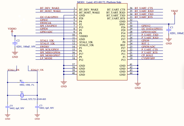
Reference Schematic Design (MHF4 Variant)
Note: It is recommended to put a 100nF bypass capacitor in the 3P0V (pin 31) and VDDIO (pin 10). Highly recommend placing external 32.768 kHz crystal. Using the external crystal guarantees the lowest power and highest timing accuracy. BT_UART signals (x4) are required for flashing EZ-Serial and HCI firmware.
Supermux I/O Function Defined Table
| Input | ||
|---|---|---|
| SWDCK | SPI2_CS | SCL2 |
| SWDIO | SPI2_MOSI | SDA2 |
| SPI1_CLK | SPI2_MISO | PCM_IN |
| SPI1_CS | SPI2_IO2 | PCM_CLK |
| SPI1_MOSI | SPI2_IO3 | PCM_SYNC |
| SPI1_MISO | SPI2_INT | I2S_DI |
| SPI1_IO2 | puart_rx | I2S_WS |
| SPI1_IO3 | puart_cts_n | I2S_CLK |
| SPI1_INT | SCL | PDM_IN_Ch_1 |
| SPI2_CLK | SDA | PDM_IN_Ch 2 |
| Output | |||
|---|---|---|---|
| do_P# (data out of GPIO. For example: P0) | kso4 | kso19 | SCL2 |
| do_PCM_IN | kso5 | do_P# pwm0 | puart_tx (uart2_tx) |
| do_PCM_OUT | kso6 | do_P# pwm1 | puart_rts_n (uart2_rts_n) |
| do_PCM_CLK | kso7 | do_P# pwm2 | SPI1_CLK |
| do_PCM_SYNC | kso8 | do_P# pwm3 | SPI1_CS |
| do_I2S_DO | kso9 | do_P# pwm4 | SPI1_MOSI |
| do_I2S_DI | kso10 | do_P# pwm5 | SPI1_MISO |
| do_I2S_WS | kso11 | aclk0 | SPI1_IO2 |
| do_I2S_CLK | kso12 | aclk1 | SPI1_IO3 |
| do_CLK_REQ | kso13 | HID_OFF | SPI2_CLK |
| IR_TX | kso14 | pa_ramp | SPI2_CS |
| kso0 | kso15 | tx_pd | SPI2_MOSI |
| kso1 | kso16 | ~tx_pd | SPI2_MISO |
| kso2 | kso17 | SWDIO | SPI2_IO2 |
| kso3 | kso18 | SDA2 | SPI2_IO3 |
Integrated Antenna Variant Footprint and Pin Definitions
Integrated Antenna Variant Mechanical Definition
Module dimensions of integrated antenna variant module is 12.5 x 9.3 x 2.15 mm.
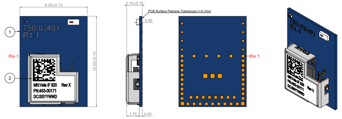
Integrated Antenna Variant Module Footprint
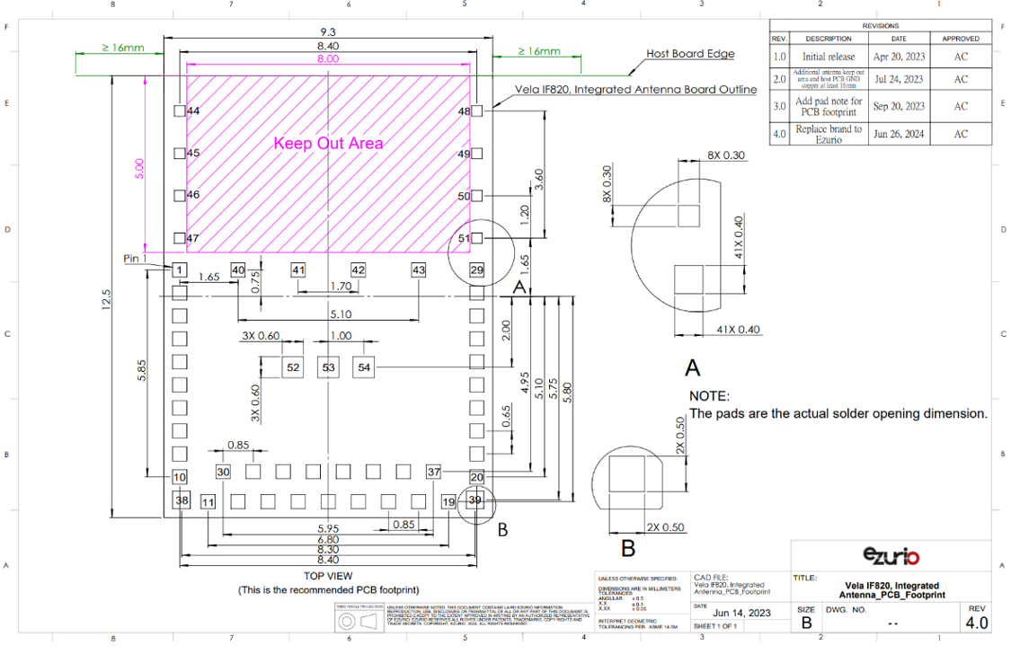
Integrated Antenna Variant Module Pin Definition
| Pin # | Name | EZ-Serial FW Default Function | Pin When Not Used | I/O | Voltage Ref. | Description |
|---|---|---|---|---|---|---|
| 1 | GND | - | - | Ground | ||
| 2 | VDDIO | I | VDDIO | 1.71V to 3.3V is recommended to supply for digital I/O | ||
| 3 | GND | - | - | Ground | ||
| 4 | XTALI_32K | XTALI_32K | floating | I | VDDIO | Low-power oscillator input. Highly recommend to implement 32.768 kHz crystal; if not, link issues may occur. |
| 5 | XTALO_32K | XTALO_32K | floating | O | VDDIO | Low-power oscillator output. Highly recommend to implement 32.768 kHz crystal; if not, link issues may occur. |
| 6 | P15 | SPI_CS | floating | I/O | VDDIO | Recommended functions for P15: Keyboard scan output (column): KSO7; A/D converter input 20. P15 can also be remapped using Supermux I/O functions as defined in the Supermux I/O Function Defined Table. |
| 7 | P8 | GPIO for Analog | floating | I/O | VDDIO | Recommended functions for P8: Keyboard scan output (column): KSO0; A/D converter input 27; External T/R switch control: ~tx_pd. P8 can also be remapped using Supermux I/O functions as defined in the Supermux I/O Function Defined Table. |
| 8 | P2 | SWDCLK | floating | I/O | VDDIO | Recommended functions for P2: Keyboard scan input (row): KSI2; Quadrature: QDX0; SPI_1: MOSI (master only); UART1_RTS_N. P2 can also be remapped using Supermux I/O functions as defined in the Supermux I/O Function Defined Table. |
| 9 | P3 | SWDIO | floating | I/O | VDDIO | Recommended functions for P3: Keyboard scan input (row): KSI3; Quadrature: QDX1; UART1_CTS_N; SPI_1: SPI_CLK (master only). P3 can also be remapped using Supermux I/O functions as defined in the Supermux I/O Function Defined Table. |
| 10 | P6 | SPI_SCK | floating | I/O | VDDIO | Recommended functions for P6: Keyboard scan input (row): KSI6; Quadrature: QDZ0; Peripheral UART: puart_rts; PWM2. P6 can also be remapped using Supermux I/O functions as defined in the Supermux I/O Function Defined Table. |
| 11 | P17 | SPI_MISO | floating | I/O | VDDIO | Recommended functions for P17: Keyboard scan output (column): KSO9; A/D converter input 18. P17 can also be remapped using Supermux I/O functions as defined in the Supermux I/O Function Defined Table. |
| 12 | P13 | CYSPP/SPP | floating | I/O | VDDIO | CYSPP Input/output CYSPP mode control. Assert (LOW) for CYSPP data mode, de-assert (HIGH) for command mode. Recommended functions for P13: KSO5; A/D converter input 22; PWM3. P13 can also be remapped using Supermux I/O functions as defined in the Supermux I/O Function Defined Table. |
| 13 | P9 | SPI_MOSI | floating | I/O | VDDIO | Recommended functions for P9: KSO1; A/D converter input 26; External T/R switch control: tx_pd. P9 can also be remapped using Supermux I/O functions as defined in the Supermux I/O Function Defined Table. |
| 14 | P10 | P_UART_CTS (optional) | floating | I/O | VDDIO | Recommended functions for P10: KSO2; A/D converter input 25; External PA ramp control: PA_Ramp. P10 can also be remapped using Supermux I/O functions as defined in the Supermux I/O Function Defined Table. |
| 15 | P37 | P_UART_RXD (REQUIRED) | floating | I/O | VDDIO | Recommended functions for P37: A/D converter input 2; QDZ1; SPI_1: MISO (slave only); ACLK1; I2C: SCL. P37 can also be remapped using Supermux I/O functions as defined in the Supermux I/O Function Defined Table. |
| 16 | P11 | P_UART_RTS (optional) | floating | I/O | VDDIO | Recommended functions for P11: KSO3; A/D converter input 24. P11 can also be remapped using Supermux I/O functions as defined in the Supermux I/O Function Defined Table. |
| 17 | P32 | P_UART_TXD (REQUIRED) | floating | I/O | VDDIO | Recommended functions P32: A/D converter input 7; QDX0; ACLK0; Peripheral UART: puart_tx. P32 can also be remapped using Supermux I/O functions as defined in the Supermux I/O Function Defined Table. |
| 18 | P14 | GPIO for peripheral RST_L | floating | I/O | VDDIO | Recommended functions for P14: KSO6; A/D converter input 21; PWM2. P14 can also be remapped using Supermux I/O functions as defined in the Supermux I/O Function Defined Table. |
| 19 | P5 | GPIO for Hardware Interrupt | floating | I/O | VDDIO | Recommended functions for P5: KSI5; QDY1; Peripheral UART: puart_tx; SPI_1: MISO (slave only); I2C: SDA. P5 can also be remapped using Supermux I/O functions as defined in the Supermux I/O Function Defined Table. |
| 20 | P28 | I2C_CLK | floating | I/O | VDDIO | Recommended functions for P28: PWM2; SCL3 (master and slave); QOC2; A/D converter input 11; Current: 16 mA sink. P28 can also be remapped using Supermux I/O functions as defined in the Supermux I/O Function Defined Table. |
| 21 | GND | - | - | Ground | ||
| 22 | 3P0V | I | 3V | Power supply input | ||
| 23 | GND | - | - | Ground | ||
| 24 | BT_UART_RTS | HCI_UART_RTS (Required) | floating | O, PU | VDDIO | Request to send (RTS) for HCI UART interface. NOTE — Required for flashing EZ-Serial and HCI firmware. |
| 25 | BT_UART_TXD | HCI_UART_TXD (Required) | floating | O, PU | VDDIO | UART serial output. Serial data output for the HCI UART interface. NOTE — Required for flashing EZ-Serial and HCI firmware. |
| 26 | BT_UART_RXD | HCI_UART_RXD (Required) | floating | I | VDDIO | UART serial input. Serial data input for the HCI UART interface. NOTE — Required for flashing EZ-Serial and HCI firmware. |
| 27 | BT_UART_CTS | HCI_UART_CTS (Required) | floating | I, PU | VDDIO | Clear to send (CTS) for HCI UART interface. NOTE — Required for flashing EZ-Serial and HCI firmware. |
| 28 | BT_DEV_WAKE | NA | floating | I | VDDIO | A signal from the host to the CYW20820 indicating that the host requires attention. |
| 29 | BT_HOST_WAKE | BT_HOST_WAKE | floating | O | VDDIO | A signal from the CYW20820 device to the host indicating that the Bluetooth® device requires attention. Note: this pin is an output from the IF820; with EZ-Serial it is used for low-power operation and is high when the module is awake and ready to accept commands, otherwise low. |
| 30 | P12 | LP_MODE | floating | I/O | VDDIO | Recommended functions for P12: KSO4; A/D converter input 23. P12 can also be remapped using Supermux I/O functions as defined in the Supermux I/O Function Defined Table. |
| 31 | P1 | CP_ROLE | floating | I/O | VDDIO | Recommended functions for P1: KSI1; A/D converter input 28; Peripheral UART: puart_rts; SPI_1: MISO (slave only); UART1_RXD. Can also be remapped using Supermux I/O functions as defined in the Supermux I/O Function Defined Table. |
| 32 | P0 | GPIO for user button | floating | I/O | VDDIO | Recommended functions for P0: KSI0; A/D converter input 29; Peripheral UART: puart_tx; SPI_1: MOSI (master only); UART1_TXD. P0 can also be remapped using Supermux I/O functions as defined in the Supermux I/O Function Defined Table. |
| 33 | P27 | Connection Indication GPIO | floating | I/O | VDDIO | Recommended functions for P27: KSO19; PWM1; SPI_1: MOSI (master only); QOC1; Current: 16 mA sink. P27 can also be remapped using Supermux I/O functions as defined in the Supermux I/O Function Defined Table. |
| 34 | RST | RST_L | floating | I | VDDIO | Active-low system reset with internal pull-up resistor. NOTE — Required for flashing EZ-Serial and HCI firmware. |
| 35 | P29 | I2C_DATA | floating | I/O | VDDIO | Recommended functions for P29: PWM3; SDA3 (master and slave); QOC3; A/D converter input 10; Current: 16 mA sink. P29 can also be remapped using Supermux I/O functions as defined in the Supermux I/O Function Defined Table. |
| 36 | P26 | GPIO for PWM | floating | I/O | VDDIO | Recommended functions for P26: KSO18; PWM0; SPI_1: SPI_CS (slave only); QOC0; Current: 16 mA sink. P26 can also be remapped using Supermux I/O functions as defined in the Supermux I/O Function Defined Table. |
| 37 | P4 | GPIO for USER LED | floating | I/O | VDDIO | Recommended functions for P4: KSI4; QDY0; SPI_1: MOSI (master only). P4 can also be remapped using Supermux I/O functions as defined in the Supermux I/O Function Defined Table. |
| 38–54 | GND | - | - | Ground |
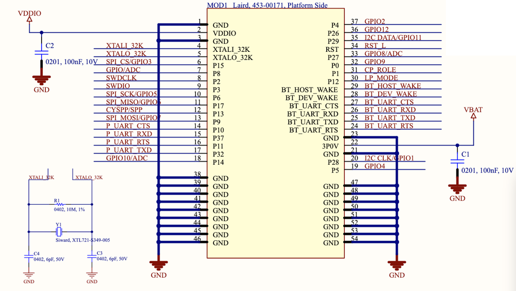
Reference Schematic Design (Integrated Antenna Variant)
Note: It is recommended to put bypass capacitors 100nF in the 3P0V (pin 22) and VDDIO (pin 2). Highly recommend to implement 32.768 kHz crystal (pin 4, pin 5). Using the external crystal guarantees the lowest power and highest timing accuracy. BT_UART signals (x4) are required for flashing EZ-Serial and HCI firmware.
Mechanical Drawings
See pin definition sections above for mechanical details per variant. Images referenced above (Figures 9, 12) include detailed mechanical drawings.
Host Interface Specifications
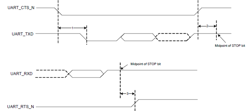
High-Speed UART Specifications
| Reference | Characteristics | Min | Typ | Max | Units |
|---|---|---|---|---|---|
| 1 | Delay time, UART_CTS_N LOW to UART_TXD valid. | — | — | 1.5 | Bit periods |
| 2 | Setup time, UART_CTS_N HIGH before midpoint of stop bit. | — | 0.67 | ||
| 3 | Delay time, midpoint of stop bit to UART_RTS_N HIGH. | — | — | 1.33 |
SPI Timing
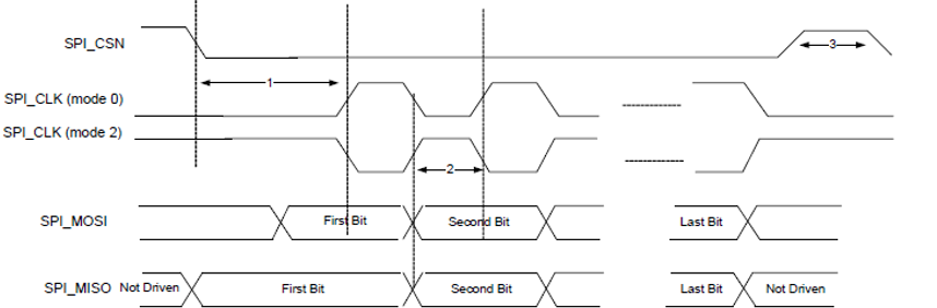
SPI mode 0 and 2
| Reference | Characteristics | Min | Max | Units |
|---|---|---|---|---|
| 1 | Time from master assert SPI_CSN to first clock edge | 45 | — | ns |
| 2 | Setup time for MOSI data lines | 6 | 1/2 SCK | |
| 3 | Idle time between subsequent SPI transactions | 1 SCK | — |
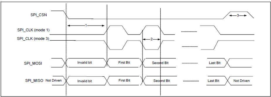
SPI mode 1 and 3
| Reference | Characteristics | Min | Max | Units |
|---|---|---|---|---|
| 1 | Time from master assert SPI_CSN to first clock edge | 45 | — | ns |
| 2 | Setup time for MOSI data lines | 6 | 1/2 SCK | |
| 3 | Idle time between subsequent SPI transactions | 1 SCK | — |
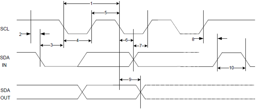
I2C Timing
| Reference | Characteristics | Min | Max | Units |
|---|---|---|---|---|
| 1 | Clock frequency | — | 100 / 400 / 800 / 1000 | KHz |
| 2 | START condition setup time | 650 | — | us |
| 3 | START condition hold time | 280 | — | |
| 4 | Clock low time | 650 | — | |
| 5 | Clock high time | 280 | ||
| 6 | Data input hold time [1] | 0 | — | |
| 7 | Data input setup time | 100 | — | |
| 8 | STOP condition setup time | 280 | ||
| 9 | Output valid from clock | — | 400 | |
| 10 | Bus free time [2] | 650 | — |
Notes:
- As a transmitter, 125 ns of delay is provided to bridge the undefined region of the falling edge of SCL to avoid unintended generation of START or STOP conditions.
- Time that the CBUS must be free before a new transaction can start.
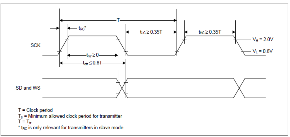
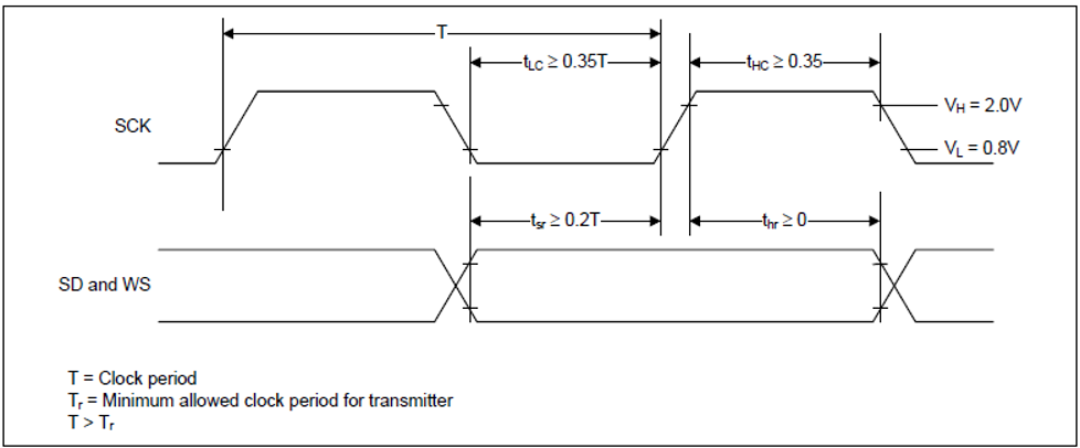
I2S Timing
| Parameter | Transmitter Lower Min | Transmitter Lower Max | Transmitter Upper Min | Transmitter Upper Max | Receiver Lower Min | Receiver Lower Max | Receiver Upper Min | Receiver Upper Max | Notes |
|---|---|---|---|---|---|---|---|---|---|
| Clock Period T | Ttr | - | - | - | Tr | - | - | - | [3] |
| Master mode HIGH tHC | 0.35 x Ttr | - | - | - | 0.35 x Ttr | - | - | - | [4] |
| Master mode LOW tLC | 0.35 x Ttr | - | - | - | 0.35 x Ttr | - | - | - | [4] |
| Slave mode HIGH tHC | - | 0.35 x Ttr | - | - | - | 0.35 x Ttr | - | - | [3] |
| Slave mode LOW tLC | - | 0.35 x Ttr | - | - | - | 0.35 x Ttr | - | - | [3] |
| Rise time tRC | - | - | 0.15 x Ttr | - | - | - | - | - | [4] |
| Transmitter Delay tdtr | - | - | - | 0.8 x T | - | - | - | - | [5] |
| Hold time thtr | 0 | - | - | - | - | - | - | - | [4] |
| Receiver Setup time tsr | - | - | - | - | 0.2 x Ttr | - | - | - | [6] |
| Hold time thr | - | - | - | - | 0.2 x Ttr | - | - | - | [6] |
Notes:
- The system clock period T must be greater than Ttr and Tr because both the transmitter and receiver must be able to handle the data transfer rate.
- At all data rates in master mode, the transmitter or receiver generates a clock signal with a fixed mark/space ratio. For this reason, tHC and tLC are specified with respect to T.
- In slave mode, the transmitter and receiver need a clock signal with minimum HIGH and LOW periods so that they can detect the signal. So long as the minimum periods are greater than 0.35Tr, any clock that meets the requirements can be used.
- Because the delay (tdtr) and the maximum transmitter speed (defined by Ttr) are related, a fast transmitter driven by a slow clock edge can result in tdtr not exceeding tRC which means thtr becomes zero or negative. Therefore, the transmitter must guarantee that thtr is greater than or equal to zero, so long as the clock rise-time tRC is not more than tRCmax, where tRCmax is not less than 0.15Ttr.
Electrical Characteristics
Absolute Maximum Ratings
Table 4 summarizes the absolute maximum ratings and Table 5 lists the recommended operating conditions for the Vela IF820 series wireless module. Absolute maximum ratings are those values beyond which damage to the device can occur. Operating this device outside of the listed maximum ratings and operating conditions may damage the device and void the warranty.
Note: Maximum rating for signals follows the supply domain of the signals.
| Symbol | Parameter | Minimum | Typical | Maximum | Unit |
|---|---|---|---|---|---|
| 3P0V | Power supply for Internal Regulators | -0.5 | 3.45 | V | |
| VDDIO | DC supply voltage for digital I/O | -0.5 | 3.45 | V |
Recommended Operating Conditions
| Symbol (Domain) | Parameter | Min | Typ | Max | Unit |
|---|---|---|---|---|---|
| 3P0V | Power supply for Internal Regulators | 2.6 | 3.0 | 3.3 | V |
| VDDIO | DC supply voltage for digital I/O | 1.71 | 1.8/3.0 | 3.3 | V |
| T-ambient | Ambient temperature | -40 | 25 | 85 | °C |
DC Electrical Characteristics
The following lists the general DC electrical characteristics over recommended operating conditions (unless otherwise specified).
| Symbol | Parameter | Min | Typ | Max | Unit |
|---|---|---|---|---|---|
| VIL | Input low voltage (VDDIO = 3V) | — | — | 0.8 | V |
| VIH | Input high voltage (VDDIO = 3V) | 2.4 | — | — | |
| VIL | Input low voltage (VDDIO = 1.8V) | — | — | 0.4 | |
| VIH | Input high voltage (VDDIO = 1.8V) | 1.4 | — | — | |
| VOL | Output low voltage | — | — | 0.4 | |
| VOH | Output high voltage | VDDIO - 0.4V | — | — | |
| IIL | Input low current | — | — | 1 | uA |
| IIH | Input high current | — | — | 1 | |
| IOL | Output low current (VDDIO = 3V, VOL = 0.4V) | — | — | 4 | mA |
| IOL | Output low current (VDDIO = 3V, VOL = 1.8V) | — | — | 2 | |
| IOH | Output high current (VDDIO = 3V, VOH = 2.6V) | — | — | 8 | |
| IOH | Output high current (VDDIO = 1.8V, VOH = 1.4V) | — | — | 4 | |
| CIN | Input capacitance | — | — | 0.4 | pF |
General Current Consumption
See Bluetooth Current Consumption for current consumption values by operating mode.
Signal Levels and Interface Specs
See Host Interface Specifications for UART, SPI, I2C, and I2S signal level specifications.
Radio Characteristics
Bluetooth Receiver Characteristics
Basic Rate (BR) receiver performance (3V)
| Test Parameter | Min | Typ | Max | Bluetooth Spec. | Unit |
|---|---|---|---|---|---|
| Sensitivity (1DH5) BER ≤ 0.1% | — | -90 | -87 | ≤ -70 | dBm |
| Maximum Input BER ≤ 0.1% | — | — | -20 | ≥ -20 | dBm |
Enhanced Data Rate (EDR) receiver performance (3V)
| Test Parameter | Min | Typ | Max | Bluetooth Spec. | Unit |
|---|---|---|---|---|---|
| Sensitivity (BER ≤ 0.01%) π/4-DQPSK | — | -92.5 | -89.5 | ≤ -70 | dBm |
| Sensitivity (BER ≤ 0.01%) 8-DPSK | — | -86 | -83 | ≤ -70 | dBm |
Bluetooth LE RF Specifications (3V)
| Parameter | Conditions | Min | Typ | Max | Unit |
|---|---|---|---|---|---|
| Frequency range | — | 2402 | — | 2480 | MHz |
| Rx sensitivity | GFSK, 30.8% PER, 1 Mbps | — | -94 | -91 | dBm |
| Rx sensitivity | GFSK, 30.8% PER, 2 Mbps | — | -90 | -87 | dBm |
Note: Dirty TX is Off.
Bluetooth Transmitter Characteristics
Basic Rate (BR) transmitter performance at 25°C (3V)
| Test Parameter | Min | Typ | Max | Bluetooth Spec. | Unit |
|---|---|---|---|---|---|
| RF Output Power (test at MHF4 connector) — BR | — | 6 | 7.5 | 0 ~ +20 | dBm |
| RF Output Power (test at MHF4 connector) — EDR 2M | — | 1.5 | 2.5 | dBm | |
| RF Output Power (test at MHF4 connector) — EDR 3M | — | 0.5 | 1.5 | dBm | |
| Max EIRP (Integrated antenna variant) | 10 | dBm | |||
| Frequency Range | 2.4 | — | 2.480 | 2.4 ≤ f ≤ 2.480 | GHz |
Bluetooth LE TX Power
| Parameter | Conditions | Min | Typ | Max | Unit |
|---|---|---|---|---|---|
| RF Output Power (test at MHF4 connector) — 1M | — | 6 | 7.5 | dBm | |
| RF Output Power (test at MHF4 connector) — 2M | — | 6 | 7.5 | dBm | |
| Max EIRP (Integrated antenna variant) | 10 | dBm |
Note: The Bluetooth LE TX power cannot exceed 10 dBm EIRP specification limit. The front-end losses and antenna gain/loss must be factored in so as not to exceed the limit.
Bluetooth Current Consumption
Bluetooth current consumption, VBAT=3V VDDIO=3V, MHF4 connector variant
| Operating Mode | Data Rate | Module 3V (mA) |
|---|---|---|
| TX | DH1 | 13.5 |
| TX | DH3 | 13.5 |
| TX | DH5 | 13.5 |
| TX | 2DH1 | 20.2 |
| TX | 2DH3 | 20 |
| TX | 2DH5 | 20.1 |
| TX | 3DH1 | 19.8 |
| TX | 3DH3 | 20 |
| TX | 3DH5 | 20.1 |
| TX | LE1M | 13.3 |
| TX | LE2M | 13.3 |
| RX | DH5 | 6.2 |
| RX | LE1M | 6.4 |
| RX | LE2M | 7.4 |
Bluetooth current consumption, VBAT=3V VDDIO=3V, Integrated antenna variant
| Operating Mode | Data Rate | Module 3V (mA) |
|---|---|---|
| TX | DH1 | 14.4 |
| TX | DH3 | 14.5 |
| TX | DH5 | 14.5 |
| TX | 2DH1 | 19.9 |
| TX | 2DH3 | 20.4 |
| TX | 2DH5 | 20.4 |
| TX | 3DH1 | 20.2 |
| TX | 3DH3 | 20.1 |
| TX | 3DH5 | 20.1 |
| TX | LE1M | 16.4 |
| TX | LE2M | 16.3 |
| RX | DH5 | 6.2 |
| RX | LE1M | 6.4 |
| RX | LE2M | 7.4 |
Note: Current consumption is measured at average of the TX-on time.
Power Management & Consumption
Power Consumption
See Bluetooth Current Consumption for typical current consumption values by operating mode.
Integration Guidelines
Antenna Characteristics
453-00171 Integrated Chip Antenna Performance
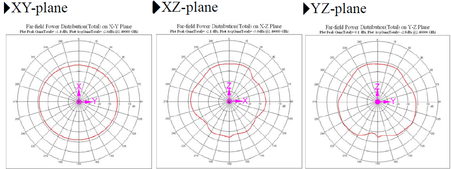
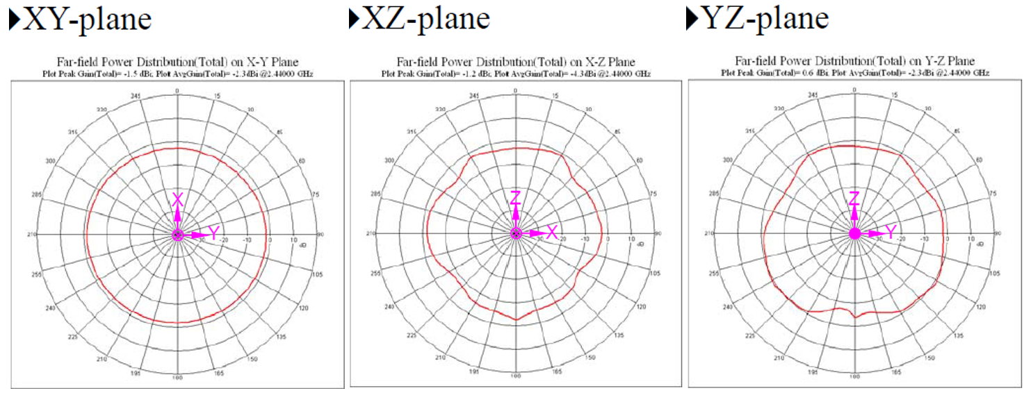
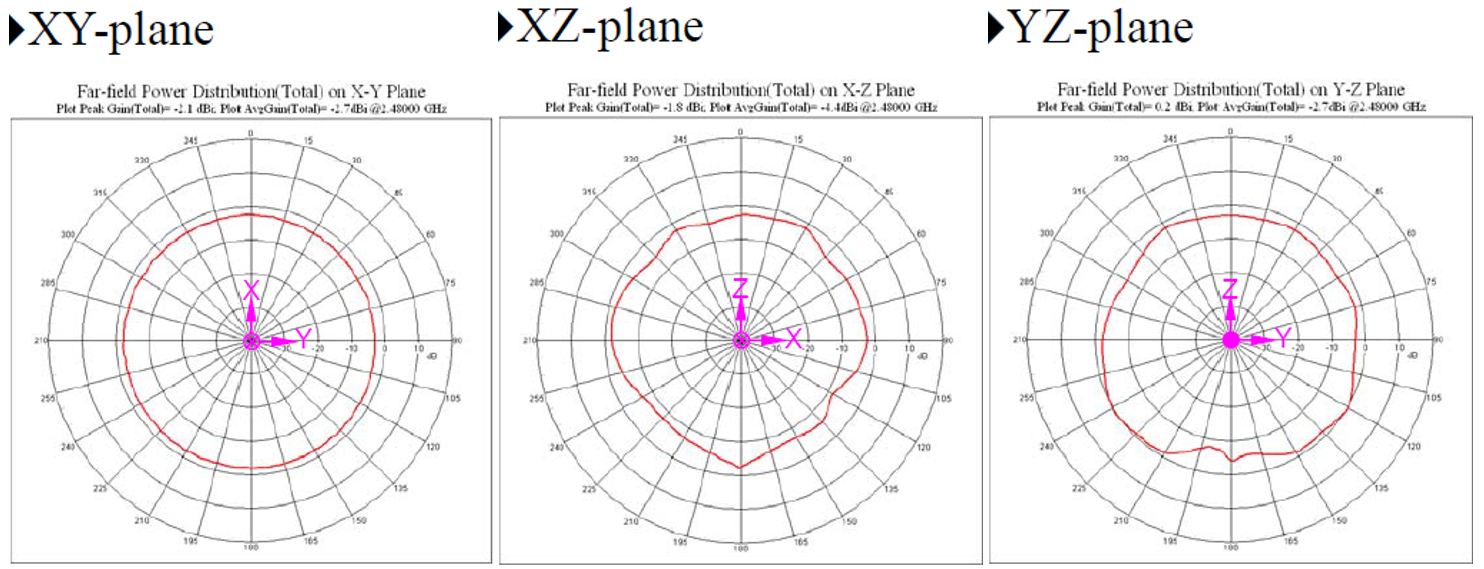
The following are details and plots of the measured radiation performance of the chip antenna on the Vela IF820 module with integrated antenna (part numbers 453-00171R and 453-00171C).
Summary of Antenna Performance
| Unit in dBi | XY-plane Peak | XY-plane Avg. | XZ-plane Peak | XZ-plane Avg. | YZ-plane Peak | YZ-plane Avg. | Efficiency |
|---|---|---|---|---|---|---|---|
| @2400MHz | -1.4 | -2.6 | -2.1 | -5 | 0.1 | -2.8 | 45% |
| @2440MHz | -1.5 | -2.3 | -1.2 | -4.3 | 0.6 | -2.3 | 51% |
| @2480MHz | -2.1 | -2.7 | -1.8 | -4.4 | 0.2 | -2.7 | 48% |
Note: The result is measured with Ezurio DVK part # 453-00171-K1.
453-00185 USB Adapter Integrated Antenna Performance
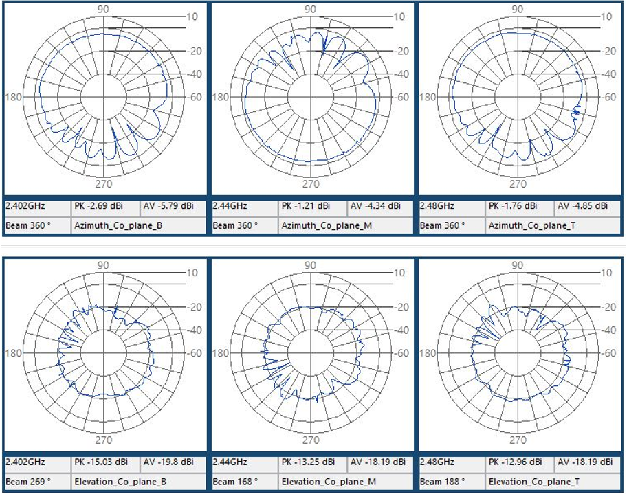
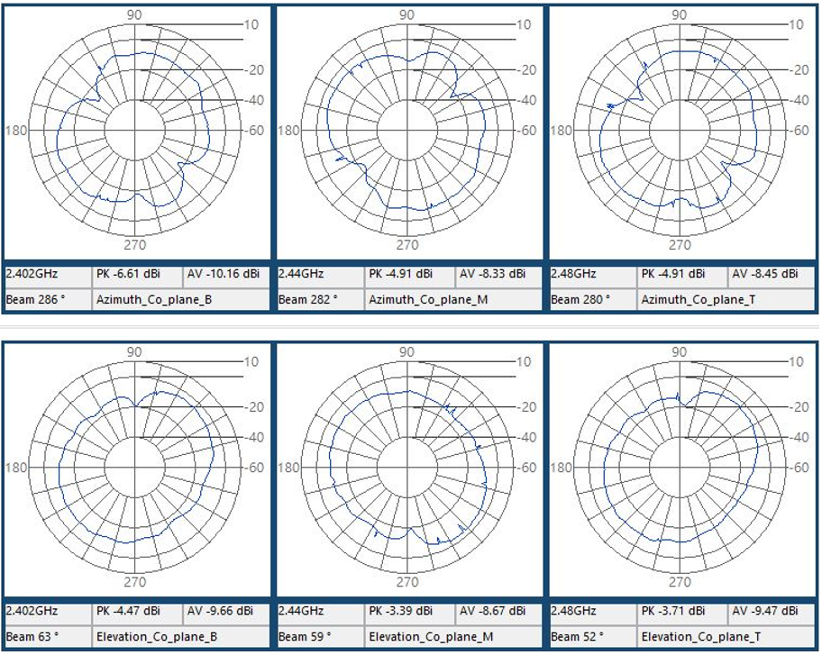
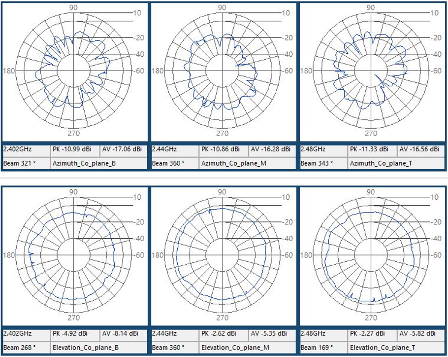
The following are details and plots of the measured radiation performance of the integrated antenna on the Vela IF820 USB adapter (part number 453-00185).
Summary of Antenna Performance
| Unit in dBi | XY-plane Peak | XY-plane Avg. | XZ-plane Peak | XZ-plane Avg. | YZ-plane Peak | YZ-plane Avg. |
|---|---|---|---|---|---|---|
| @2400MHz | -2.69 | -5.79 | -4.47 | -9.66 | -4.92 | -8.14 |
| @2440MHz | -1.21 | -4.34 | -3.39 | -8.67 | -2.62 | -5.35 |
| @2480MHz | -1.76 | -4.85 | -3.71 | -9.47 | -2.27 | -5.82 |
Note: The result is measured with USB adapter (part # 450-00185).
Circuit (Overview and Checklist)
See reference schematic designs in MHF4 Connector Variant Footprint and Pin Definitions and Integrated Antenna Variant Footprint and Pin Definitions.
PCB Layout
PCB Layout on Host PCB - General
- Do not run antenna cables directly above or directly below the radio.
- Do not place any parts or run any high-speed digital lines below the radio.
- If there are other radios or transmitters located on the device (such as a Bluetooth radio), place the devices as far apart from each other as possible. Also, make sure there is at least 25 dB isolation between these two antennas.
- Ensure that there is the maximum allowable spacing separating the antenna connectors on the Ezurio radio from the antenna. In addition, do not place antennas directly above or directly below the radio.
- Ezurio recommends the use of a double-shielded cable for the connection between the radio and the antenna elements.
- Be sure to put a 100nF capacitor on EACH power pin. Also, place that capacitor to the pin as close as possible to make sure the internal PMU working correctly.
Layout Recommendations for Integrated Antenna Variant:
- Align module edge with PCB edge.
- To maintain antenna radiation efficiency, keep at least 15mm width of the GND plane to the sides of the module.
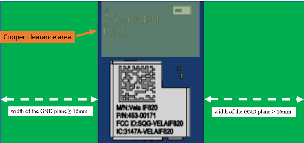
Antenna Keep-Out on Host PCB
For the integrated antenna variant, ensure the module is placed at the edge of the PCB and that there is adequate clearance around the antenna area. See layout diagrams (Figure 15) for reference.
External Antenna Integration
Refer to the regulatory sections for details on use of the Vela IF820 with external antennas in each regulatory region. See Certified Antennas for the list of certified external antennas.
Application Note for Surface Mount Modules
Introduction
Ezurio's surface mount modules are designed to conform to all major manufacturing guidelines. This application note is intended to provide additional guidance beyond the information that is presented in the user manual. This application note is considered a living document and will be updated as new information is presented.
The modules are designed to meet the needs of several commercial and industrial applications. They are easy to manufacture and conform to current automated manufacturing processes.
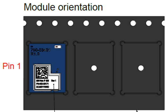
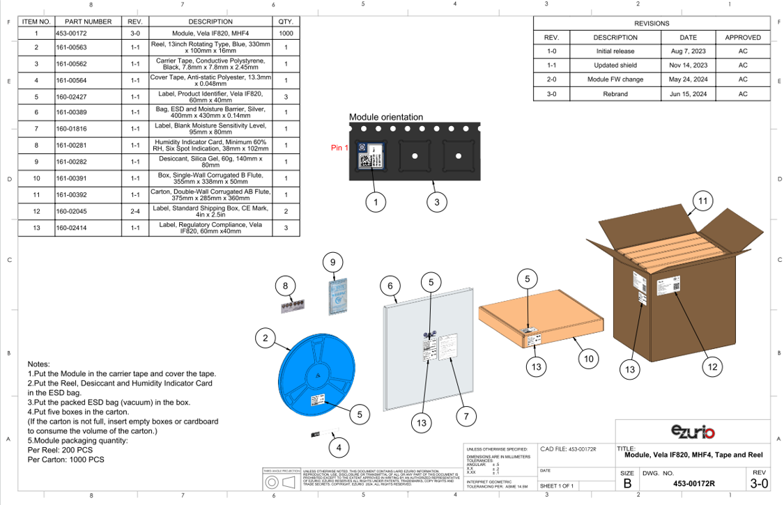
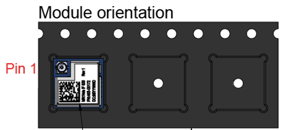
Vela IF820 part numbers 453-00171R and 453-00172R are shipped as Tape / Reel, with a reel containing 1,000 pcs.
Module Packaging Configuration
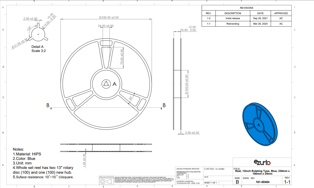
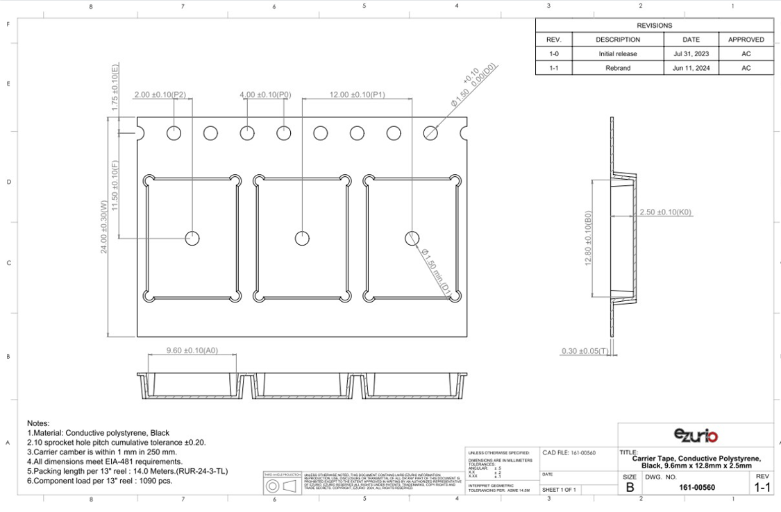
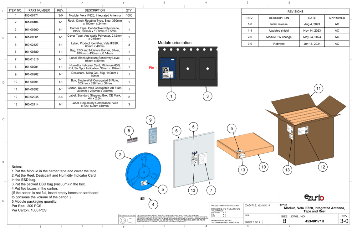
Reflow Parameters
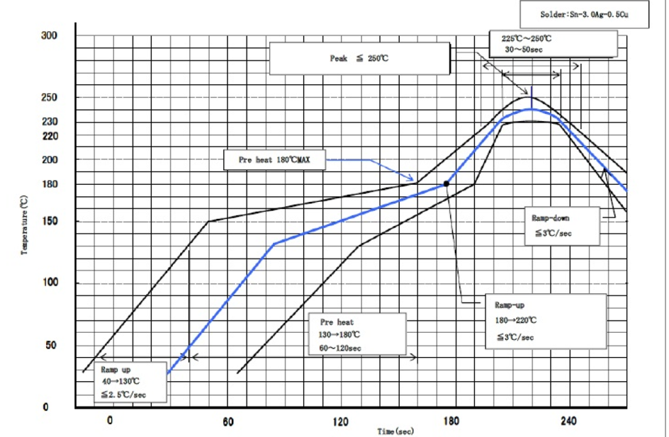
The following soldering conditions are recommended to ensure device quality.
Note: When soldering, the stencil thickness should be ≥ 0.1 mm.
Convection reflow or IR/Convection reflow (one-time soldering or two-time soldering in air or nitrogen environment):
- Measuring point — IC package surface
- Ramp-up: 40–130°C. Less than 2.5°C/sec
- Pre heat: 130–180°C 60–120 sec, 180°C MAX
- Ramp-up: 180–220°C. Less than 3°C/sec
- Peak Temperature: MAX 250°C — 225°C ~ 250°C, 30 ~ 50 sec
- Ramp-down: Less than 3°C/sec
Soldering Profile / Baking Conditions
Baking conditions and processes for the module follow the J-STD-033 standard which includes the following:
- The calculated shelf life in a sealed bag is 12 months at <40°C and <80% relative humidity.
- Once the packaging is opened, the SiP must be mounted (per MSL 4 / Moisture Sensitivity Level 4) within 72 hours at <30°C and <60% relative humidity.
- If the SiP is not mounted within 72 hours or if, when the dry pack is opened, the humidity indicator card displays >10% humidity, then the product must be baked for 48 hours at 125°C (±5°C).
Cautions when Removing the SIP from the Platform for RMA
- Bake the platform before removing the SIP from the platform. Reference baking conditions.
- Remove the SIP by using a hot air gun. This process should be carried out by a skilled technician.
Suggestion conditions:
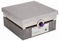
One-side component platform: Set the hot plate at 280°C. Put the platform on the hot plate for 8~10 seconds. Remove the SIP from platform.
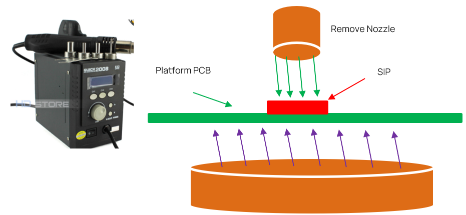
Two-side components platform: Use two hot air guns. On the bottom side, use a pre-heated nozzle (temperature setting of 200~250°C) at a suitable distance from the platform PCB. On the top side, apply a remove nozzle (temperature setting of 330°C). Heat the SIP until it can be removed from platform PCB.
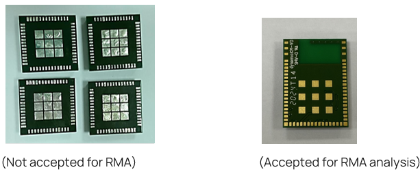
Remove the residue solder under the bottom side of SIP (alternate module pictured as an example).
- Remove and clean the residue flux as needed.
Precautions for Use
- Opening/handling/removing must be done on an anti-ESD treated workbench. All workers must also have undergone anti-ESD treatment.
- The devices should be mounted within one year of the date of delivery.
- The Vela IF820 modules are MSL 4 rated.
Shipping and Labeling
Packaging
All modules are shipped in tape and reel package and sealed in ESD Bags. Vela IF820 part numbers 453-00171R and 453-00172R are shipped as Tape / Reel, with a reel containing 1,000 pcs.
Labeling
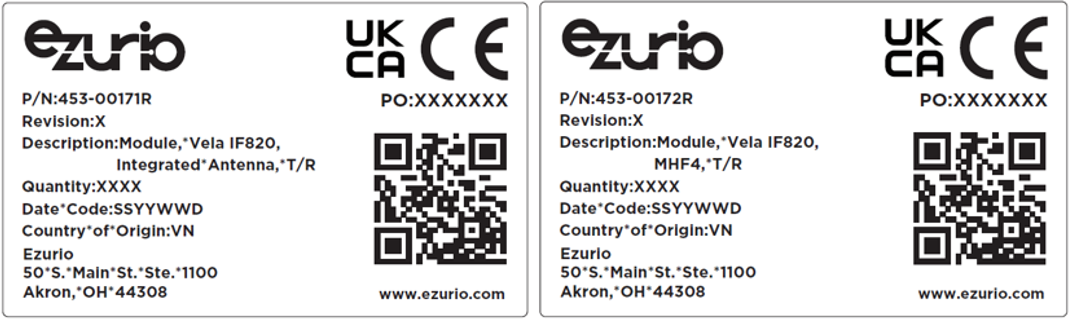
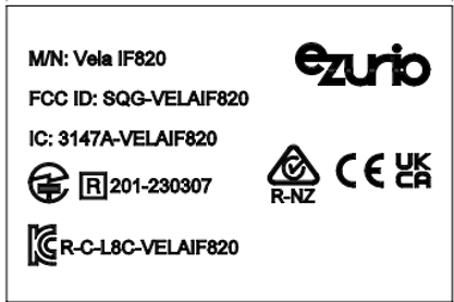
The following labels are placed on the anti-static bag. The Vela IF820 solder-down modules are classified as MSL4 devices.
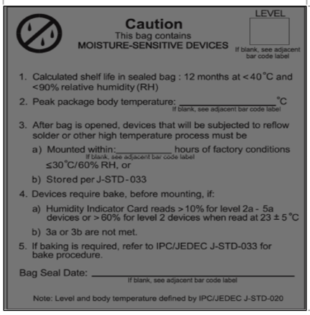
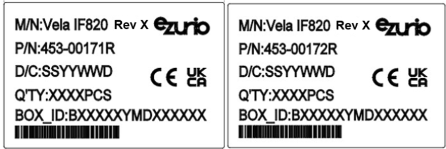
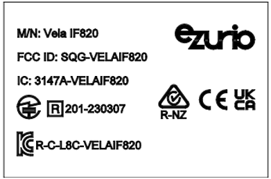
The following labels are placed on the pizza box.
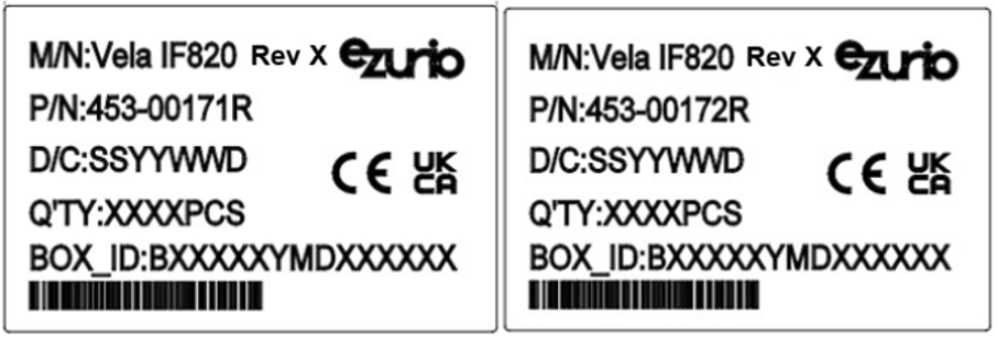
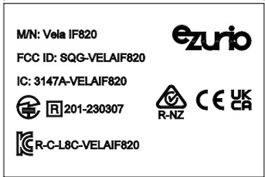
The following labels are placed on the master shipping carton.
Required Storage Conditions
Prior to Opening the Dry Packing
The following are required storage conditions prior to opening the dry packing:
- Normal temperature: 5~40°C
- Normal humidity: 80% (Relative humidity) or less
- Storage period: One year or less
Note: Humidity means relative humidity.
After Opening the Dry Packing
The following are required storage conditions after opening the dry packing (to prevent moisture absorption):
Storage conditions for one-time soldering:
- Temperature: 5–25°C
- Humidity: 60% or less
- Period: 72 hours or less after opening
Storage conditions for two-time soldering:
Storage conditions following opening and prior to performing the 1st reflow:
- Temperature: 5–25°C
- Humidity: 60% or less
- Period: A hours or less after opening
Storage conditions following completion of the 1st reflow and prior to performing the 2nd reflow:
- Temperature: 5–25°C
- Humidity: 60% or less
- Period: B hours or less after completion of the 1st reflow
Note: Should keep A+B within 72 hours.
Temporary Storage Requirements after Opening
- Only re-store the devices once prior to soldering.
- Use a dry box or place desiccant (with a blue humidity indicator) with the devices and perform dry packing again using vacuumed heat-sealing.
Storage period X1+X2 — refer to After Opening the Dry Packing storage requirements. Keep X1+X2 within 72 hours.

*** - External atmosphere temperature and humidity of the dry packing
- Storage period Y — keep within two weeks or less.
Environmental and Reliability
Reliability Tests
Environmental and Mechanical
Climatic and Dynamic
| Test Item | Specification | Standard | Test Result |
|---|---|---|---|
| Thermal Shock | Temperature: -40 ~ 85°C; Ramp time: Less than 10 seconds; Dwell Time: 10 minutes; Number of Cycles: 350 times | *JESD22-A106; *IEC 60068-2-14 for dwell time and number of cycles | Pass |
| Vibration | Non-Operating Unpackaged device; Vibration Wave Form: Sine Waveform; Vibration frequency / Displacement: 20–80 Hz/1.5mm; Vibration frequency / Acceleration: 80–2000 Hz/20g; Cycle Time: 4 min/cycle; Number of Cycles: 4 cycle/axis; Vibration Axes: X, Y and Z | JEDEC 22-B103B (2016) | Pass |
| Mechanical Shock | Non-Operating Unpackaged device; Pulse shape: Half-sine waveform; Impact acceleration: 1500 g; Pulse duration: 0.5 ms; Number of shocks: 30 shocks (5 shocks for each face); Orientation: Bottom, top, left, right, front, and rear faces | JEDEC 22-B110B.01 (2019) | Pass |
Reliability Prediction
| Ezurio Part Number | Environment | Standard | Test Result 45°C (Hours) |
|---|---|---|---|
| 453-00171R / 453-00171C | Ground, Fixed, Uncontrolled | Telcordia Issue 3 | 7,920,607 |
| 453-00172R / 453-00172C | Ground, Fixed, Uncontrolled | Telcordia Issue 3 | 8,084,775 |
| 450-00185 | Ground, Fixed, Uncontrolled | Telcordia Issue 3 | 1,114,640.34 |
| 453-00171R / 453-00171C | Mobile, Fixed, Uncontrolled | Telcordia Issue 3 | 2,970,228 |
| 453-00172R / 453-00172C | Mobile, Fixed, Uncontrolled | Telcordia Issue 3 | 3,031,791 |
| 450-00185 | Mobile, Fixed, Uncontrolled | Telcordia Issue 3 | 181,815.09 |
| Ezurio Part Number | Environment | Standard | Test Result 85°C (Hours) |
|---|---|---|---|
| 453-00171R / 453-00171C | Ground, Fixed, Uncontrolled | Telcordia Issue 3 | 1,839,958 |
| 453-00172R / 453-00172C | Ground, Fixed, Uncontrolled | Telcordia Issue 3 | 1,853,738 |
| 450-00185 | Ground, Fixed, Uncontrolled | Telcordia Issue 3 | 2,549,301.59 |
| 453-00171R / 453-00171C | Mobile, Fixed, Uncontrolled | Telcordia Issue 3 | 689,984 |
| 453-00172R / 453-00172C | Mobile, Fixed, Uncontrolled | Telcordia Issue 3 | 696,652 |
| 450-00185 | Mobile, Fixed, Uncontrolled | Telcordia Issue 3 | 440,892.82 |
Regulatory, Qualification & Certifications
Regulatory Approvals
Full regulatory information on the Vela IF820, including the Regulatory Information Guide, grants, and test reports are available on the Vela IF820 product page (coming soon).
The Vela IF820 holds current certifications in the following countries:
| Country/Region | Regulatory ID |
|---|---|
| USA (FCC) | SQG-VELAIF820 |
| EU (ETSI) | N/A (No ID Number Required) |
| UKCA | N/A (No ID Number Required) |
| Canada (ISED) | 3147A-VELAIF820 |
| Japan (MIC) | 201-230307 |
| Australia (RCM) | N/A |
| New Zealand (RCM) | N/A |
| Korea | R-C-L8C-VELAIF820 |
Certified Antennas
| Model | MPN | Manufacturer | Type | Connector | Peak Gain (2400–2500 MHz) |
|---|---|---|---|---|---|
| NanoBlue | EBL2400A1-10MH4L | Ezurio | PCB Antenna | IPEX MHF4 | 2 dBi |
| FlexPIFA | 001-0022 | Ezurio | Planar Inverted-F Type | IPEX MHF4 | 2 dBi |
| EDA-8709-2G4C1-B27-CY | EDA-8709-2G4C1-B27-CY (Ezurio Part# 0600-00057) | MAG.LAYERS | Dipole | IPEX MHF4 | 2.32 dBi |
| mFlexPIFA | EFA2400A3S-10MH4L | Ezurio | Planar Inverted-F Type | IPEX MHF4 | 2 dBi |
| AD1608 | AD1608-A2455AAT/LF | ACX | Chip Antenna | N/A | 1.0 dBi |
Bluetooth SIG Qualification
The Bluetooth Qualification Process promotes global product interoperability and reinforces the strength of the Bluetooth® brand and ecosystem to the benefit of all Bluetooth SIG members. The Bluetooth Qualification Process helps member companies ensure their products that incorporate Bluetooth technology comply with the Bluetooth Patent & Copyright License Agreement and the Bluetooth Trademark License Agreement (collectively, the Bluetooth License Agreement) and Bluetooth Specifications.
The Bluetooth Qualification Process is defined by the Qualification Program Reference Document (QPRD) v3.
To demonstrate that a product complies with the Bluetooth Specification(s), each member must for each of its products:
- Identify the product, the design included in the product, the Bluetooth Specifications that the design implements, and the features of each implemented specification
- Complete the Bluetooth Qualification Process by submitting the required documentation for the product under a user account belonging to your company
To complete the Qualification Process the company developing a Bluetooth End Product shall be a member of the Bluetooth SIG. To start the application please use the following link: Apply for Adopter Membership
Scope
This guide is intended to provide guidance on the Bluetooth Qualification Process for End Products that reference multiple existing designs, that have not been modified (refer to Section 3.2.2.1 of the Qualification Program Reference Document v3).
For a Product that includes a new Design created by combining two or more unmodified designs that have DNs or QDIDs into one of the permitted combinations in Table 3.1 of the QPRDv3, a Member must also provide the following information:
- DNs or QDIDs for Designs included in the new Design
- The desired Core Configuration of the new Design (if applicable, see Table 3.1 below)
- The active TCRL Package version used for checking the applicable Core Configuration (including transport compatibility) and evaluating test requirements
Any included Design must not implement any Layers using withdrawn specification(s). For the purposes of this document, it is assumed that the member is combining unmodified Core-Controller Configuration and Core-Host Configuration designs, to complete a Core-Complete Configuration.
Qualification Steps
For this qualification option, follow these steps:
- To start a listing, go to: https://qualification.bluetooth.com/
- Select Start the Bluetooth Qualification Process.
- Product Details to be entered: Project Name (this can be the product name or the Bluetooth Design name), Product Description, Model Number, Product Publication Date (the product publication date may not be later than 90 days after submission), Product Website (optional), Internal Visibility (this will define if the product will be visible to other users prior to publication). If you have multiple End Products to list then you can select 'Import Multiple Products', firstly downloading and completing the template, then by 'Upload Product List'. This will populate Qualification Workspace with all your products.
Specify the Design:
- Do you include any existing Design(s) in your Product? Answer Yes, I do.
- Enter the multiple DNs or QDIDs used in your design (for Option 2a two or more DNs or QDIDs must be referenced).
- Select 'I'm finished entering DNs'.
- Once the DNs or QDIDs are selected they will appear on the left-hand side, indicating the layers covered by the design (should show Core-Controller and Core Host Layers covered).
- What do you want to do next? Answer, 'Combine unmodified Designs'.
- The Qualification Workspace Tool will indicate that a new Design will be created and what type of Core-Complete configuration is selected.
- An active TCRL will be selected for the design.
- Perform the Consistency Check, which should result in no inconsistencies. If there are any inconsistencies these will need to be resolved before proceeding.
- Save and go to Test Plan and Documentation.
- Test Plan and Documentation: As no modifications have been made to the combined designs the tool should report the following message: 'No test plan has been generated for your new Design. Test declarations and test reports do not need to be submitted. You can continue to the next step.' Save and go to Product Qualification fee.
- Product Qualification Fee: Ensure a Prepaid Product Qualification fee is available as it is required at this stage to complete the Qualification Process. Prepaid Product Qualification Fees will appear in the available list so select one for the listing. If one is not available select 'Pay Product Qualification Fee'; payment can be done immediately via credit card, or you can pay via Invoice. Payment via credit card will release the number immediately; if paying via invoice the number will not be released until the invoice is paid. Once you have selected the Prepaid Qualification Fee, select 'Save and go to Submission'.
Submission:
- Some automatic checks occur to ensure all submission requirements are complete.
- To complete the listing any errors must be corrected.
- Once you have confirmed all design information is correct, tick all of the three check boxes and add your name to the signature page.
- Now select 'Complete the Submission'.
- You will be asked a final time to confirm you want to proceed with the submission, select 'Complete the Submission'.
- Qualification Workspace will confirm the submission has been submitted. The Bluetooth SIG will email confirmation once the submission has been accepted (normally this takes 1 working day).
- Download Product and Design Details (SDoC): You can now download a copy of the confirmed listing from the design listing page and save a copy in your Compliance Folder.
For further information, please refer to the following webpage: https://www.bluetooth.com/develop-with-bluetooth/qualification-listing/
Example Design Combinations
| Design Name | Owner | Declaration ID | QD ID | Link |
|---|---|---|---|---|
| Vela IF820 | Ezurio | D063148 | 217016 | https://qualification.bluetooth.com/ListingDetails/192311 |
| AIROC™ Bluetooth Host Software Stack | Infineon | D065385 | 223736 | https://qualification.bluetooth.com/ListingDetails/194929 |
Qualify More Products
If you develop further products based on the same design in the future, it is possible to add them free of charge. The new product must not modify the existing design (i.e. add ICS functionality), otherwise a new design listing will be required.
To add more products to your design, select 'Manage Submitted Products' in the Getting Started page, Actions, Qualify More Products. The tool will take you through the updating process.
Ordering Information
| Part | Description |
|---|---|
| 453-00171R | Vela IF820 - Dual Mode Bluetooth Module, Integrated Antenna (Infineon CYW20820) - Tape / Reel |
| 453-00171C | Vela IF820 - Dual Mode Bluetooth Module, Integrated Antenna (Infineon CYW20820) – Cut / Tape |
| 453-00172R | Vela IF820 - Dual Mode Bluetooth Module, MHF4 Connector (Infineon CYW20820) - Tape / Reel |
| 453-00172C | Vela IF820 - Dual Mode Bluetooth Module, MHF4 Connector (Infineon CYW20820) – Cut / Tape |
| 453-00171-K1 | Vela IF820 - Development Kit with integrated chip antenna |
| 453-00172-K1 | Vela IF820 - Development Kit with MHF4 Connector |
| 450-00185 | Vela IF820 - Dual Mode Bluetooth USB Adapter with integrated antenna variant (Infineon CYW20820) |
This is a preliminary datasheet. Please check with Ezurio for the latest information before commencing a design. If in doubt, ask. For additional information visit the Vela IF820 product page.
Additional Support & Appendices
Please contact your local sales representative or our support team for further assistance:
| Headquarters | Ezurio 50 S. Main St. Suite 1100 Akron, OH 44308 USA |
| Website | http://www.ezurio.com |
| Technical Support | http://www.ezurio.com/resources/support |
| Sales Contact | http://www.ezurio.com/contact |
Note: Information contained in this document is subject to change. Ezurio's products are subject to standard Terms & Conditions. © Copyright 2026 Ezurio All Rights Reserved. Any information furnished by Ezurio and its agents is believed to be accurate but cannot be guaranteed. All specifications are subject to change without notice. Responsibility for the use and application of Ezurio materials or products rests with the end user since Ezurio and its agents cannot be aware of all potential uses. Ezurio makes no warranties as to non-infringement nor as to the fitness, merchantability, or sustainability of any Ezurio materials or products for any specific or general uses. Ezurio or any of its affiliates or agents shall not be liable for incidental or consequential damages of any kind. All Ezurio products are sold pursuant to the Ezurio Terms and Conditions of Sale in effect from time to time, a copy of which will be furnished upon request. Nothing herein provides a license under any Ezurio or any third-party intellectual property right. Ezurio and its associated logos are trademarks owned by Ezurio and/or its affiliates.
Legacy - Revision History
| Version | Date | Notes | Contributors | Approver |
|---|---|---|---|---|
| 1.0 | 10 Oct 2023 | Initial release | Li Yuan Chang; Mark Duncombe; Rikki Horrigan; Ryan Erickson | Jonathan Kaye |
| 1.1 | 22 Jan 2024 | Updates to pin tables in MHF4 Connector Variant Module Pin Definition and Integrated Antenna Variant Module Pin Definition | Li Yuan Chang; Mark Duncombe; Rikki Horrigan; Ryan Erickson | Jonathan Kaye |
| 1.2 | 7 May 2024 | Add recommendation for 32.768KHz crystal. HCI UART IOs are required. | Li Yuan Chang; Ryan Erickson | Jonathan Kaye |
| 2.0 | 13 June 2024 | Ezurio rebranding. Added crystal connection diagram to Reference Schematic Design | Ryan Erickson; Sue White | Jonathan Kaye |
| 2.1 | 1 July 2024 | Fix the antenna gain in Certified Antennas | Li Yuan Chang | Jonathan Kaye |
| 2.2 | 15 Oct 2024 | Updates to Bluetooth Qualification | Dave Drogowski | Jonathan Kaye |