/filters:background_color(white)/2024-10/C625_4_OSMM_SOM_REV00-front.377.png)
/filters:background_color(white)/2026-02/Carbon-AM62L-TI351-front1.497.png)
/filters:background_color(white)/2024-12/CarbonAM67%20front.399.png)
/filters:background_color(white)/documentation/4063297636/15/Generic OSM Evaluation Kit.png)
Overview
The Ezurio OSM evaluation kit (EVK) is designed to prototype your integrated design using an Ezurio OSM module. The OSM module is soldered on the interposer board, which can connect to the OSM EVK by four 120 pin connectors. The Ezurio OSM EVK provides multiple display interfaces, camera, audio, CAN bus, M.2, Gigabit Ethernet and other hardware options for optimal flexibility and user experience.
This document describes key hardware aspects of the Ezurio OSM evaluation kit and is applicable to the EVK PCB with revision R5.0
Ezurio OSM Evaluation Kit Part Numbers
| Part Number | Product Description |
|---|---|
| EZCBC-000-0000-00000-2-K2 | OSM Evaluation Kit: Eval Board / HDMI Adapters / Eval Board / Antennas / Accessories / SOM sold separately |
Mechanical Specifications
| Specification | Description |
|---|---|
| Dimensions | 180 x 160 x 20.48 mm |
| Temperature Range | -40C to +85C |
Understanding the Evaluation Board
Block Diagram
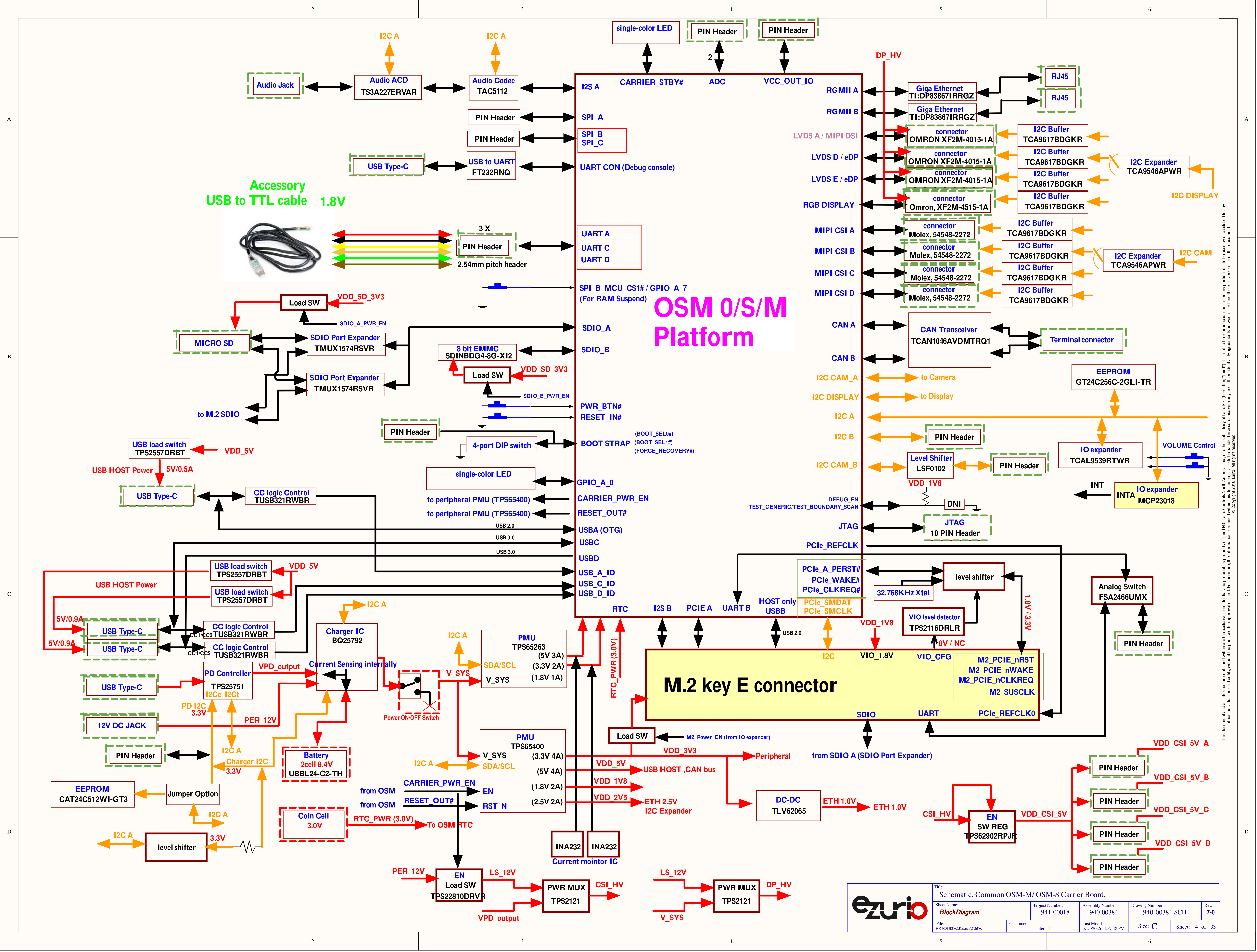
The figure below shows the block diagram of the Ezurio OSM evaluation board.
Understanding the Evaluation Board
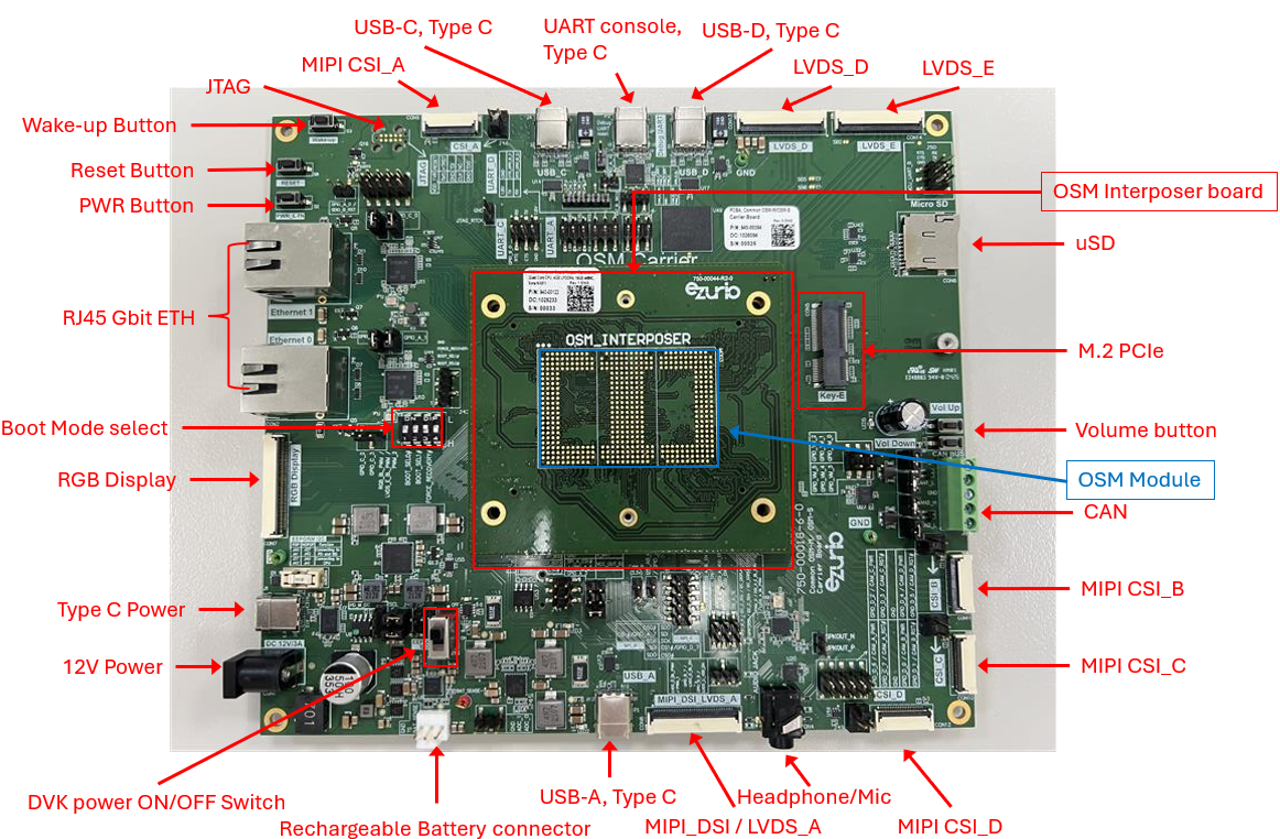
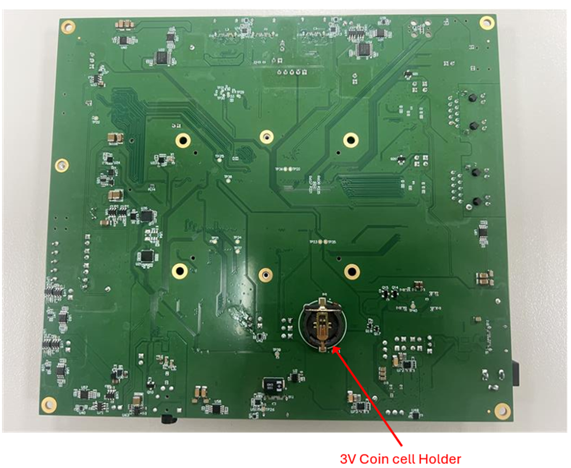
The OSM EVK images identify the locations of these key features and user interfaces (top and bottom view).
Interposer board
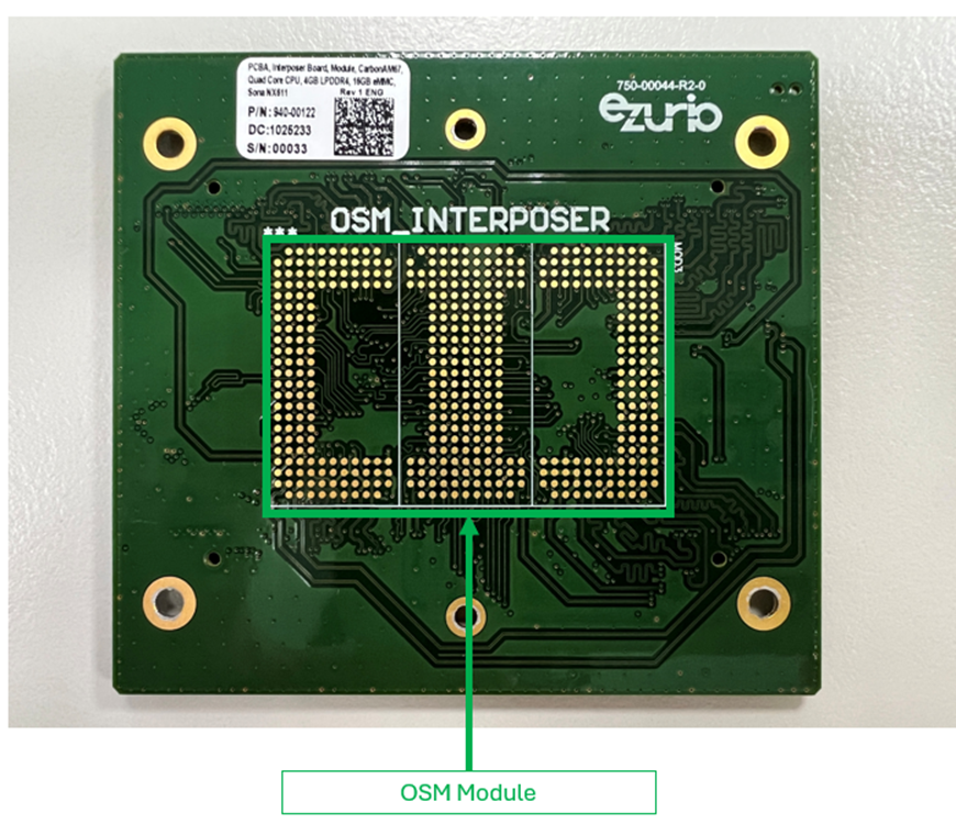
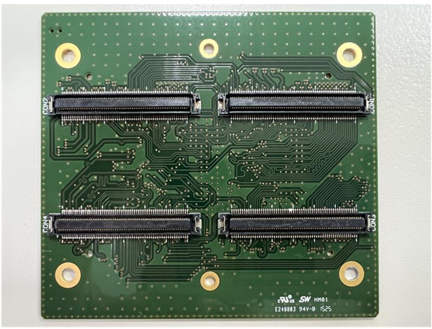
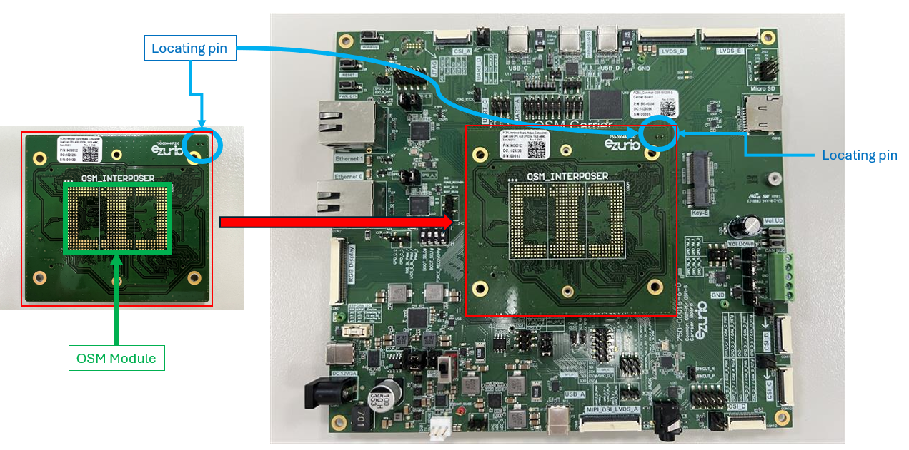
The interposer board is designed to replace various Ezurio OSM modules and connects to the OSM EVK via four 120-pin connectors. Please see the images below for the placement of the location pin on the interposer board for upright installation on the main board
Customers can adapt a single OSM EVK to different modules without purchasing a new EVK.
BOOT setting
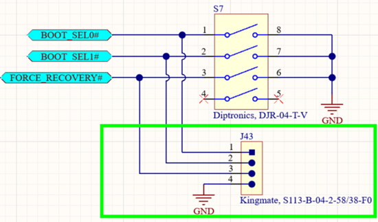
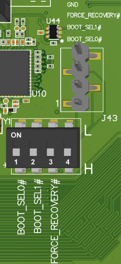
The OSM EVK provides three pins which can be set to different boot modes with switch S7. Slide switch S7 pin to “H” as open state, slide switch S7 pin to “L” as short to ground.
Please set the boot switches of the OSM EVK before powering OSM module.
J43 used to connected to external controller by fly bead if necessary.
| Connector pin | Boot pin name | OSM module pin |
|---|---|---|
| S7.1 (J43.1) | BOOT_SEL0# | U19 |
| S7.2 (J43.2) | BOOT_SEL1# | R18 |
| S7.3 (J43.3) | FORCE_RECOVERY# | T17 |
Key function Connectors
| Connector | Description | Vendor PN |
|---|---|---|
| CON15 CON16 CON17 CON18 | OSM Interposer Connector | Kyocera, 145046120640868+ |
| CON3 | Ethernet 1 | Kingconn, 7RJ45-F0-0332 |
| CON2 | Ethernet 0 | Kingconn, 7RJ45-F0-0332 |
| CON7 | RGB Display | Omron, XF2M-4515-1A |
| J1 | USB Type-C Power input | USB Type-C connector |
| CON1 | 12V DC input | DC Jack, SH, DC-005-2.0 |
| J3 | Rechargeable Battery connector | Molex, 22112032 |
| P1 | USB2.0 USB Type-C, OTG | USB Type-C connector |
| J4 J5 | USB3.0 USB Type-C, OTG | USB Type-C connector |
| CON6 | MIPI DSI / LVDS_A | Omron, XF2M-4015-1A |
| CON13 | LVDS_D | Omron, XF2M-4015-1A |
| CON14 | LVDS_E | Omron, XF2M-4015-1A |
| CON9 | MIPI_CSI_A | Omron, XF2M-2215-1A |
| CON11 | MIPI_CSI_B | Omron, XF2M-2215-1A |
| CON10 | MIPI_CSI_C | Omron, XF2M-2215-1A |
| CON12 | MIPI_CSI_D | Omron, XF2M-2215-1A |
| J46 | 5V power for CSI_A | Molex, 1718561002 |
| J48 | 5V power for CSI_B | Molex, 1718561002 |
| J45 | 5V power for CSI_C | Molex, 1718561002 |
| J49 | 5V power for CSI_D | Molex, 1718561002 |
| J9 | CAN BUS | Kingmate, ED350V-05P |
| CON5 | Key E M.2 | JAE, SM3ZS067U410AER1000 |
| CON8 | Micro SD Socket | Kingconn, 7MSDP-BA-1016 |
| P2 | UART debug console | USB Type-C connector |
| J24 | JTAG 10pin | Tag-Connect, TC2050-IDC-xx Default not fitted |
| CON4 | 3.5mm jack for Headphones | SJ-43515TS |
Functional Blocks
Power Supply
The following figure shows the OSM EVK Power Supply block.
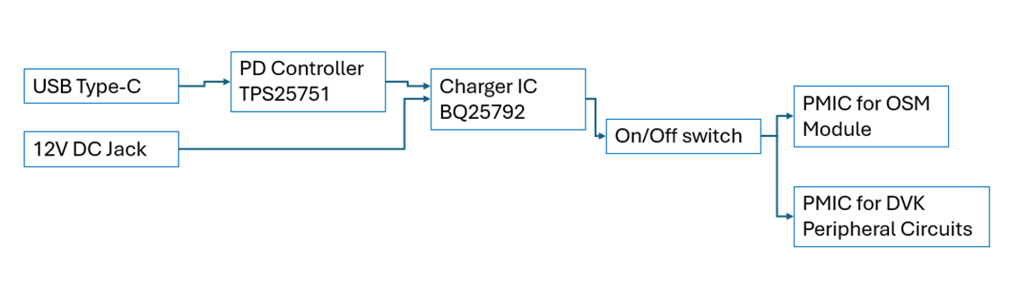
The OSM evaluation kit power-on procedure is as follows:
Select power source:E
- USB Type-C connector (J1) .Please use USB Type-C charger support up to 15V
- 12V DC Jack (CON1)
- Slide On/Off switch S1 to the on state.
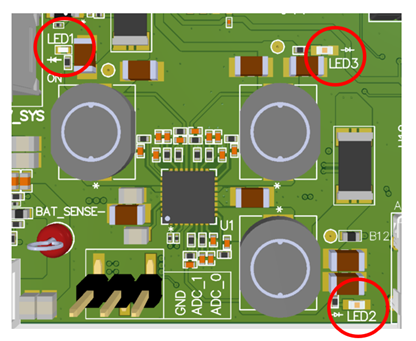
- Visually inspect the power LED1, LED2, LED3 is illuminated.
Warning: Switching between USB power and barrel jack power on the fly is not permitted.
Buttons
Wake-up Button
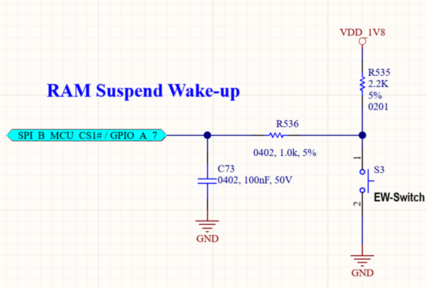
Button(S3) is designed to wake-up the OSM from RAM suspended mode. Please check the schematic below, which is shared with the OSM defined pin “SPI_B_MCU_CS1# / GPIO_A_7”.
RESET button
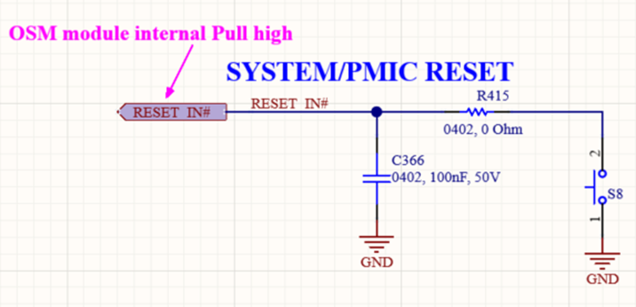
Button(S8) is designed to reset the module in OSM EVK. Please check the schematic below, which connects to OSM defined pin “RESET_IN#”.
PWR button
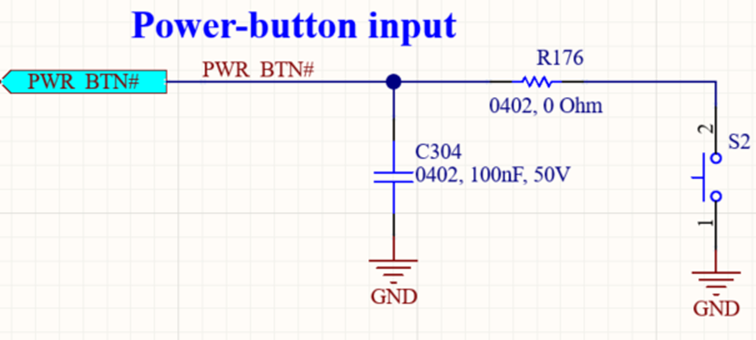
Button(S2) is designed to give power function to module in OSM EVK. Please check the schematic below, which connects to OSM defined pin “PWR_BTN#”.
Volume button
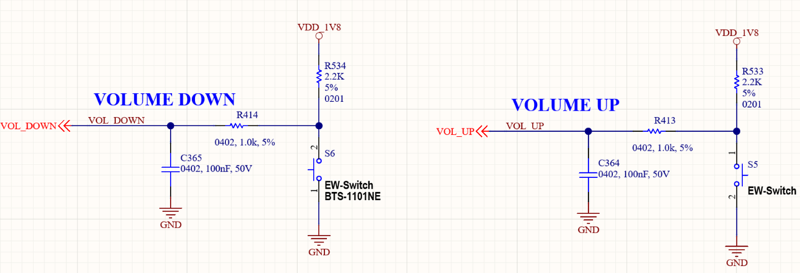
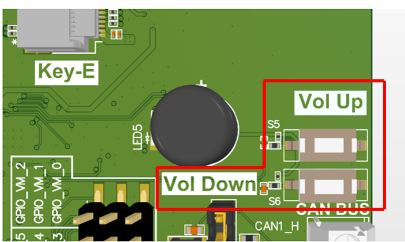
2 buttons (S5, S6) are designed for volume function in OSM EVK, 1 for volume up, 1 for volume down, both are connected to the IO expander (U21).
LED
| LED | Description |
|---|---|
| LED1 | OSM 5V power supply indication |
| LED2 | OSM 3.3V and SD card power supply indicator |
| LED3 | OSM 1.8V power supply indicator |
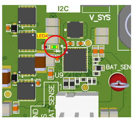
| LED4 | Indicates various BQ25792 (charger) operations. |
| LED5 | Indicates 3.3V for M.2 socket |
| LED8 | indicates CARRIER_STBY# status. |
| LED10 | Controlled by GPIO_A_0 |
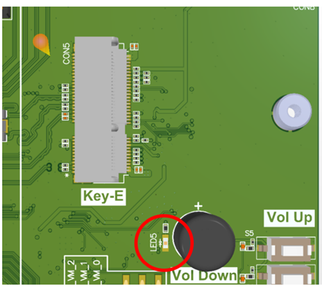
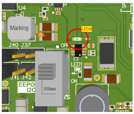
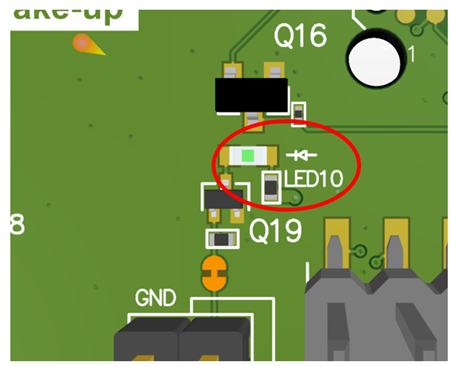
ETHERNET
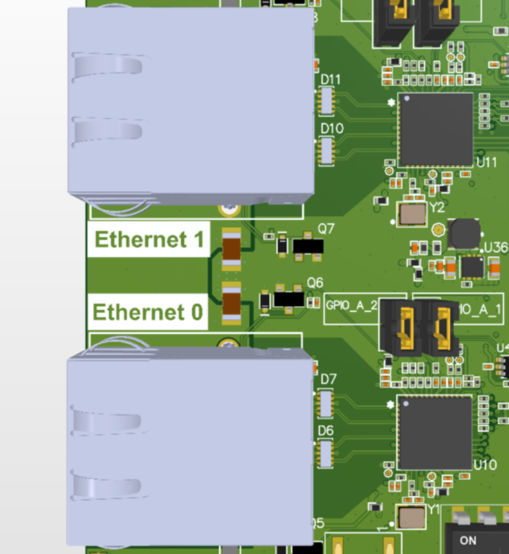
The OSM EVK is equipped with two 1 Gb (10/100/1000) DP83867 Ethernet PHY over RGMII1 and RGMII2, and each of them uses RJ45 ethernet connector (CON2 : Ethernet0, CON3 : Ethernet1) with integrated magnetics.
RGB Display
RGB signal
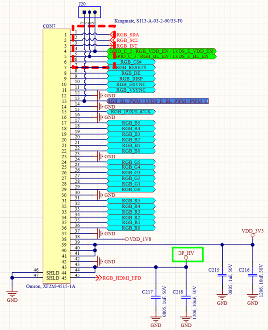
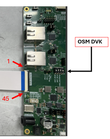
OSM EVK supports one 18bit RGB signal from OSM module to CON7. Please note CON7 is designed with 45 pins with a dual-side contact connector.
RGB to HDMI adapter board
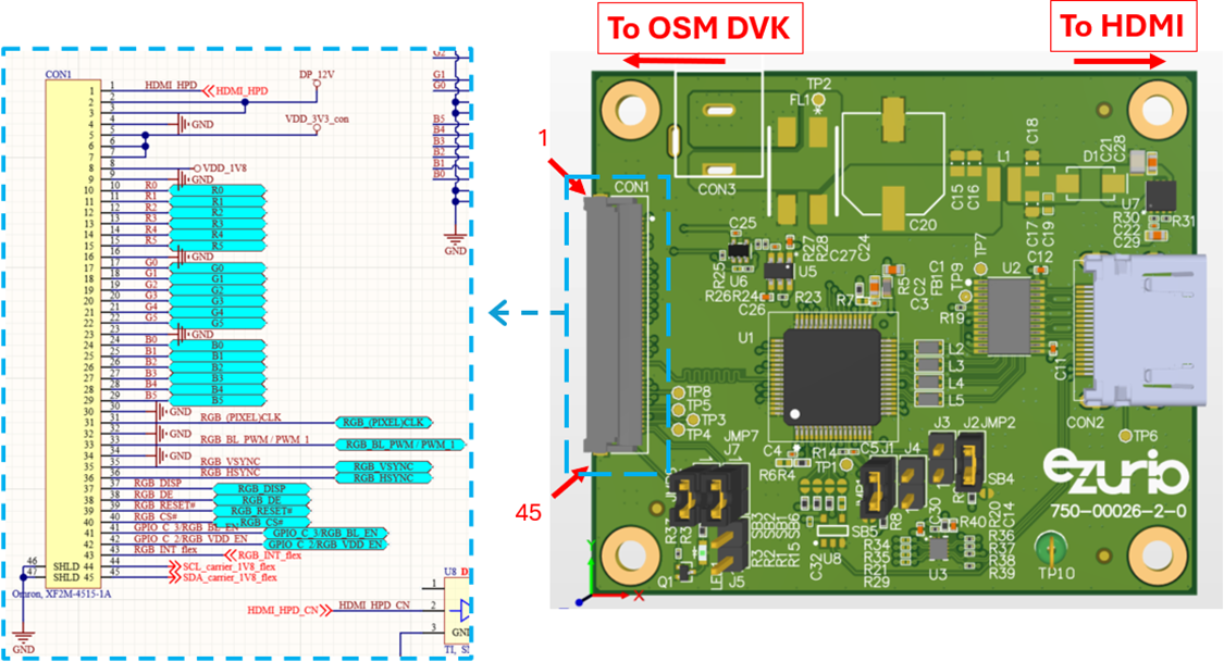
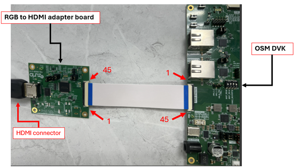
Ezurio offers an adapter board which can transfer 18-bit RGB signal to HDMI via 45 pin flex cable, please see the detail and the setup below.
Rechargeable Battery Support
OSM EVK provides a 3 pins connector for rechargeable lithium-polymer battery usage, please see schematic below.
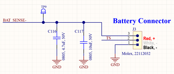
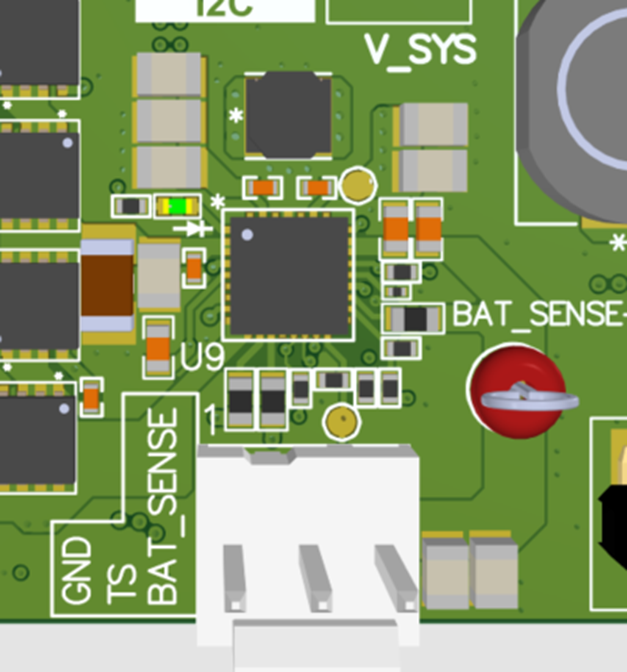
The following is the default support battery models and specification, please contact Ezurio whether another rechargeable battery can be used.
| Manufacture | MPN | brief description |
|---|---|---|
| ULTRALife | UBBL24-FL-TH | Battery Packs LI-ION 7.2V 4.8AH CONN W/THERMISTER |
USB Interface
USB_A
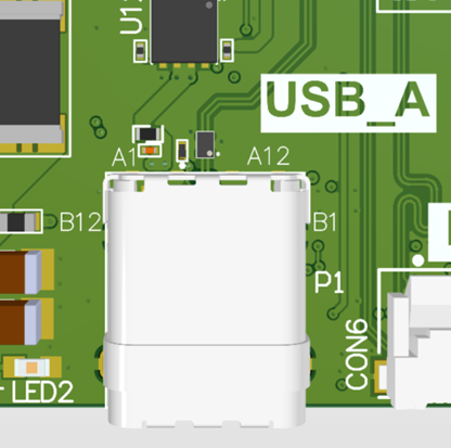
The OSM EVK provides a USB2.0 port on USB_A with a USB-C connector (P1). It’s designed for OTG function with maximum sourcing current 500mA.
USB_C & USB_D
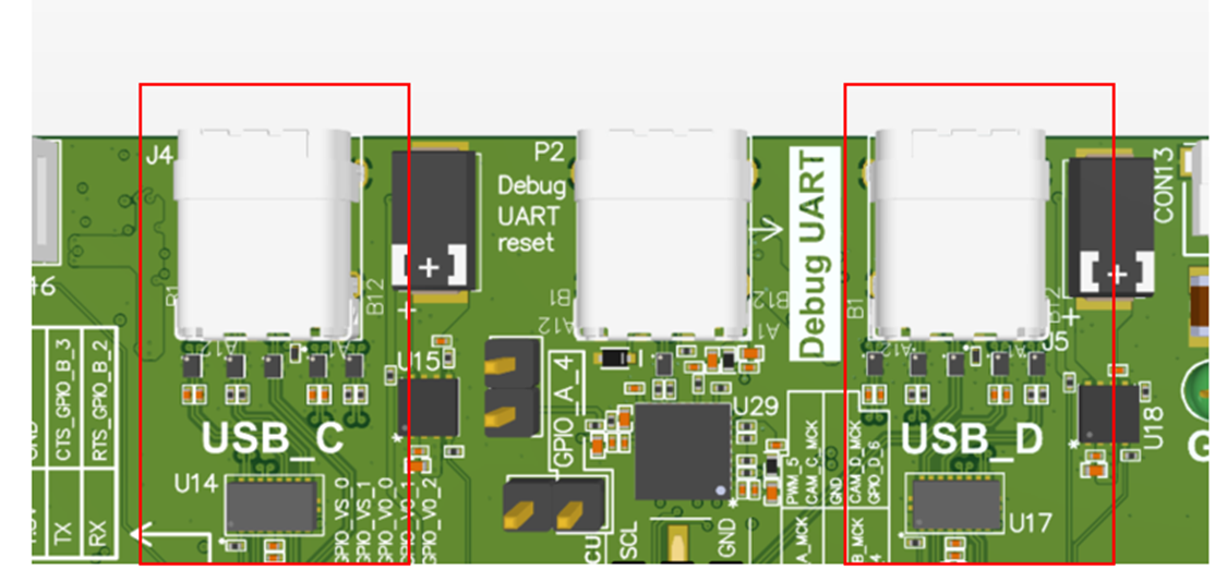
The OSM EVK provides two USB3.0 ports on USB_C and USB_D with USB Type-C connector (J4, J5). It’s designed for OTG function with maximum sourcing current 900mA.
MIPI DSI
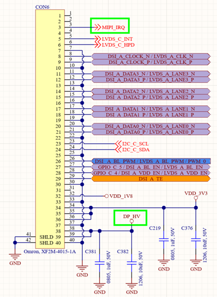
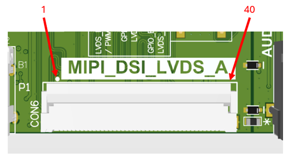
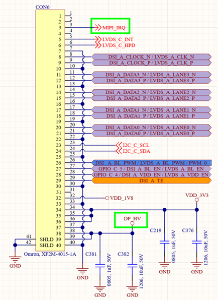
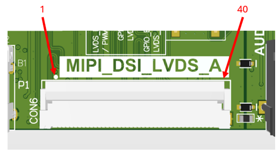
The OSM EVK provides a 4 lane MIPI-DSI connector (CON6) driven by the MIPI-DSI signals from the OSM module. Please note CON6 is designed with 40 pinouts with a double-sided contact connector.
MIPI DSI to HDMI adapter board
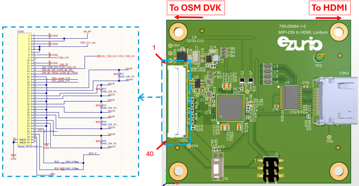
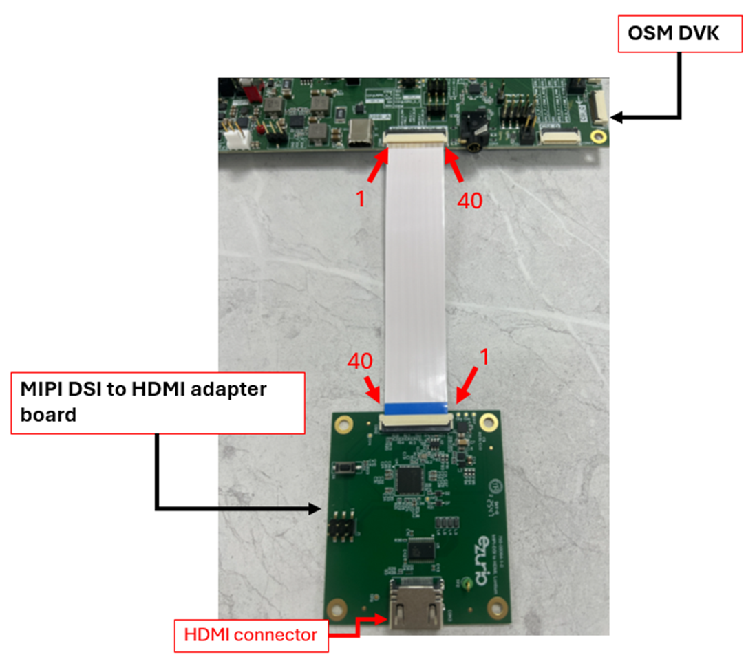
Ezurio offers an adapter board which can transfer MIPI DSI signal to HDMI signal, please see the setup below.
MIPI-DSI to Ezurio MIPI Display
Ezurio offers an adapter board which can transfer MIPI DSI signal to Ezurio MIPI interface display, please see the setup below.
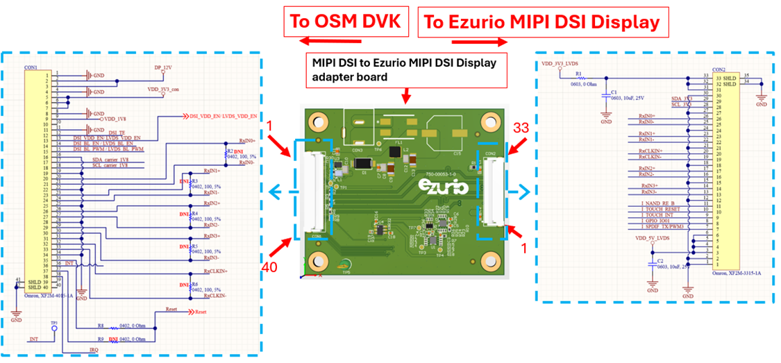
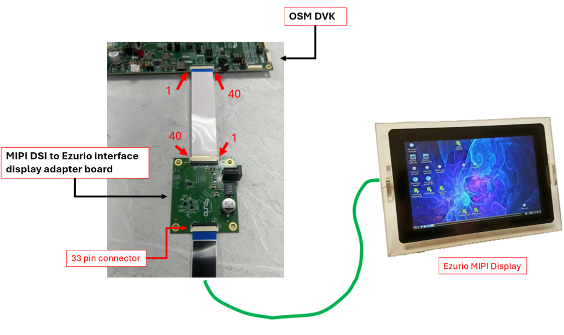
Please see the Ezurio MIPI interface display information below. More details on Ezurio displays can be found on our website: Displays | Ezurio
| Ezurio Display part number | Size |
|---|---|
| BD070LIC3_MIPI | 7 inch |
| BD101LCC3_MIPI | 10 inch |
LVDS
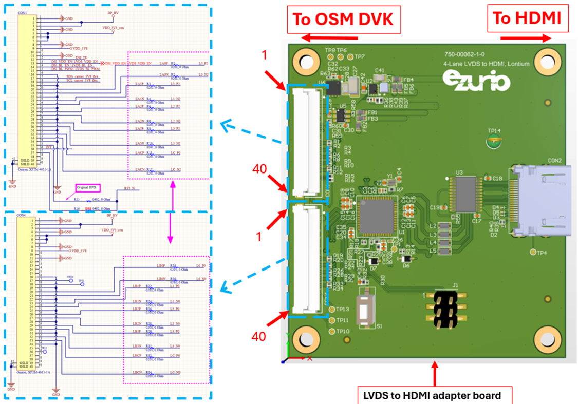
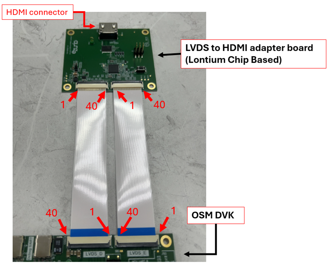
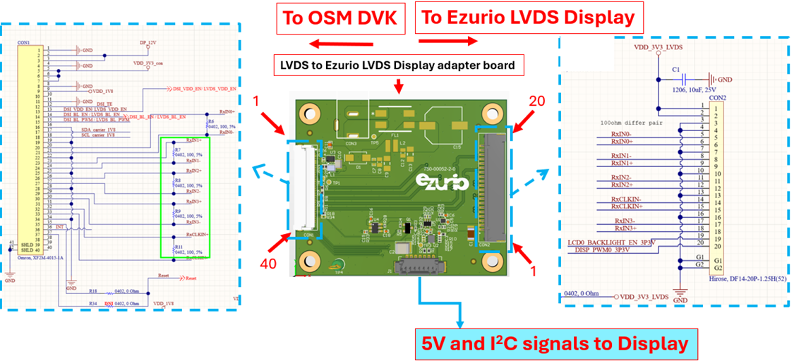
The OSM EVK provides three 4-lane LVDS connectors (CON6, CON13, CON14) driven by the LVDS signals from the OSM module. Please note CON6 is shared with MIPI DSI signals and all these connectors are designed with 40 pinouts with a double-sided contact connector.
LVDS_D & LVDS_E
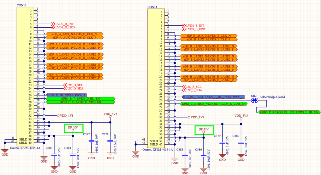
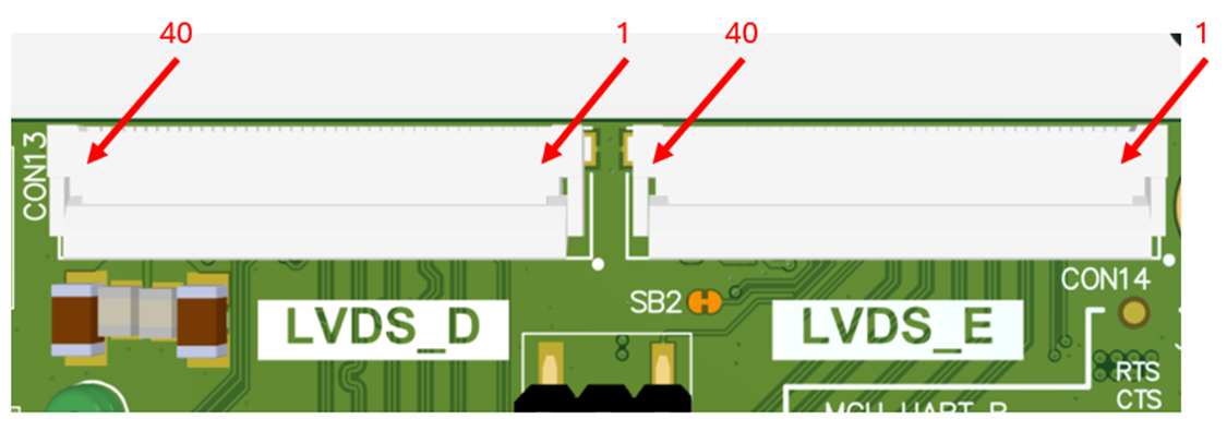
LVDS to HDMI adapter board
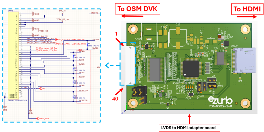
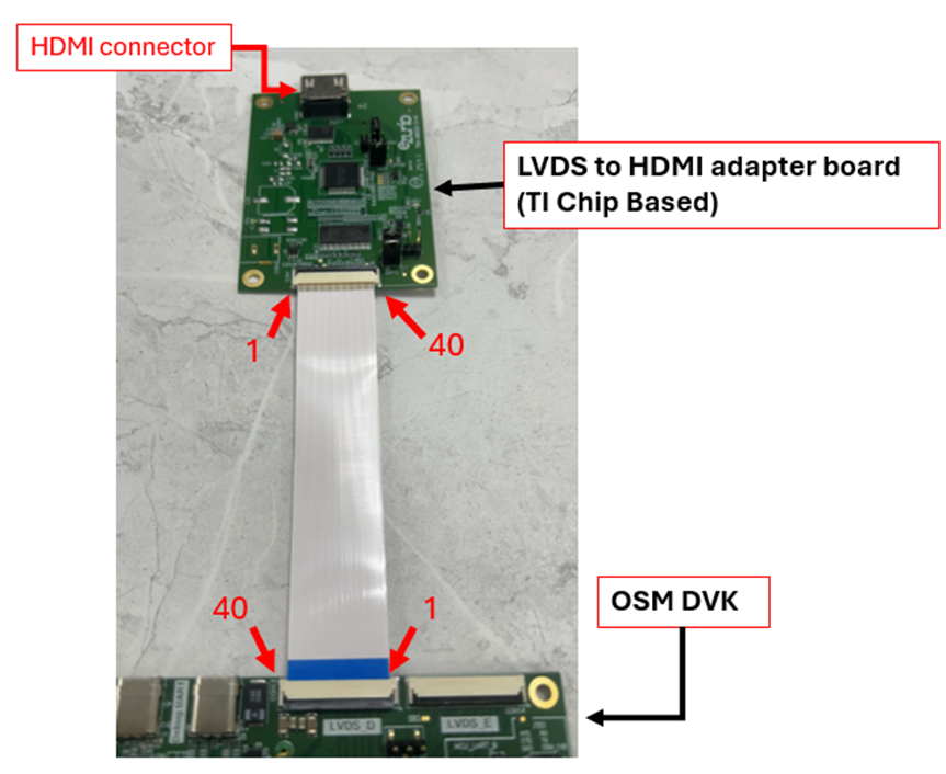
Ezurio offers two kinds of adapter boards which can transfer LVDS signal to HDMI, please see the setup below.
TI chip based - Support for up to 595Mbps per data lane
Lontium chip based - 1 or 2 ports configuration can be set, supporting up to 1.5Gbps per data lane.
LVDS to Ezurio LVDS Display adapter board
Ezurio offers an adapter board which can transfer LVDS signal to an Ezurio LVDS interface display, please see the setup below.
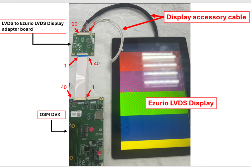
Please check the Ezurio LVDS interface display information below. More detail on our displays can be found on our website: Displays | Ezurio.
| Ezurio Display part number | size |
|---|---|
| BD070LIC3 | 7 inch |
| BD101LCC3 | 10 inch |
Audio
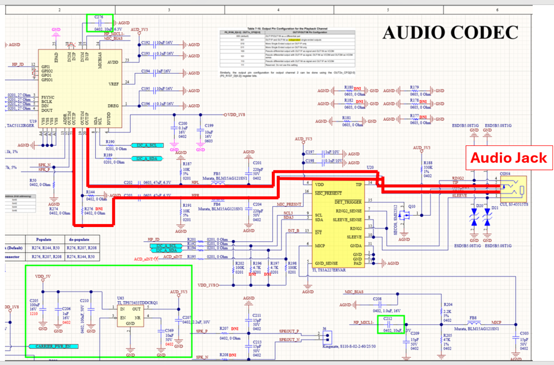
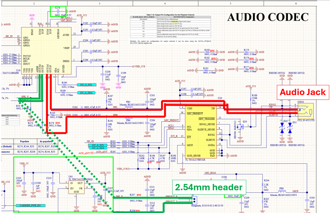
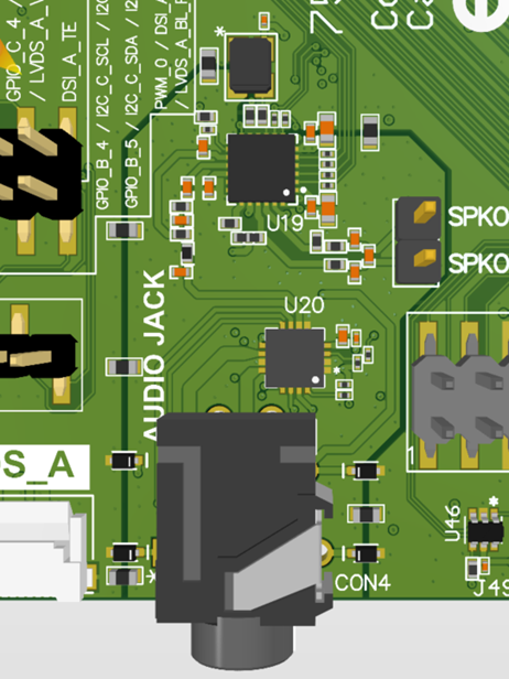
The OSM EVK supports audio with one input/two outputs via a 3.5mm audio jack and 2.54mm pin header. The circuit includes a codec (TAC5112) and audio accessory detection (TS3A227E).
For Output Channel Configurations, it can be configured as differential outputs or single-ended outputs for playback channels. The default setting is single-ended output to an audio jack. Resistor rework on the OSM EVK is needed if attempting to modify to differential outputs.
| Configuration | Populate | de-populate |
|---|---|---|
| Single-ended output (default) | R274, R144, R50 | R276, R207, R208 |
| Differential outputs | R276, R207, R208 | R274, R144, R50 |
Single-ended outputs : Codec Output1P and Output2P connect to Audio jack, Codec Output1M and Output2M connect to Ground
Differential-ended outputs : Codec Output1P and Output1M to Audio jack, Codec Output2P and Output2M to 2.54mm pin header
For recording function, 16 bit command is supported.
MIPI CSI
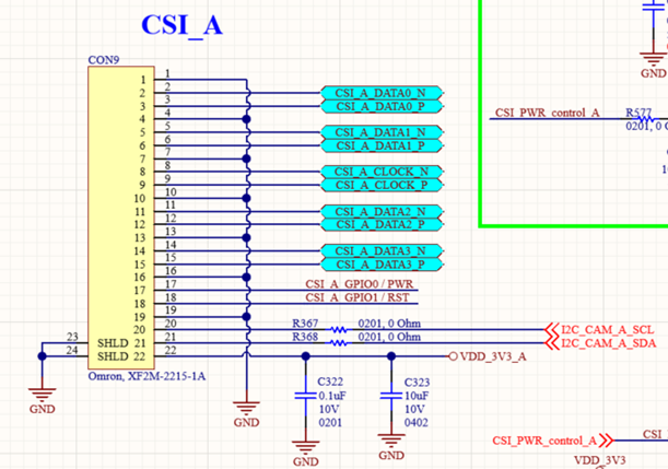
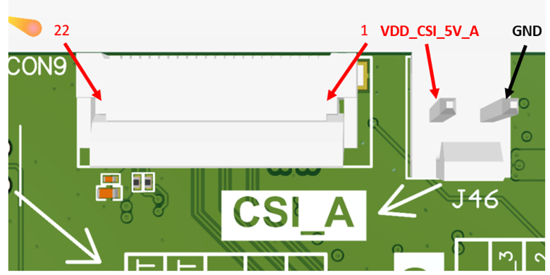
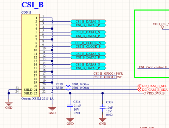
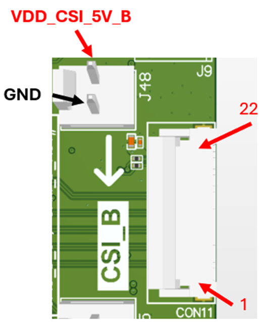
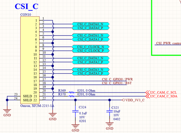
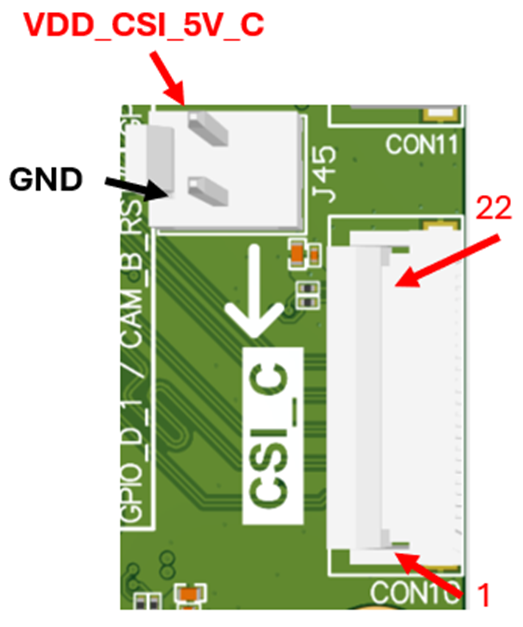
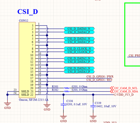
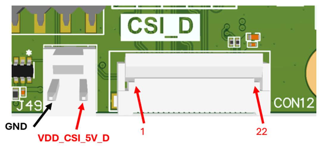
The OSM EVK provides four 22-pin connectors (CON9, CON10, CON11, CON12) which can support MIPI-CSI signal driven from OSM module. Additionally, each CSI signal has independent 5V support for advanced camera use if needed.
The OSM EVK by default supports two cameras as shown below.
| # of Cameras | Camera Supported |
|---|---|
| 1 | ArduCam B0582 (IMX678) |
| 2 | ArduCam B0562 (OV5645) |
CSI_A
CSI_B
CSI_C
CSI_D
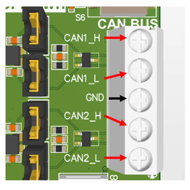
CAN BUS
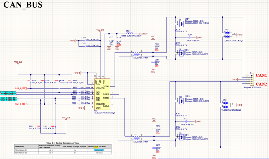
The OSM EVK supports two CAN BUS driven by CAN1 and CAN2 of the OSM modules. Both BUS on OSM EVK implement a 120ohm termination resistor. Default populated JMP7 and JMP8 support 120ohm termination on CAN1, default populated JMP10 and JMP11 support 120ohm termination on CAN2. You may populate or de-populate the jumpers based on your CAN application.
PCIE M.2
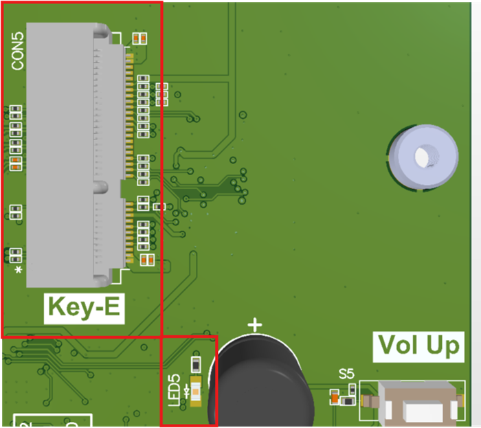
The OSM EVK implements Key-E M.2 PCIE connectors, which follow the PCI Express M.2 Specification.
LED5 is illuminated when VDD_3V3_M2 is enabled.
SDIO
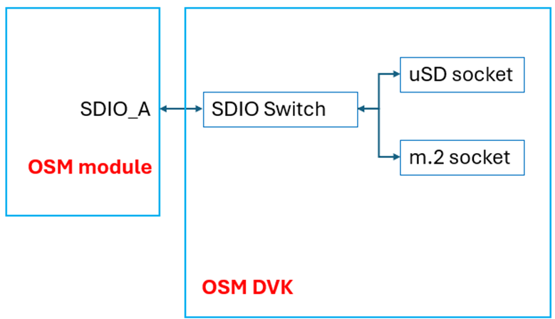
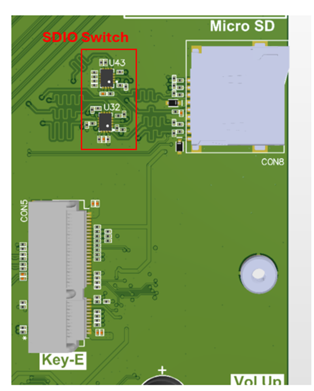
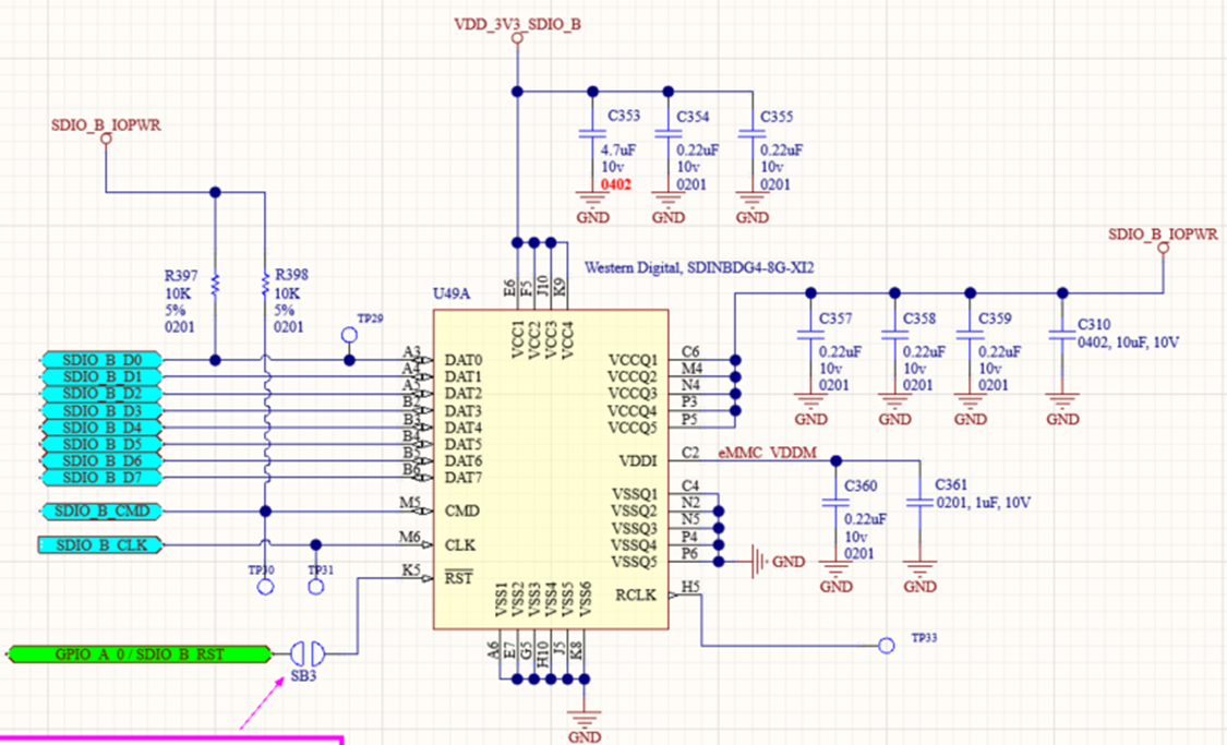
The OSM EVK supports two SDIO interfaces. One goes to microSD or M.2 connector by a SDIO switch, the other one goes to the on-board eMMC.
SDIO_A
Default path goes to microSD in order to support booting from an SD card. Customer can configure this to M.2 if needed in software.
SDIO_B
SDIO_B connects to the on-board eMMC.
SPI
The OSM EVK provides three exposed 2.54mm pin headers for SPI_A, SPI_B and SPI_C usage.
| SPI BUS | Connector | Schematic | Description |
|---|---|---|---|
| SPI_A | J44 and J27.1 | 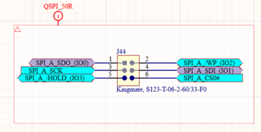 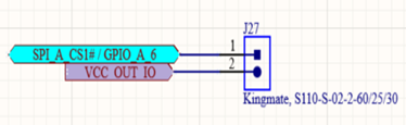 | SPI_A_CS1# shared with GPIO_A_6 |
| SPI_B | J19 pin 1,3,5,7,9 | 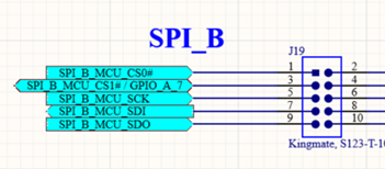 | SPI_B_MCU_CS1# shared with GPIO_A_7 |
| SPI_C | J19 pin 2,4,6,8,10 | 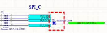 | SPI_C_CS1# shared with GPIO_D_7 |
RTC power
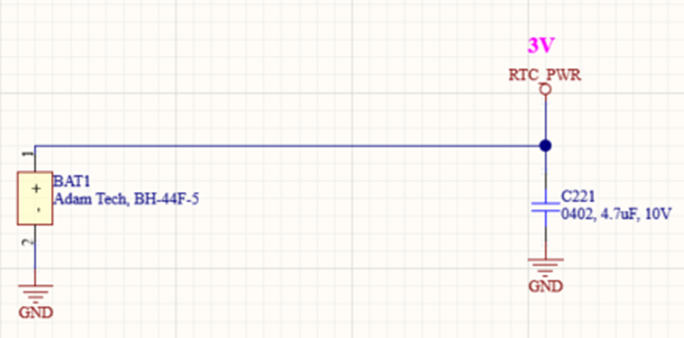
The OSM EVK provides a Coin Cell Battery Holders (BAT1) on the EVK backside, which connects to the OSM module pin RTC_PWR (W17). It is expected to have a 3V coin cell equipped.
JTAG
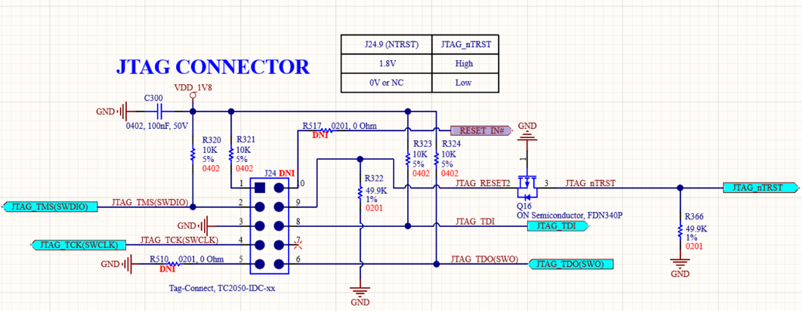
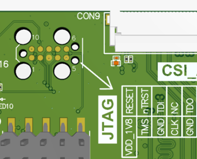
The OSM EVK provides a 10-pin TAG-Connect header on the EVK left-top side. Default is not populated.
DEBUG/TEST GENERIC/TEST BOUNDARY SCAN
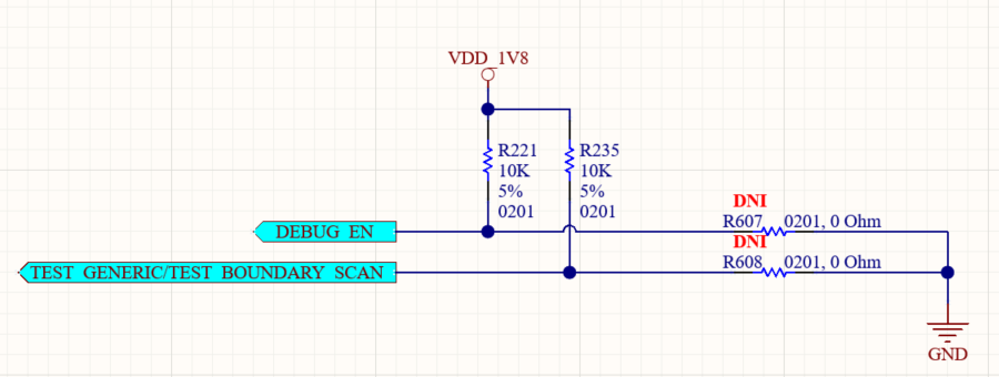
The OSM EVK provides default pull-ups for OSM defined pin “DEBUG_EN (module pin AC18)” and “TEST_GENERIC/TEST_BOUNDARY_SCAN (module pin C18)”. The user can also modify it to pull-down configuration using R607 and R608 by OSM test function requirement.
UART
The OSM EVK includes five UART ports (UART Debug Console, UART_A, UART_B_MCU, UART_C, UART_D) with different connectors, please see the detail below.
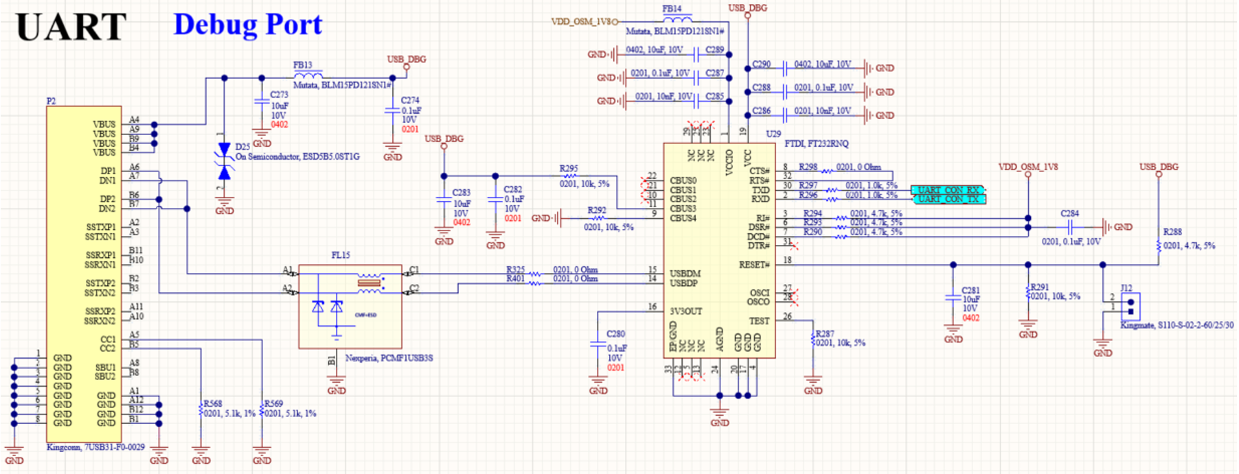
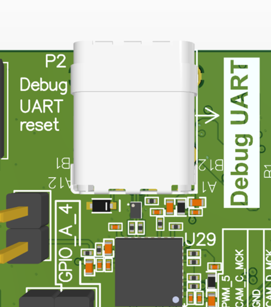
UART Debug Console
Transfer 2-wire debug UART signal from OSM module to USB Type-C connector(P2) by a FTDI bridge chip.
UART_A
Exposed 4-wire UART on the 2.54mm connector (J26).
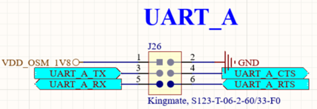
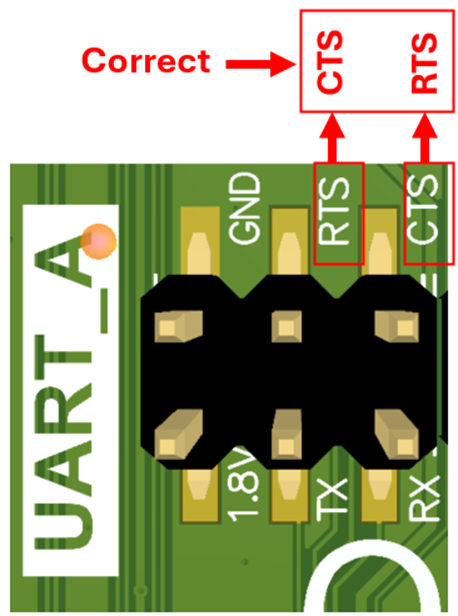
Note: Silkscreen on the RTS and CTS are opposite on PCB 5.0 and earlier versions. This will be fixed in future PCB versions.
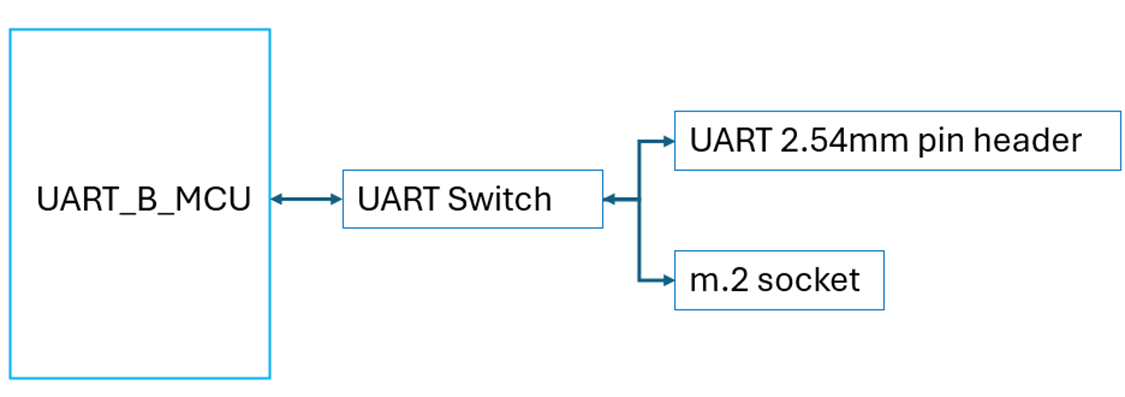
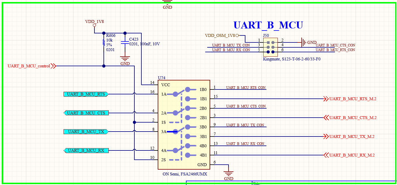
UART_B_MCU
The UART_B_MCU signals from the OSM module can be routed to either the 2.54 mm pin header or the M.2 connector via software configuration.
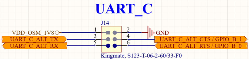
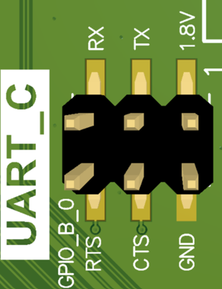
UART_C
Exposed 4-wire UART on the 2.54mm connector(J14).
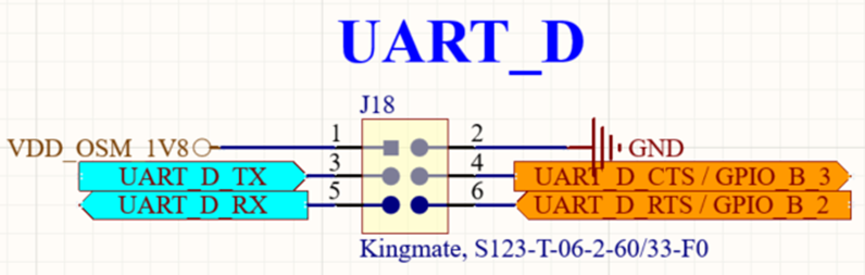
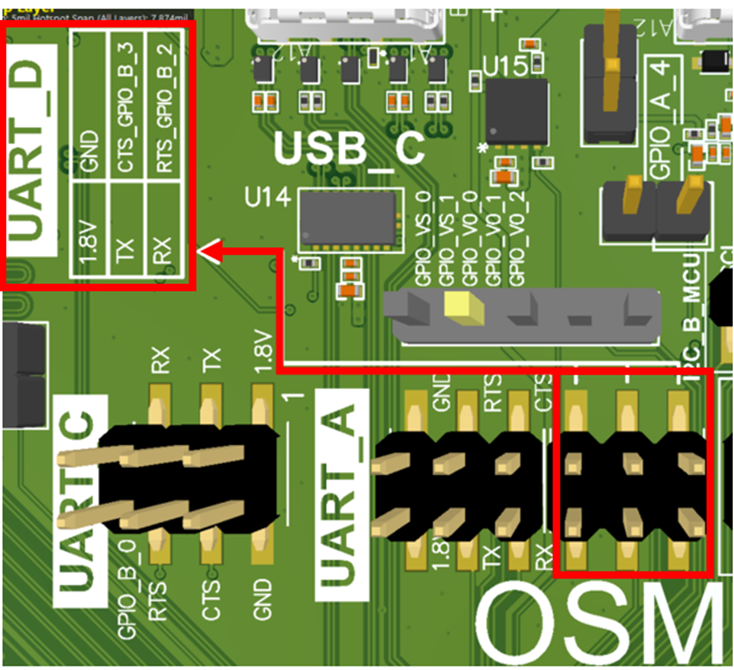
UART_D
Exposed 4-wire UART on the 2.54mm connector (J18).
I2C
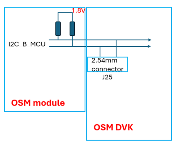
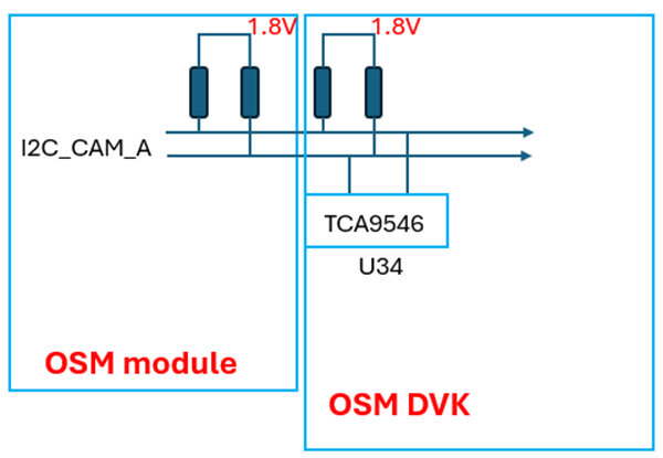
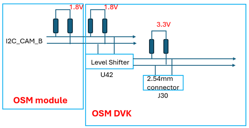
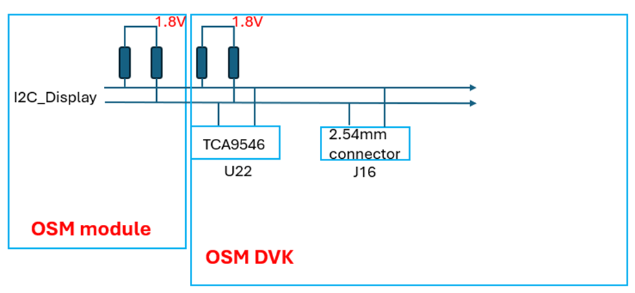
The OSM EVK includes five I2C interfaces (I2C_A, I2C_B_MCU, I2C_CAM_A, I2C_CAM_B, I2C Display), please see the details below.
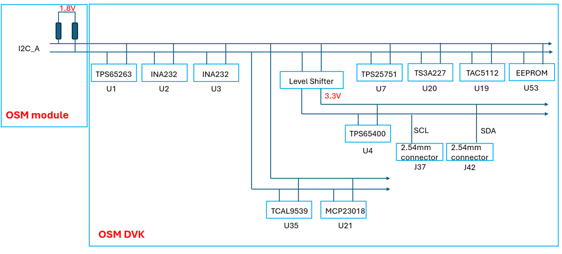
I2C_A
The OSM EVK uses I2C_A as primary I2C interface to access multiple devices on EVK, please see the I2C_A tree. Additionally, the exposed J37 pin2 (I2C_A_SCL_3V3) and J42 pin1 (I2C_A_SDA_3V3) for user connects to I2C device. Please note these two pins already transfer to 3.3V.
I2C_B_MCU
The OSM EVK provides 2.54mm pin header connects to I2C_B_MCU.
I2C_CAM_A
The OSM EVK uses I2C_CAM_A from OSM module to access four CSI camera interfaces by an I2C switch.
I2C_CAM_B
The OSM EVK provides 2.54mm pin header connects to I2C_CAM_B, please note that working voltage already changes to 3.3V on this pin header.
I2C Display
The OSM EVK uses I2C_Display from OSM module to access to RGB/MIPI-DSI/LVDS interface by a I2C switch.
PWM
The OSM EVK provides an exposed pin header connection to the OSM PWM pin. Please see the details below.
| PWM name | Connector pin | Schematic | Description | OSM module pin |
|---|---|---|---|---|
| PWM_0 | J16.5 | 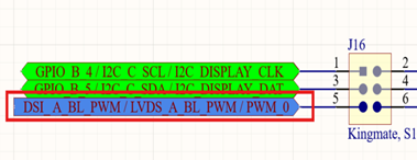 | PWM_0 shared with DSI_ A_BL_PWM / LVDS_A_BL_PWM | E18 |
| PWM_1 | J13.1 | 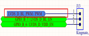 | PWM_1 shared with LVDS_D_BL_PWM | F18 |
| PWM_2 | J20.1 | 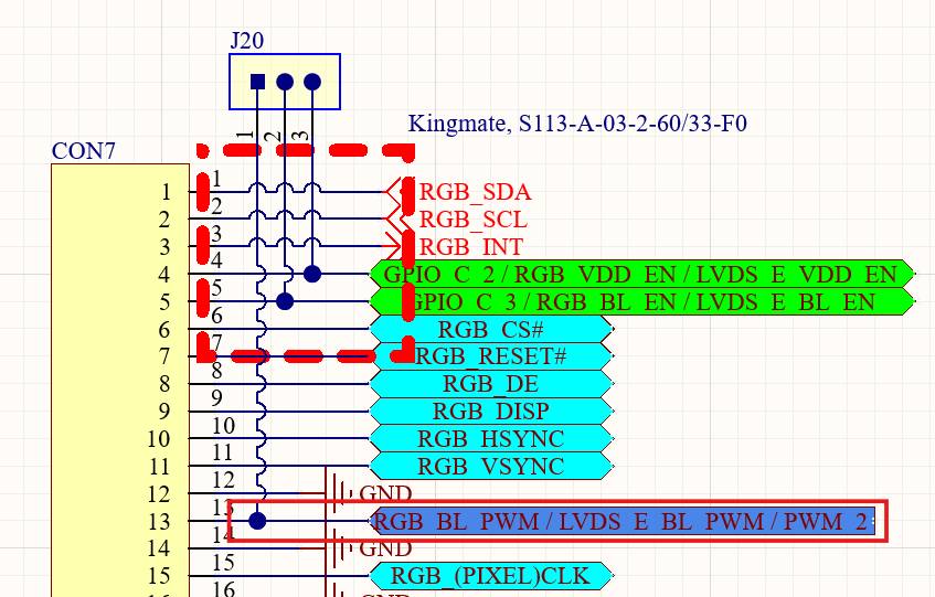 | PWM_2 shared with RGB_BL_PWM / LVDS_E_BL_PWM | G18 |
| PWM_3 | J28.5 | 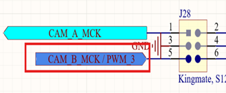 | PWM_3 shared with CAM_B_MCK | H18 |
| PWM_4 | J28.2 | 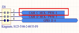 | PWM_4 shared with CAM_C_MCK | J18 |
| PWM_5 | J28.4 | 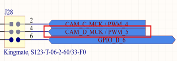 | PWM_5 shared with CAM_D_MCK | J18 |
MCK
The OSM EVK provides an exposed pin header connection to the OSM MCK pin. Please see the details below.
| MCK name | Connector Pin | Schematic | description | OSM module pin |
|---|---|---|---|---|
| CAM_A_MCK | J28.1 | 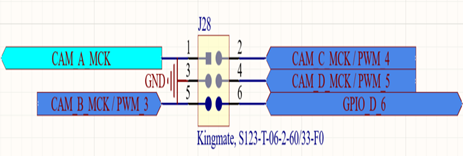 | CAM A Master Clock Output | C2 |
| CAM_B_MCK | J28.5 | CAM B Master Clock Output shared with PWM_3 | H18 | |
| CAM_C_MCK | J28.2 | CAM C Master Clock Output shared with PWM_4 | J18 | |
| CAM_D_MCK | J28.4 | CAM D Master Clock Output shared with PWM_5 | K18 |
GPIOs
The OSM EVK provides an exposed pin header connection to the OSM GPIO pin. Please see the details below.
| GPIO name | Connector Pin | Schematic | Description | OSM module pin |
|---|---|---|---|---|
| GPIO_A_0 | J51.1 | 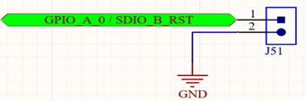 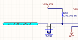 | GPIO_A_0 shared with LED control and SDIO_B_RST
| D17 |
| GPIO_A_1 | J31.2 | GPIO_A_1 shared with Ethernet_A_RST
| E17 | |
| GPIO_A_2 | J32.1 | 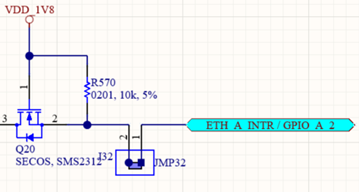 | GPIO_A_2 shared with Ethernet_A_INTR
| F17 |
| GPIO_A_3 | J36.1 | 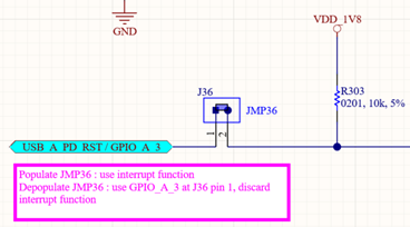 | GPIO_A_3 shared with IO expander interrupt
| G17 |
| GPIO_A_4 | J38.2 | 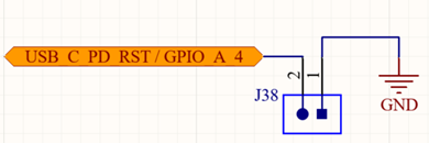 | JMP38.2 work as GPIO | H17 |
| GPIO_A_5 | J39.2 | 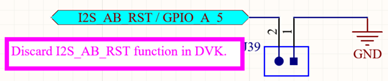 | JMP39.2 work as GPIO | J17 |
| GPIO_A_6 | J27.1 |  | JMP27.1 work as GPIO Shared with SPI_A_CS1# | K17 |
| GPIO_A_7 | J19.3 | 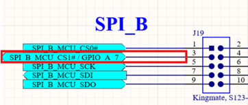 | GPIO_A_7 shared with RAM Suspend Wake-up button and SPI_B_MCU_CS1#
| L17 |
| GPIO_B_0 | J14.6 | 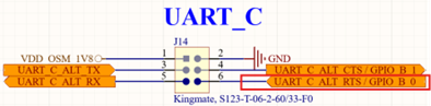 | GPIO_B_0 shared with UART_C_ALT_RTS
| D19 |
| GPIO_B_1 | J14.4 | 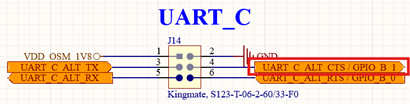 | GPIO_B_1 shared with UART_C_ALT_CTS
| E19 |
| GPIO_B_2 | J18.6 | 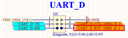 | GPIO_B_2 shared with UART_D_RTS
| F19 |
| GPIO_B_3 | J18.4 | 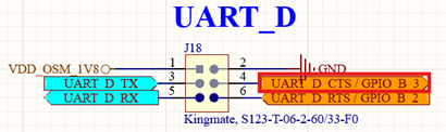 | GPIO_B_3 shared with UART_D_CTS
| G19 |
| GPIO_B_4 | J16.1 | 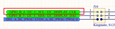 | GPIO_B_4 shared with I2C_C_CLK
| H19 |
| GPIO_B_5 | J16.3 | 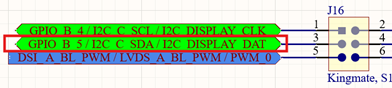 | GPIO_B_5 shared with I2C_C_CLK
| J19 |
| GPIO_B_6 | J13.3 | 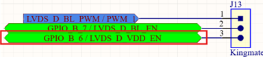 | GPIO_B_6 shared with LVDS_D_VDD_EN
| K19 |
| GPIO_B_7 | J13.2 | 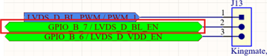 | GPIO_B_7 shared with LVDS_D_BL_EN
| L19 |
| GPIO_C_0 | J34.2 | 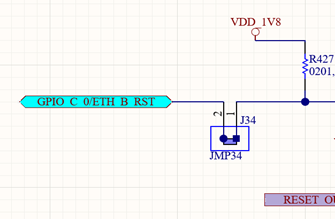 | GPIO_C_0 shared with Ethernet_B_RST
| D3 |
| GPIO_C_1 | J35.1 | 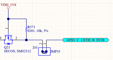 | GPIO_C_1 shared with Ethernet_B_INT
| D4 |
| GPIO_C_2 | J20.3 | 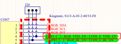 | GPIO_C_2 shared with RGB_VDD_EN / LVDS_E_VDD_EN
| E3 |
| GPIO_C_3 | J20.2 | 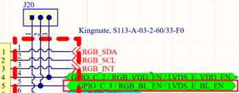 | GPIO_C_3 shared with RGB_BL_EN / LVDS_E_BL_EN
| E4 |
| GPIO_C_4 | J16.4 | 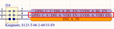 | GPIO_C_4 shared with DSI_A_VDD_EN / LVDS_A_VDD_EN
| F3 |
| GPIO_C_5 | J16.2 | 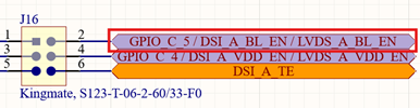 | GPIO_C_5 shared with DSI_A_BL_EN / LVDS_A_BL_EN
| F4 |
| GPIO_C_6 | J23.1 | 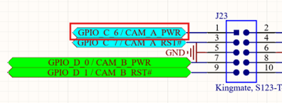 | GPIO_C_6 shared with CAM_A_PWR
| G3 |
| GPIO_C_7 | J23.3 | 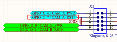 | GPIO_C_7 shared with CAM_A_RST#
| G4 |
| GPIO_D_0 | J23.7 | 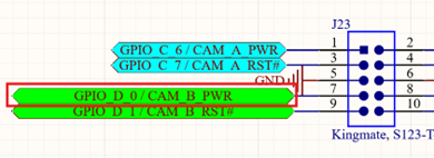 | GPIO_D_0 shared with CAM_B_PWR
| U32 |
| GPIO_D_1 | J23.9 | 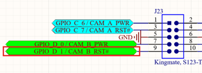 | GPIO_D_1 shared with CAM_B_RST#
| U33 |
| GPIO_D_2 | J23.2 | 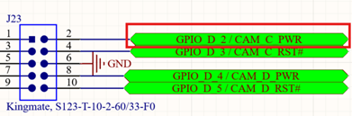 | GPIO_D_2 shared with CAM_C_PWR
| V32 |
| GPIO_D_3 | J23.4 | 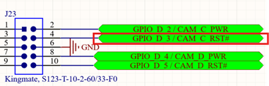 | GPIO_D_3 shared with CAM_C_RST#
| V33 |
| GPIO_D_4 | J23.8 | 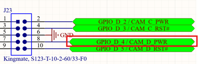 | GPIO_D_4 shared with CAM_D_PWR
| W32 |
| GPIO_D_5 | J23.10 | 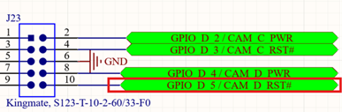 | GPIO_D_5 shared with CAM_D_RST#
| W33 |
| GPIO_D_6 | J28.6 | 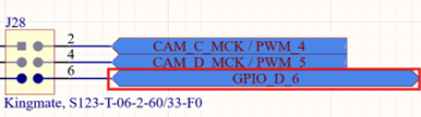 | JMP28.6 work as GPIO | Y32 |
| GPIO_D_7 | J28.6 | 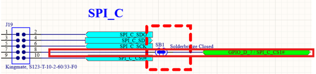 | GPIO_D_7 shared with SPI_C_CS1#
| Y33 |
Vendor Defined IO
The OSM EVK provides a pin header connecting to the OSM vendor defined pin. Please see the details below.
| Vendor Defined Pin Name | Connector Pin | Schematic | Description | OSM Module Pin |
|---|---|---|---|---|
| VENDOR DEFINED - SIZE-0 / GPIO_V0_0 | J17.3 | 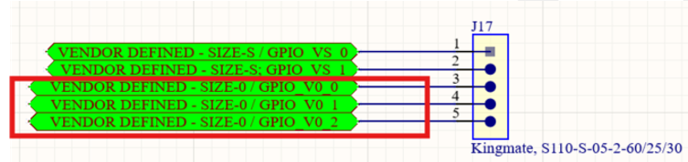 | Vendor Defined pin / GPIO_V0_0 | B22 |
| VENDOR DEFINED - SIZE-0 / GPIO_V0_1 | J17.4 | Vendor Defined pin / GPIO_V0_1 | C16 | |
| VENDOR DEFINED - SIZE-0 / GPIO_V0_2 | J17.5 | Vendor Defined pin / GPIO_V0_2 | P16 | |
| VENDOR DEFINED - SIZE-S / GPIO_VS_0 | J17.1 | 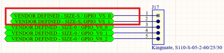 | Vendor Defined pin / GPIO_VS_0 | D6 |
| VENDOR DEFINED - SIZE-S / GPIO_VS_1 | J17.2 | Vendor Defined pin / GPIO_VS_1 | D7 | |
| VENDOR DEFINED - SIZE-M / GPIO_VM_0 | J21.1 |  | Vendor Defined pin / GPIO_VM_0 | Y29 |
| VENDOR DEFINED - SIZE-M / GPIO_VM_1 | J21.3 | Vendor Defined pin / GPIO_VM_1 | Y30 | |
| VENDOR DEFINED - SIZE-M / GPIO_VM_2 | J21.5 | Vendor Defined pin / GPIO_VM_2 | Y31 | |
| VENDOR DEFINED - SIZE-M / GPIO_VM_3 | J21.2 | Vendor Defined pin / GPIO_VM_3 | AA29 | |
| VENDOR DEFINED - SIZE-M / GPIO_VM_4 | J21.4 | Vendor Defined pin / GPIO_VM_4 | AA30 | |
| VENDOR DEFINED - SIZE-M / GPIO_VM_5 | J21.6 | Vendor Defined pin / GPIO_VM_5 | AA31 |