
Introduction
Overview
This document describes key hardware aspects of the BL5340. This document is intended to assist device manufacturers and related parties with the integration of this radio into their host devices. Data in this document is drawn from several sources. For full documentation on the BL5340, visit:
General Description
The BL5340 series of robust, tiny modules feature the Nordic nRF5340 SoC. It directly targets the highest performance with the lowest power budget, with additional variants featuring integrated Nordic nRF21540 PA/LNA for higher TX Power applications. Featuring Bluetooth 5.2 including Isochronous Channels and LE Audio, the BL5340 supports next generation Bluetooth audio for stereo streaming and broadcast audio.
The dual core Arm® Cortex M33 microcontrollers enable you to run a low power core focused purely on wireless connectivity, with a second higher performance core targeted for the end application itself. This further extends the multi-protocol capabilities of the product: Bluetooth LE, 802.15.4 (Thread / Zigbee) and NFC. It’s further enhanced with an ARM CryptoCell-312 including trusted execution, root-of-trust and secure key storage security features.
The BL5340 series brings out all nRF5340 hardware features and capabilities including USB access, up to +3 dBm transmit power, from 1.7V to 5.5V supply considerations, and a true industrial operating range of -40 to 105°C. Complete regulatory certifications enable faster time to market and reduced development risk completes Ezurio’s simplification of your next multi-protocol wireless design!
Note: BL5340 hardware provides all functionality of the nRF5340 chipset used in the module design. This is a hardware datasheet only – it does not cover the software aspects of the BL5340. This is to acknowledge that information in this datasheet is referenced from the nRF5340 datasheet – consult for details: https://infocenter.nordicsemi.com/topic/ps_nrf5340/keyfeatures_html5.html?cp=3_0_0
This datasheet is subject to change. Please contact Ezurio for further information.
Application Areas
- Medical devices
- IoT Sensors
- Access Control
- Health & Wellness devices
- Location awareness
- Factory automation
Features & Benefits
- Based on Nordic Semiconductor nRF5340 silicon
- Bluetooth v5.2 – Single mode
- NFC
- IEEE 802.15.4-2006 (Thread or Zigbee) radio support
- External or internal antennas
- Programmable Tx power +3 dBm to -20 dBm, -40 dBm
- Rx sensitivity -98 dBm (1 Mbps), - 104 dBm (125 kbps)
- Ultra-low power consumption
- Tx – 5.1 mA peak (at +3 dBm, DCDC on)
(See Note 1 in the Power Consumption section) - Rx: 2.7 mA peak (DCDC on)
(See Note 1 in the Power Consumption section) - System ON Idle – 1.3 uA typical
- System OFF – 0.9 uA – (See Note 4 in the Power Consumption section)
- UART, GPIO, ADC, PWM, timers, I2C, QSPI, SPI, I2S, PDM, and USB interfaces
- FCC, CE, ISED, RCM, MIC and UKCA certified
- Full Bluetooth Declaration ID
- Other regulatory certifications on request
- No external components required
- Industrial temperature range (-40° C to +105° C)
Specification Summary
Bluetooth
| Feature | Description |
|---|---|
| Frequency | 2.402 - 2.480 GHz for BLE (CH0 to CH39) 2.405 - 2.480 GHz for IEEE 802.15.4-2006 PHY (CH11 to CH26) |
| Maximum Transmit Power Setting (See Note 1 in the Module Specification Notes) | +3 dBm Conducted 453-00052 (Integrated antenna) +3 dBm Conducted 453-00053 (External antenna) |
| Minimum Transmit Power Setting | -40 dBm, -20 dBm (in 4 dB steps) -16 dBm, -12 dBm, - 8 dBm, - 7 dBm, -6 dBm, -5 dBm, -4 dBm, -3 dBm, -2 dBm, -1 dBm, 0dBm, +1dBm, +2dBm |
| Receive Sensitivity (≤37byte packet for BLE) | BLE 1 Mbps (BER=1E-3) -98 dBm typical BLE 2 Mbps -92 dBm typical BLE 125 kbps -104 dBm typical BLE 500 kbps -99 dBm typical IEEE 802.15.4-2006 250kbps -101 dBm typical |
| Raw Data Rates | 1 Mbps BLE (over-the-air) 2 Mbps BLE (over-the-air) 125 kbps BLE (over-the-air) 500 kbps BLE (over-the-air) 250 kbps IEEE 802.15.4 802.15.4-2006 (over-the-air) Nordic proprietary 1Mbps and 2Mbps modes (over-the-air) |
| Link Budget (conducted) | 101 dB @ BLE 1 Mbps 107 dB @ BLE 125 kbps |
| Bluetooth® | Bluetooth 5.2 – Single mode
|
Radio Performance
| Feature | Description |
| Antenna Options | |
| Internal | Printed PCB monopole antenna – on-board (453-00052 variant) |
| External |
See the Regulatory section and Regulatory Information Guide for FCC, ISED, MIC, RCM, UKCA and CE. The certified list of external antennas is listed in External Antenna Integration with the 453-00052 section. |
| IEEE 802.15.4-2006 PHY | 2405–2480 MHz IEEE 802.15.5-2006 radio transceiver, implementing IEEE 802.15.5-2006 compliant
|
| Nordic proprietary 1Mbps and 2Mbps modes radio (not currently certified by Ezurio) | 2402–2480 MHz Nordic proprietary 1Mbps and 2Mbps modes radio transceiver
|
| NFC | |
| NFC-A Listen mode compliant | Based on NFC forum specification
Modes of Operation:
Use Cases:
|
| System Wake-On-Field function | Proximity Detection |
Interfaces
| Feature | Description |
|---|---|
| Optional (External to the BL5340 module) |
| Host Interfaces and Peripherals | Applications Core (High Performance) | Network Core (ultra-low power) |
|---|---|---|
| Total | 48 x multifunction I/O lines | |
| Two co-processors | Arm Cortex-M33 with DSP, FPU, TrustZone support. 1024kB Flash 512kB RAM 8kB 2-way associative cache 128 and 64MHz clock Uses voltage and clock frequency scaling | Arm Cortex-M33 256kB Flash 64kB RAM 2kB instruction cache 64MHz clock |
| UART | 4 x UART (with CTS, RTS) | 1 x UART (with CTS, RTS) |
| USB | 1 x USB 2.0 FS (Full Speed, 12Mbps) | - |
| GPIO | Up to 48 32 x GPIOs on P0.00 to P0.31 15 x GPIOs on P1.00 to P1.15 With configurable I/O direction, O/P drive strength (standard 0.5 mA or high 3mA/5 mA), Pull-up /pull-down Input buffer disconnect | |
| ADC (200kbps) | Eight 8/10/12-bit channels on AIN0-AIN7 or VDD or VDDH/5 14-bit resolution with oversampling AIN0-AIN7 Configurable reference internal reference 0.6V or external reference VDD/4 Configurable pre-scaling of 4, 2, 1, 1/2, 1/3, 1/4, 1/5 1/6 Configurable acquisition time 3uS, 5uS, 10uS (default), 15uS, 20uS, 40uS. One-shot mode or Burst mode Scan mode for multiple channels Single ended or Differential or not connected | - |
| COMP | 1 x COMP (comparator) | - |
| LPCOMP | 1 x LPCOMP (low power comparator) | - |
| High-Speed SPI | 1 x High-speed SPI (32Mbps, SPIM4) master or slave with Easy DMA on dedicated pins | - |
| SPI | 4 x SPI (upto 16Mbps) master or slave with Easy DMA Slave is upto 8Mbps | 1 x SPI master or slave with Easy DMA Slave is upto 8Mbps |
| High-Speed TWI (I2C) | 1 x High-speed TWI (1Mbps) master or slave with Easy DMA on dedicated pins | 1 x High-speed TWI (1Mbps) master or slave with Easy DMA on dedicated pins |
| TWI (I2C) | 3 x TWI (upto 400kps, 200kbps, 100kbps) master or slave with Easy DMA | 1 x TWI (upto 400kps, 200kbps, 100kbps)) master or slave with Easy DMA |
| QSPI | 1 x QSPI interface (6 to 96MHz configurable clock frequency) for communicating with external flash memory. XIP (Execution in Place) capability. | - |
| PWM | 4 x PWM (pulse width modulation) units with Easy DMA | - |
| QDEC | 2 x QDEC (Quadrature decoder) | - |
| I2S | 1 x I2S (Inter-IC sound interface) | - |
| PDM | 1 x PDM (Pulse code modulation interface) for digital microphones | - |
| TIMER | 3 x Timer (32bit) | 3 x Timer (32bit) |
| RTC | 2 x RTC (24bit) | 2 x RTC |
| WDT | 2 x WDT (Watchdog timer) | 2 x WDT (Watchdog timer) |
| EGU | 6 x EGU (Event generator unit) | 1 x EGU (Event generator unit) |
| RNG | - | 1 x RNG (random number generator) |
| TEMP | - | 1 x Temperature sensor Temperature range equal to operating temperature range |
| ECB | - | 1 x ECB (AES electronic codebook mode encryption) |
| AAR | - | 1 x AAR (Accelerated address resolver) |
| CCM | - | 1 x CCM (AES CCM mode encryption) |
| RSSI | - | 1 x RSSI (Received Signal Strength Detector), 1dB resolution. ±2 dB accuracy (valid over -90 to -20 dBm) |
Power
| Feature | Description |
|---|---|
| VDD VDD_HV | Normal voltage mode VDD 1.7- 3.6 V – Internal DCDC converter or LDO OR High voltage mode VDD_HV 2.5V-5.5V Internal DCDC converter or LDO |
| Active Modes Peak Current (for maximum Tx power +3 dBm) – Radio only | 5.1 mA peak Tx (with DCDC) |
| Active Modes Peak Current (for Tx power -40 dBm) – Radio only | 2.6 mA peak Tx (with DCDC) |
| Active Modes Average Current | Depends on many factors, see section Power Consumption |
| Ultra-low Power Modes | System ON Idle 1.3 uA (wake on any event) System OFF 0.9 uA (wake on reset) |
Mechanical
| Feature | Description |
|---|---|
| Dimensions | 15.0 mm x 10 mm x 2.0 mm Pad Pitch – 0.8 mm Pad Type – Three rows of pads (LGA - Land Grid Array). |
| Weight | <1 gram |
Software
| Feature | Description |
|---|---|
| Zephyr RTOS | Via SWD (JTAG) 2 wire interface |
| Nordic nRFConnect | Via SWD (JTAG) 2 wire interface |
Environmental
| Feature | Description |
|---|---|
| Operating | -40 ˚C to +105 ˚C |
| Storage | -40 ˚C to +105 ˚C |
| Lead Free | Lead-free and RoHS compliant |
Certifications
| Feature | Description |
|---|---|
| Bluetooth® | Full Bluetooth SIG Declaration ID |
| FCC/ISED/CE/MIC/RCM/UKCA | All BL5340 Series |
Development
| Feature | Description |
|---|---|
| Development Kit | Development kit per module SKU (453-00052-K1 and 453-00053-K1 respectively) |
Warranty
| Feature | Description |
|---|---|
| Warranty | One-Year Warranty |
| Module Specification Notes: | |||||||||||||||||||||||||||||||||||||||||||||
| Note 1 | MANDATORY. When used in IEEE 802.15.4-2006 PHY mode, channel 26 (2480MHz), the BL5340 RF TX power must be limited by customer to -8 dBm setting (which produces -5dBm with VREQCTRL ON) maximum RF transmit power to pass FCC/IC Band Edge emissions limit. All other 802.15.4 channels (11-25) may be used up to the maximum 0dBm (which produces +3 dBm with VREQCTRL ON) RF TX output power. | ||||||||||||||||||||||||||||||||||||||||||||
| Note 2 | VREQCTRL must be set ON to produce extra +3dB of RF TX power at each nRF5340 RF TX power setting.
| ||||||||||||||||||||||||||||||||||||||||||||
Functional Descriptions
Application Core and Network Core
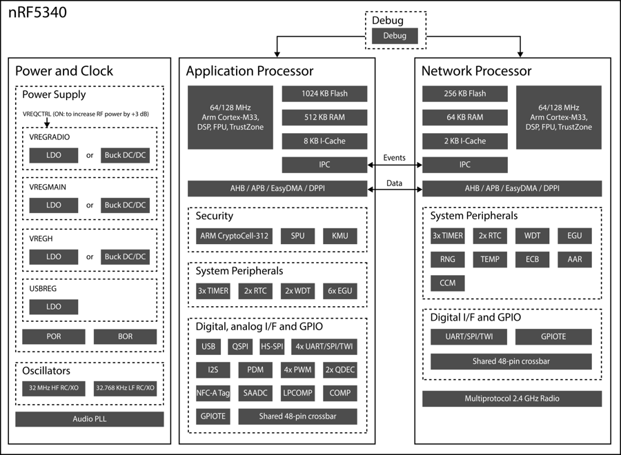
Figure: nRF5340 SoC SW block diagram (adapted from Nordic)
nRF5340 SoC (block diagram nRF5340 SoC SW block diagram (adapted from Nordic)) contains two processors:
Applications Core (high performance)
- Arm Cortex-M33 with DSP (Digital Signal Processing) and FPU (Floating Point Unit), TrustZone support, 1024 kB Flash, 512 kB RAM, 8 kB 2-way set associative cache (serves both internal and external memory), 128 MHz and 64 MHz clock speed, fully programmable and optimized for performance and uses voltage and clock frequency scaling.
- Security (nRF5340 SoC SW block diagram (adapted from Nordic))
- System Peripherals (nRF5340 SoC SW block diagram (adapted from Nordic))
- Digital, analog interfaces and GPIO (nRF5340 SoC SW block diagram (adapted from Nordic))
Network Core (ultra-low power)
- Arm Cortex-M33, 256 kB Flash, 64 kB RAM, 2 kB instructions cache, 64 MHz clock speed, fully programmable and optimized for efficiency
- System Peripherals (nRF5340 SoC SW block diagram (adapted from Nordic))
- Digital interfaces and GPIO (nRF5340 SoC SW block diagram (adapted from Nordic))
- Radio (nRF5340 SoC SW block diagram (adapted from Nordic))
Programming & Firmware
Programmability
BL5340 Default Firmware
The BL5340 module is shipped from Ezurio manufacturing facilities with no firmware loaded.
BL5340 Firmware options
Firmware for use with the BL5340 can be divided into three types.
Bootloader – This is the application that resides on the Application Core used to perform firmware updates of the Application and Network Cores.
The MCUboot [A] or the Trusted Firmware M [B] Bootloaders can be used as the basis for BL5340 Bootloader functionality.
Application – This is the main application code that resides on the Application Core. It interfaces with the Network Core and provides supplementary functionality to that of the time critical activities being performed on the Network Core.
The BL5340 is supported by the Zephyr RTOS [C] and the Nordic Connect SDK [D].
Radio Stack – This is the protocol stack that resides on the Network Core. It controls the radio and performs time critical protocol related operations and provides the results of these to the Application Core for high level processing.
When the Zephyr RTOS is used as the basis for application development, BLE [E] and Thread [F] Radio Stacks are available for use with that platform.
For Nordic Connect SDK based solutions, proprietary BLE [G], Thread [H], Zigbee [I] and ESB [J] protocol stacks are available.
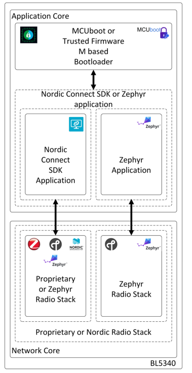
Figure: Functional SW block diagram for BL5340 series BLE module
[A] https://github.com/mcu-tools/mcuboot
[B] https://www.trustedfirmware.org/
[C] https://zephyrproject.org/
[D] https://www.nordicsemi.com/Software-and-tools/Software/nRF-Connect-SDK
[E] https://docs.zephyrproject.org/latest/guides/bluetooth/index.html
[F] https://openthread.io/platforms/rtos/zephyr
[H] https://developer.nordicsemi.com/nRF_Connect_SDK/doc/latest/nrf/ug_thread.html
[I] https://developer.nordicsemi.com/nRF_Connect_SDK/doc/latest/nrf/ug_zigbee.html
[J] https://developer.nordicsemi.com/nRF_Connect_SDK/doc/latest/nrf/ug_esb.html
Interfaces
To provide the widest scope for integration, a variety of physical host interfaces/sensors are provided. The major BL5340 series module functional blocks are described below (which are within the nRF5340). Peripherals not mentioned in this section can be looked up in the nRF5340 datasheet https://infocenter.nordicsemi.com/topic/ps_nrf5340/keyfeatures_html5.html?cp=3_0_0
UART
UARTE – Universal asynchronous receiver/transmitter with Easy DMA
The nRF5340 has 4 UARTs (with flow control CTS, RTS) on the Application Core and 1 UART (with flow control CTS, RTS) On the Network Core. Can be brought out on any GPIO pins. UARTE features:
- Full duplex operation
- Automatic hardware flow control
- Optional even parity bit checking and generation
- Easy DMA (for reading and writing to and from RAM)
- Upto 1Mbps baud rate. Baud rate accuracy depends on HFCLK source selected.
- Return to IDLE between transactions supported (when using HW flow control)
- One or two stop bits
- Least significant bit (LSB) first
- UART’s can be brought out on any GPIOs and independently configurable.
The signaling levels are nominal 0 V and 3.3 V (tracks VDD) and are inverted with respect to the signaling on an RS232 cable.
Two-way hardware flow control is implemented by UART_RTS and UART_CTS. UART_RTS is an output and UART_CTS is an input. Both are active low.
These signals operate according to normal industry convention. UART_RX, UART_TX, UART_CTS, UART_RTS are all 3.3 V level logic (tracks VDD). For example, when RX and TX are idle, they sit at 3.3 V (tracks VDD). Conversely for handshaking pins CTS, RTS at 0 V is treated as an assertion.
The module communicates with the customer application using the following signals:
- Port/TxD of the application sends data to the module’s UART_RX signal line
- Port/RxD of the application receives data from the module’s UART_TX signal line
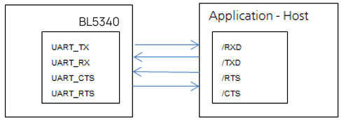
Figure: UART signals
Note: The BL5340 serial module output is at CMOS logic levels (tracks VDD). Level convertor must be added to interface with an RS-232 level compliant interface.
Some serial implementations link CTS and RTS to remove the need for handshaking. We do not recommend linking CTS and RTS other than for testing and prototyping. If these pins are linked and the host sends data at the point that the BL5340 deasserts its RTS signal, there is significant risk that internal receive buffers will overflow, which could lead to an internal processor crash. This will drop the connection and may require a power cycle to reset the module. We recommend you adhere to the correct CTS/RTS handshaking protocol for proper operation.
Table: GPIO used on DVK-BL5340 to bring out UART0 and UART1 interfaces
| Signal Name | Pin No | I/O | Comments |
|---|---|---|---|
| P0.20 / UART0_TX | 14 | O | P0.20 (alternative function UART0_TX) is an output, set high (in firmware). Application Core. |
| P0.22 / UART0_RX | 12 | I | GPIO_08 (alternative function UART0_RX) is an input, set with internal pull-up (in firmware). Application Core. |
| P0.19 / UART0_RTS | 15 | O | P0.19 (alternative function UART0_RTS) is an output, set low (in firmware). Application Core. |
| P0.21 / UART0_CTS | 11 | I | P0.21 (alternative function UART0_CTS) is an input, set with internal pull-down (in firmware). Application Core. |
| P1.08 / UART1_TX | 7 | O | P1.08 (alternative function UART1_TX) is an output, set high (in firmware). Network Core. |
| P1.10 / UART1_RX | 57 | I | P1.10 (alternative function UART1_RX) is an input, set with internal pull-up (in firmware). Network Core. |
| P1.07 / UART1_RTS | 8 | O | P1.07 (alternative function UART1_RTS) is an output, set low (in firmware). Network Core. |
| P1.09 / UART1_CTS | 5 | I | P1.09 (alternative function UART1_CTS) is an input, set with internal pull-down (in firmware). Network Core. |
The GPIO pins in GPIO used on DVK-BL5340 to bring out UART0 and UART1 interfaces are used for UART0 and UART1 interface as assigned for DVK-BL5340 devboard. UART’s can be brought out on any GPIO pin on BL5340 module.
Baud rate accuracy depends on HFCLK source selected.
High baud rates may require GPIOs to be set as High Drive.
USB
USB D – Universal Serial Bus device
BL5340 has USB2.0 FS (Full Speed, 12Mbps) hardware capability.
Table: USB interface
| Signal Name | Pin No | I/O | Comments |
|---|---|---|---|
| D- | 42 | I/O | |
| D+ | 36 | I/O | |
| VBUS | 40 | To use the BL5340 USB peripheral:
When using the BL5340 USB peripheral, the VBUS pin can be supplied from same source as VDD_HV (within the operating voltage range of the VBUS pin and VDD_HV pin). An optional series 4.7Ohms resistor on the USB supply (VBUS) can be fitted for improved immunity to transient over-voltage VBUS connection. If not using USB peripheral, the VBUS pin can be left unconnected. |
SPI
SPI Master – Serial Peripheral Interface master
The nRF5340 supports 4 x SPI master/slave interface (SPIM /SPIS) with easy DMA (on Application Core) and 1 x SPIM master/slave with easy DMA (on Network Core). For this any GPIO pin can be used.
The nRF5340 supports 1 x High Speed SPI master/slave interface (SPIM4) for the fastest SPIM mode (32Mbps) on the Application Core (when running at 128MHz), For SPIM4, dedicated GPIO pins must be used (see High Speed SPI (SPIM4 32Mbps) interface dedicated pins). SMPIM supports Easy DMA direct transfer to and from RAM.
The SPIM interface enables full duplex synchronous communication between devices. It supports a 3-wire (SPI_MOSI, SPI_MISO, SPI_SCK,) bidirectional bus with fast data transfers to and from multiple slaves and optional D/CX output line for distinguishing between command and data bytes. Individual chip select signals are necessary for each of the slave devices attached to a bus, but control of these is left to the application.
The SPI peripheral supports SPI mode 0, 1, 2, and 3.
Table: High Speed SPI (SPIM4 32Mbps) interface dedicated pins
| Signal Name | Pin No | I/O | Comments |
|---|---|---|---|
| P0.08/SPIM4_SCK | 27 | O | These dedicated GPIO pins must be used for 32Mbps high speed SPI using SPIM4, and drive strength configuration H0H1 must be used. Optional D/CX output line for distinguishing between command and data bytes. The D/CX line is set low during transmission of command bytes and high during transmission of data bytes. |
| P0.09/SPIM4_MOSI | 25 | O | |
| P0.10/SPIM4_MISO | 22 | I | |
| P0.11/SPIM4_CSN | 23 | O | |
| P0.12SPIM4_DCX | 20 | O |
SPI Master (SPIM) maximum bit rate is 16Mbps and this may require GPIO to be set as High Drive strength. Other SPIM bit rates are 8Mbps, 4Mbps, 2Mbps, 1Mbps, 500kbps, 250kbps, 125kbps (and accuracy depends on HFCLK source selected).
High Speed SPIM (SPIM4) is 32Mbps and requires to dedicated GPIO pins (Application core when running at 128MHz). For other lower speed SPI, any GPIO pins can be used.
To secure correct behavior in the pins used by SPIM must be configured in the GPIO peripheral before enabling the SPI slave.
SPI Slave – Serial Peripheral Interface slave
The nRF5340 supports 4 x SPI master/slave interface (SPIM /SPIS) with easy DMA (on Application Core) and 1 x SPIM master/slave with easy DMA (on Network Core). For this any GPIO pin can be used.
SPI slave (SPIS) is implemented for ultra-low power communication from an external SPI master. Easy DMA in conjunction with hardware-based semaphore mechanism removes all real time requirements associated with controlling SPI slave from a low priority CPU execution context.
Maximum SPIS bit rate is 8Mbps and the actual maximum data rate depends on the masters CLK to MISO setup and hold timings. Also, this higher SPIS bit rate requires GPIO to be set as High Drive strength.
The MISO line is set in high impedance as long as the SPI slave is not selected with CSN.
To secure correct behavior in the salve SPI slave, the pins used by the SPI slave must be configured in the GPIO peripheral before enabling the SPI slave.
QSPI – Quad Serial Peripheral interface
The nRF5340 supports 1 x QSPI interface peripheral (on Application Core) for communicating with external flash memory device. The main features for QSPI peripheral are:-
- Single/dual/quad SPI input/output
- 6 to 96MHz configurable clock frequency
- Single-word read/write access from/to external flash
- Easy DMA for block read and write transfers
- Up to 48MB/sec Easy DMA read rate
- Execute in place (SIP) for executing program directly from external flash
- XIP (Execute in Place) access can be optional be disabled
- On-the-fly encryption and decryption including Easy DMA and XIP
For QSPI only the dedicated GPIO pins from QSPI Interface dedicated pins shall be used.
Table: QSPI Interface dedicated pins
| Signal Name | Pin No | I/O | Comments |
|---|---|---|---|
| P0.13/QSPI_IO0 | 24 | IO | For QSPI only these dedicated GPIO pins must be used. The GPIO must use the high drive H0H1 (High 0 High 1) configuration. H0H1 is to do with slew rate. |
| P0.14/QSPI_IO1 | 62 | IO | |
| P0.15/QSPI_IO2 | 18 | IO | |
| P0.16/QSPI_IO3 | 17 | IO | |
| P0.17/QSPI_CLK | 16 | O | |
| P0.18/QSPI_CSN | 61 | O |
For all high-speed signal, the printed circuit board (PCB) layout must ensure that connections are made using short PCB traces.
I2C
TWIM – I2C compatible 2-wire interface master
The nRF5340 supports 4 x TWI peripheral (on Application Core and 1 x TWI (on Network Core). The TWI master with Easy DMA (TWIM) is two wire half duplex master which can communicate with multiple slave devices to same bus. Main features of TWIM:
- I2C compatible
- Supported baud rates: 100, 250, 400 and 1000kbps. High bit rates or stronger pull-ups may require GPIOs set as High drive.
- High Speed TWI (1Mbps) is available on dedicated GPIO pins only)
- Support for clock stretching (non I2C compliant)
- EasyDMA
An I2C interface allows multiple masters and slaves to communicate over a shared wired-AND type bus consisting of two lines which normally sit at VDD. The SCL is the clock line which is always sourced by the master and SDA is a bi-directional data line which can be driven by any device on the bus. The protocol makes it possible to interconnect up to 127 individually addressable devices. TWIM is not compatible with CBUS.
IMPORTANT: It is essential to remember that pull-up resistors on both SCL and SDA lines are required. The value of the nRF5340 pull up resistor is 13K Ohms typical. For other values, fit external pull-up resistor on both SCL and SDA as per I2C specification to set speed. The I2C specification allows a line capacitance of 400pF.
Table: High speed TWIM (1Mbps) interface dedicated GPIO pins for proper operation
| Signal Name | Pin No | I/O | Comments |
|---|---|---|---|
| P1.02/I2C_SDA | 37 | I/O | For the fastest TWI 1Mbps mode, the two dedicated high speed TWI pins must be configured and the 20mA open drain driver enabled using the E0E1 drive configuration. For the dedicated, high-speed TWIM pins on P1.02 and P1.03, the E0E1 drive configuration activates a powerful 20 mA open-drain driver specifically designed for high-speed TWI. |
| P1.03/I2C_SCL | 38 | I/O |
The GPIOs used for each two-wire interface can be chosen from any GPIO device and are independently configurable. This enables great flexibility in device pinout and efficient use of Printed Circuit Board space and signal routing.
To secure correct signal levels on the pins used for TWIM while is System OFF mode and when TWIM is disabled, the pins must be configured as in GPIO configuration before entering peripheral TWIM or TWIS.
Table: GPIO configuration before entering peripheral TWIM or TWIS
| Signal Name | Pin No | I/O | Output value | Drive strength |
|---|---|---|---|---|
| I2C_SDA | As specified in PSEL.SCL | I | Not applicable | S0D1 (Standard 0 Disconnect 1) |
| I2C_SCL | As specified in PSEL.SDA | I | Not applicable | S0D1 (Standard 0 Disconnect 1) |
TWIS – I2C compatible 2-wire interface master
TWI slave with EasyDMA (TWIS) is a two-wire half-duplex slave which can communicate with a master device connected to the same bus. Main features for TWIS:
- I2C compatible
- Supported baud rates: 100 and 400 kbps
- EasyDMA
To ensure lowest possible power consumption when the peripheral is not needed stop and disable TWIS.
NFC
NFC Tag – Near field communication tag
The NFCT peripheral is an implementation of an NFC Forum listening device NFC-A. With appropriate software, the NFCT peripheral can be used as the listening device NFC-A as specified by the https://nfc-forum.org/
NFC support:
Based on the NFC forum specification
- 13.56 MHz
- Data rate - 106 kbps
- NFC Type2 and Type4 tag emulation
Modes of operation:
- Disable
- Sense (Wake-on-field low power field detection (SENSE) mode)
- Activated
Use Cases
- Touch-to Pair with NFC
- Launch a smartphone app (on Android)
- NFC enabled Out-of-Band Pairing
System Wake-On-Field function
- Proximity Detection
Table: NFC interface
| Signal Name | Pin No | I/O | Comments |
|---|---|---|---|
| NFC1/P0.02 | 28 | I/O | The NFC pins are by default NFC pins and an alternate function on each pin is GPIO. |
| NFC2/P0.03 | 26 | I/O |
NFC Antenna Coil Tuning Capacitors
From Nordic’s nRF5340 datasheet: https://infocenter.nordicsemi.com/topic/ps_nrf5340/keyfeatures_html5.html?cp=3_0_0
The NFC antenna coil must be the connected differential between the NFC1 and NFC2 pins of the BL5340. Two external capacitors should be used to tune the resonance of the antenna circuit to 13.56 MHz (NFC antenna coil tuning capacitors).
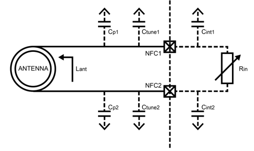
Figure: NFC antenna coil tuning capacitors
The required external tuning capacitor value is given by the following equations:

An antenna inductance of Lant = 0.72 uH provides tuning capacitors in the range of 300 pF on each pin. The total capacitance on NFC1 and NFC2 must be matched. Cint and Cp are small usually (Cint is 4pF), so can omit from calculation.
Battery Protection Note: If the NFC coil antenna is exposed to a strong NFC field, the supply current may flow in the opposite direction due to parasitic diodes and ESD structures.
If the used battery does not tolerate a return current, a series diode must be placed between the battery and the BL5340 to protect the battery.
For more details, see the NFC flexi PCB antenna (Ezurio 0600-0061) datasheet:
https://www.ezurio.com/documentation/datasheet-nfc-flex-pcb-antenna
GPIO
GPIO – General Purpose Input /Output
The 48 general purpose input /output pins (GPIO) are grouped as 2 ports, P0 port has 32 GPIOs and P1 port has 16 GPIOs. They can be accessed individually. Each has the following user configured features:
- Input/output direction
- Output drive strength (standard drive 0.5 mA or high drive 3mA, 5mA)
- Internal pull-up and pull-down resistors (13 K typical) or no pull-up/down or input buffer disconnect
- Wake-up from high or low-level triggers on all pins including NFC pins (Low power detection of pin state changes is possible when in System ON or System OFF)
- Trigger interrupt on state change on any pin (rising edge, falling edge, any change)
Note: When a pin is configured as digital input, care has been taken to minimize increased current consumption when the input voltage is between VIL and VIH. However, it is a good practice to ensure that the external circuitry does not drive that pin to levels between VIL and VIH for a long period of time.
ADC
SAADC – Successive approximation analog-to-digital convertor
The nRF5340 has differential successive approximation register analog to digital convertor (SAADC). Main features of SAADC:
- SAADC on Application Core
- 8/10/12-bit resolution and 14-bit resolution with oversampling
Multiple analog inputs:
- AIN0 to AIN7 pins
- VDD pin
- VDDHDIV5 (through VDDH pin)
8 input channels:
- One channel per singled ended input and two channels per differential input
- Scan mode can be configured with both single ended channels and differential channels
- Each channel can be configured to select any of the above analog inputs
- Full scale input range (0 to VDD)
- Sampling triggered via a task from software or a PPI channel for full flexibility on sample frequency source from low power 32.768kHz RTC or more accurate 1/16MHz timers
- One-shot conversion mode to sample a single channel
- Scan mode to sample a series of channels in sequence with configurable sample delay
- Support for direct sample transfer to RAM using Easy DMA
- Interrupts on single sample and full buffer events
- Sample stored as 16-bit two’s compliment values for differential and single ended sampling
- Continuous sampling without the need of an external timer
- Internal resistor string
- On-the-fly limit checking
The ADC can coexist with COMP and other peripherals using one of the AIN0-AIN7 provided these are assigned to different pins. It is not recommended to select the same analog input for both modules.
BL5340 provides access to 8-channel 8/10/12-bit successive approximation ADC in one-shot mode. This enables sampling up to 8 external signals through a front-end MUX. The ADC has configurable input and reference pre-scaling and sample resolution (8, 10, and 12 bit).
Table: Analog interface on dedicated pins
| Signal Name | Pin No | I/O | Comments |
|---|---|---|---|
| P0.04/AIN0 – Analog Input | 63 | I | This interface is an alternate function on each pin, configurable. Configurable 8, 10, 12-bit resolution. 14-bit resolution with oversampling Eight 8/10/12-bit channels on AIN0-AIN7 or VDD or VDDH/5 Configurable pre-scaling of 4, 2, 1, 1/2, 1/3, 1/4, 1/5 1/6 Configurable acquisition time 3uS, 5uS, 10uS, 15uS, 20uS, 40uS. One-shot mode or Burst mode Scan mode for multiple channels Single ended or Differential or not connected |
| P0.05/AIN1 – Analog Input | 46 | I | |
| P0.06/AIN2 – Analog Input | 64 | I | |
| P0.07/AIN3 – Analog Input | 65 | I | |
| P0.25/AIN4 – Analog Input | 6 | I | |
| P0.26/AIN5 – Analog Input | 2 | I | |
| P0.27AIN6 – Analog Input | 4 | I | |
| P0.28/AIN7 – Analog Input | 53 | I |
PWM
PWM – Pulse Width Modulation
The pulse width modulation (PWM) module allows the generation of PWM signals on GPIO. The module implements an up or up and-and-down counter with 4 x PWM channels (on Application Core) that drive assigned 4 x GPIOs. There are 4 x PWM units with Easy DMA.
PWM features include:
Programmable PWM frequency
- Prescalar of PWM_CLK: divide by 1(16MHz), divide by 2(8MHz), divide by 4(4MHz), divide by 8(2MHz), divide by 16(1MHz), divide by 32(500kHz), divide by 64(250kHz), divide by 128(125kHz)
- Up to four PWM channels with individual polarity and duty cycle values
- Edge or center-aligned pulses across PWN channels
- Multiple duty cycle arrays (sequences) defined in RAM
- Autonomous and glitch-free update of duty cycle values directly from memory through Easy DMA (no CPU involvement)
- Change of polarity, duty cycle and base frequency possibly on every PWM period
- RAM sequences can be repeated or connected into loops.
The PWM output signal has a frequency and duty cycle property. Frequency is adjustable (up to 16 MHz) and the duty cycle can be set over a range from 0% to 100%.
There is a trade-off between PWM output frequency and resolution.
For example:
- PWM output frequency of 500 kHz (2 uS) results in resolution of 1:2.
- PWM output frequency of 100 kHz (10 uS) results in resolution of 1:10.
- PWM output frequency of 10 kHz (100 uS) results in resolution of 1:100.
- PWM output frequency of 1 kHz (1000 uS) results in resolution of 1:1000.
nRESET Pin
Table: nRESET pin
| Signal Name | Pin No | I/O | Comments |
|---|---|---|---|
| nRESET | 54 | I | BL5340 HW reset (active low). The reset pin must be held low (for 0.2uS TBC) to generate a valid reset. Reset time when using pin reset, depending on pin capacitance. 500nF capacitance on reset pin: 13mS (Typ), 40mS (max), 10uF capacitance on reset pin: 260mS (Typ), 800mS (max), e.g., approximately t=5RC where R is the internal pullup 13K Ohms typical enabled. |
A reset in the system is triggered by either a system level or core level reset source. A system level reset will reset all cores. Examples of system level reset are Power-on reset, brownout reset and pin reset. Examples of core level reset are soft reset or lockup will reset either entire core or only part of it. Refer to the nRF5340 datasheet for more details https://infocenter.nordicsemi.com/topic/ps_nrf5340/keyfeatures_html5.html?cp=3_0_0
Temperature Sensor
TEMP – Temperature sensor
TEMP sensor in the Network Core.
Main features of TEMP are:
- Temperature range is greater than or equal to operating temperature range of nRF5340 device
- Resolution is 0.25°C degrees
- The on-silicon temperature sensor accuracy is ±5°C (for TEMP sensor range -20°C to +70°C)
- The on-silicon temperature sensor accuracy is ±7°C (for TEMP sensor range -40°C to +105°C)
- To achieve the measurement accuracy stated, the crystal oscillator must be selected as the HFCLK source
- When the temperature measurement is completed, TEMP analog electronics power down to save power
- TEMP only supports one-shot operation, meaning that every TEMP measurement must be explicitly started
- Time required for temperature measurement 36us typical
- Linearity compensation can be implemented if required by the application
Security and Privacy
Security/Privacy
nRF5340 contains Arm TrustZone CryptoCell™ -312 security subsystem on the Application Core:
- NIST 800-90B, AIS-31, and FIPS 140-2 compliant random number generator
- AES-128 and 256: ECB, CBC, CMAC/CBC-MAC, CTR, CCM/CCM*, GCM
- SHA-1, SHA-2 up to 256 bits
- Keyed-hash message authentication code (HMAC)
- RSA public key cryptography with up to 3072-bit key size
- ECC support for most used curves
- Application key management using derived key model
RADIO – 2.4GHz radio (RF)
2402–2480 MHz Bluetooth Low Energy (BLE) BT5.2 radio transceiver
- -98 dBm RX sensitivity 1 Mbps BLE
- -95 dBm RX sensitivity 2 Mbps BLE
- -104 dBm RX sensitivity 125 kbps BLE coded PHY (s=8)
- -100 dBm RX sensitivity 500 kbps BLE coded PHY (s=2)
- RF Tx output power of +0 dBm programmable down to -1 dBm, -2 dBm, -3 dBm, -4 dBm, -5 dBm, -6 dBm, -7 dBm,
-8 dBm, -12 dBm, -16 dBm, -20 dBm, -40 dBm - RF TX power (for all RF TX power steps) increases by +3 dB when VREQCTRL is turned ON
- Angle of Arrival (AoA) and Angle of Departure (AoD) direction finding using BLE
2405–2480 MHz IEEE 802.15.5-2006 radio transceiver, implementing IEEE 802.15.5-2006 compliant
- 250 kbps, 2450 MHz, O-QPSK PHY
- Channels 11-26. Channel 11 2405 MHz and CH26 2480 MHz
- Clear channel assessment (CCA)
- Energy detection (ED) scan
- CRC generation
- -101 dBm RX sensitivity IEEE 802.15.4-2006 250 kbps
- RF Tx output power of +0 dBm programmable down to -1 dBm, -2 dBm, -3 dBm, -4 dBm, -5 dBm, -6 dBm, -7 dBm,
-8 dBm, -12 dBm, -16 dBm, -20 dBm, -40 dBm. - RF TX power (for all RF TX power steps) increases by +3 dB when VREQCTRL is turned ON.
- MANDATORY. When used in IEEE 802.15.4-2006 PHY mode, channel 26 (2480 MHz), the BL5340 RF TX power must be limited by customer to -8 dBm setting (which produces -5dBm with VREQCTRL ON) maximum RF transmit power to pass FCC/IC Band Edge emissions limit. All other 802.15.4 channels (11-25) may be used up to the maximum 0dBm (which produces +3 dBm with VREQCTRL ON) RF TX output power.
2402–2480 MHz proprietary 1 Mbps and 2 Mbps modes radio transceiver (not currently certified by Ezurio)
- -95 dBm RX sensitivity, 1 Mbps nRF proprietary mode (ideal transmitter)
- -92 dBm RX sensitivity, 2 Mbps nRF proprietary mode (ideal transmitter)
- RF Tx output power of +0 dBm programmable down to -1 dBm, -2 dBm, -3 dBm, -4 dBm, -5 dBm, -6 dBm, -7 dBm,
-8 dBm, -12 dBm, -16 dBm, -20 dBm, -40 dBm. - RF TX power (for all RF TX power steps) increases by +3 dB when VREQCTRL is turned on.
RF interface available in the following two ways:
- 453-00052: RF connected to Integrated PCB trace antenna
453-00053: RF connected to RF Trace Pad
- Antenna options: External dipole antennas connected with to IPEX MH4 RF connector host board
Received Signal Strength Indicator (RSSI)
- RSSI accuracy (valid range -90 to -20dBm) is ±2dB typical
- RSSI resolution 1dB typical
COMP – Comparator
The comparator (COMP) compares an input voltage (VIN+) against a second input voltage (VIN-). VIN+ can be derived from an analog input pin (AIN0-AIN7). VIN- can be derived from multiple sources depending on the operation mode of the comparator.
COMP features include:
- Input range from 0V to VDD
Single-ended mode
- Fully flexible hysteresis using 64-levelo reference ladder
Differential mode
- Configurable hysteresis
Reference input (VREF)
- VDD
- External reference from AIN0 to AIN7 (between 0V t0 VDD)
Three speed/power consumption modes:
- Low power
- Normal
- High speed
- Singe pin capacitive sensor support
- Event generation on output changes
LPCOMP – Low power comparator
Low Power comparator (LPCOMP) compares an input voltage against reference voltage.
LCOMP features include:
- 0V – VDD input range
- Ultra low power
- Eight input options (AIN0 to AIN7)
Reference voltage options:
- Two external analog reference inputs, or
- 15-level internal reference ladder (VDD/16)
- Optional hysteresis-enable on input
- Can be used as a wakeup source from SYSTEM OFF mode
RNG – Random number generator
The Network Core has 1 x Random Number Generator (RNG) that generates true non-deterministic random numbers based on internal thermal noise that are suitable for cryptographic purposes. The RNG does not require a seed value.
I2S – Inter-IC sound interface
The I2S (Inter-IC-Sound Interface) module supports the original two channel I2S format and left or right aligned formats. It implements EasyDMA for sample transfer directly to and from RAM without CPU intervention.
The I2S peripheral main features include:
- Master and Salve mode
- Simultaneous bidirectional (TX and RX) audio streaming
- Original I2S and left or right aligned format
- 32, 24, 16, 8-bit sample width
- Separate sample and word widths
- Low-jitter master clock generator
- Various sample rates
The MCK, SCK, LRCK, SDIN and SDOUT signals associated with the I2S module are mapped to GPIO pins selected when the I2S module is enabled. When a pin is acquired by the I2S module, the direction of the pin (input or output) will be configured automatically and any pin direction setting done in the GPIO module will be overwritten, The directions for the I2S pins is shown in I2S Master interface signals before enabling peripheral and I2S Slave interface signals before enabling peripheral below.
To secure correct signal levels on the pins in System OFF mode and when I2S module is disabled, these pins must be configured in the GPIO peripheral directly.
Table: I2S Master interface signals before enabling peripheral
| Signal Name | Pin No | I/O | Output value | Comments |
|---|---|---|---|---|
| MCK | Any GPIO | O | 0 | I2S master |
| LRCK | Any GPIO | O | 0 | |
| SCK | Any GPIO | O | 0 | |
| SDIN | Any GPIO | I | Not applicable | |
| SDOUT | Any GPIO | O | 0 |
Table: I2S Slave interface signals before enabling peripheral
| Signal Name | Pin No | I/O | Output value | Comments |
|---|---|---|---|---|
| MCK | Any GPIO | O | 0 | I2S slave |
| LRCK | Any GPIO | I | Not applicable | |
| SCK | Any GPIO | I | Not applicable | |
| SDIN | Any GPIO | I | Not applicable | |
| SDOUT | Any GPIO | O | 0 |
PDM – Pulse Density Modulation interface and digital microphones
The pulse density modulation (PDM) module enables input of PDM signals from external audio frontends, such as digital microphones. The PDM peripheral generates the PDM clock and supports single or dual channel (left and right) data input. Data is transferred directly to RAM buffers using EasyDMA.
The PDM peripheral main features include:
- Up to two PDM microphones configured as left/right pair using the same data input
- 16 kHz output sample rate, 16-bit samples
- EasyDMA support for sample buffering
- HW decimation filters
- Selectable ratio of 64 or 80 between PDM_CLK and output sample rate
Table: PDM interface signals
| Signal Name | Pin No | I/O | Comments |
|---|---|---|---|
| DIN | Any GPIO | I | In Application Core |
| CLK | Any GPIO | O |
PDM can be configured with a single microphone (mono), or with two microphones. When a single microphone is used, connect the microphone clock to CLK, and data to DIN.
If two microphones are used, one of them has to be set as left, the other as right (L/R pin tied high or to GND on the respective microphone). It is strongly recommended to use two microphones of exactly the same brand and type so that their timings in left and right operation match.
To ensure correct operation in the PDM module, the pins used by PDM module must be configured in the GPIO peripheral before enabling the PDM module. This is to ensure that the pins used by the PDM module are driven correctly if the PDM module itself is temporarily disabled or the device temporarily enters System OFF. This configuration must be retained in the GPIO for the selected I/O’s as long as the PDM module is supposed to be connected to an external PDM circuit. Only one peripheral can be assigned to drive a particular GPIO pin at a time. Failing to do so may result in unpredictable behavior.
QDEC – Quadrature decoder
The Quadrature decoded (QDEC) provides buffered decoding of quadrature encoded sensor signals. It is suitable for mechanical and optical sensors. QDEC is a 3-pin interface to the off-module quadrature encoder. There are 2 x QDEC in the Application Core.
The QDEC main features include:
- Sample period and accumulation are configurable to match application requirements
- Decoding of digital waveform from off-chip quadrature encoder
- Sample accumulation eliminating hard real time requirements to be enforced on application
- Optional input debounce filters
- Optional LED output signal for optical encoders
To secure correct behavior in the QDEC the pins used by the QDEC must be configured in the GPIO peripheral as shown in QDEC interface signals before enabling peripheral before enabling the QDEC. Only one peripheral can be assigned to drive a particular GPIO pin at a time. Failing to do so may result in unpredictable behavior.
Table: QDEC interface signals before enabling peripheral
| Signal Name | Pin No | I/O | Output Value | Comments |
|---|---|---|---|---|
| Phase A | Any GPIO | I | Not applicable | |
| Phase B | Any GPIO | I | Not applicable | |
| LED | Any GPIO | I | Not applicable |
SWD – Two-wire interface
It is mandatory for the customer to wire out the BL5340 SWD two-wire serial interface on host design for purposes of programming firmware and debug. See SWD BL5340 development board schematic, where the following four lines should be wired out: SWDIO, SWDCLK, GND and VDD).
SWO (P0.11) is a Trace output (called SWO, Serial Wire Output) and is not necessary for programming BL5340 over the SWD interface.
nRESET_BLE is necessary for programming BL5340 over the SWD interface.
Table: Signals for Firmware and Debug
| Signal Name | Pin No | I/O | Comments |
|---|---|---|---|
| SWDIO | 55 | I/O | Internal pull-up resistor (13K) |
| SWDCLK | 56 | I | Internal pull-down resistor (13K) |
| nRESET | 54 | I | Internal pull-up resistor (13K) |
| GND | |||
| VDD |
The Ezurio development board incorporates an on-board USB-to SWD J-link programmer for this purpose.
The SWD connector MPN is as follows:
Table: SWD Connector MPN
| Reference | Part | Description and MPN (Manufacturers Part Number) |
|---|---|---|
| P1 | FTSH-105 | Header, 1.27mm, SMD, 10-way, FTSH-105-01-L-DV Samtech |
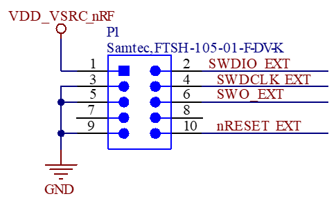
Figure: SWD BL5340 development board schematic
Clocks and Timers
Clocks
HFXO - 32MHz crystal oscillator and nRF53 internal load capacitor 13.5pF mandatory setting
The BL5340 module contains the 32 MHz crystal, but the load capacitors to create 32MHz crystal oscillator circuit are inside the nRF5340 chipset. Customer MUST set the internal nRF5340 capacitors to 13.5pF (for proper operation of the 32 MHz crystal circuit).
The 32 MHz crystal inside the BL5340 module is a high accuracy crystal (±15 ppm at room temperature) that helps with radio operation and reducing power consumption in the active modes.
LFCLK – Low Frequency clock source
There are four possibilities (see nRF5340 SoC clocks (adapted from Nordic)) for the low frequency clock (LFCLK) and options are:
LFRC (32.768kHz RC oscillator): The Internal 32.768 kHz RC oscillator (LFRC) is fully embedded in nRF5340 (and does not require additional external components) with an accuracy ±250 ppm (after calibration of LFRC at least every eight seconds using the HFXO as a reference oscillator). See section LFXO - OPTIONAL 32.768kHz Crystal and Load Capacitor.
LFXO (32.768kHz crystal oscillator): For higher LFCLK accuracy (greater than ±250ppm accuracy is required), the low frequency crystal oscillator (LFXO) must be used. To use LFXO, a 32.768kHz crystal must be connected between the XL1 and XL2 pins and the load capacitance between each crustal terminal and ground. Optionally internal (to nRF53) capacitors of 6pF, 7pF and 9pF are provided on pins XL1 and XL2. See section LFXO - OPTIONAL 32.768kHz Crystal and Load Capacitor.
Low frequency (32.768 kHz) external source: The 32.768 kHz oscillator (LFXO) is designed to work with external sources. Following external sources are supported:
A low swing clock. The signal should be applied to the XL1 pin with XL2 pin grounded.
- In "external low-swing mode" the clock signal can either be a sinewave or a square wave, but it's not allowed to be rail-to-rail. The signal is passed through the LFXO module for amplification and conversion into a digital clock. The amplifier requires a peak-to-peak input amplitude of between 200mV and 1000mV; too high or low amplitude may affect the integrity of the clock. The DC offset of the external signal is flexible, but it must not be so high that XL1 peaks above VDD, or so low that XL1 dips below VSS.
A rail-to-rail clock. The signal should be applied to the XL1 pin with XL2 pin left unconnected.
- In "external full-swing mode" the LFXO is in reality disabled and the XL1 pin configured as a digital input. Hence, the external clock signal must be a digital waveform, with 'high' and 'low' levels as specified in the GPIO chapter. The full-swing mode will consume slightly less current since the internal signal amplifier is not needed and thus powered down. In “external full-swing mode” the XL2 pin is not connected to anything internally but advise to ground any unused pins.
See LFXO - OPTIONAL 32.768kHz Crystal and Load Capacitor in the last row of Optional external 32.768 kHz crystal specification and Low frequency (32.768kHz) external source specification.
LFSYNTH (32.768kHz Synthesised clock) from HFCLK (LFSYNTH): The LFCLK can be synthesised from the HFCLK source. LFSYNTH depends on the HFCLK to run. The accuracy of the LFCLK clock with LFSYNTH as a source assumes the accuracy of the HFCLK. If high accuracy is required, the HFCLK must generated from the HFXO. Using the LFSYNT clock removes the requirement for an external 32.768kHz crystal but the increases the average power consumption as the HFCLK will turned on in the system.
LFXO - OPTIONAL 32.768kHz Crystal and Load Capacitor
This is not required for normal BL5340 module operation.
The nRF5340 on-chip 32.768 kHz LFRC oscillator (±250 ppm) provides protocol timing and helps with radio power consumption in the System ON Idle and System OFF modes by reducing the time that the RX window needs to be open.
To maintain accuracy of the nRF5340 on-chip 32.768 kHz LFRC oscillator within ±250 ppm (which is needed to run the BLE stack), LFRC oscillator needs to be calibrated (which takes 32 mS) regularly. The calibration interval is at least eight seconds which is enough to keep within ±250 ppm.
You can connect an optional external high accuracy (±20 ppm) 32.768 kHz crystal (and associated load capacitors can be external capacitors or use capacitance inside the nRF5340 chipset, which are configurable to either 6pF, 7pF, or 9pF) to the BL5340 P0.01/XL2 (pin 32) and P0.00/XL1 (pin 34). This provides improved protocol timing and to help with radio power consumption in the System ON Idle or System OFF sleep modes by reducing the time that the RX window needs to be open. Comparing current consumption difference between BL5340 on-chip LFRC 32.768 kHz oscillator and optional external crystal (32.768kHz) based oscillator compares the current consumption difference between RC (LFRC) and crystal oscillator (LXFO).
Table: Comparing current consumption difference between BL5340 on-chip LFRC 32.768 kHz oscillator and optional external crystal (32.768kHz) based oscillator
| BL5340 on-chip 32.768 kHz RC Oscillator (±250 ppm) LFRC | Optional External Higher Accuracy (±20 ppm) 32.768 kHz Crystal-based Oscillator LFXO | |
|---|---|---|
| Current Consumption of 32.768 kHz Block | 1.0 uA | 0.16 uA |
| System ON idle + NET Core 64kB RAM + APP Core 8kB RAM retention +RTC run current + LFRC or LFXO) | 2.6 uA | 2.1 uA |
| Calibration | Calibration required regularly (default eight seconds interval). Calibration takes 32 ms; with DCDC used, the total charge of a calibration event is 12.6 uC. The average current consumed by the calibration depends on the calibration interval and can be calculated using the following formula: CAL_charge/CAL_interval – The lowest calibration interval (0.25 seconds) provides an average current of (DCDC enabled): 12.6uC/0.25s = 50.4uA To get the ±250-ppm accuracy, the BLE stack specification states that a calibration interval of eight seconds is enough. This gives an average calibration current of: 12.6uC/8s = 1.6uA Added to the LFRC run current and System ON Idle base current shown above results in a total average current of: LFRC + CAL = 2.6 + 1.6 = 4.2 uA | Not applicable |
| Total | 4.2 uA | 2.1 uA |
| Summary |
|
|
Results with below test setup:
| ||
Table: Optional external 32.768 kHz crystal specification and Low frequency (32.768kHz) external source specification
| Optional external 32.768kHz crystal | Min | Typ | Max |
|---|---|---|---|
| Crystal Frequency | - | 32.768 kHz | - |
| Frequency tolerance requirement of BLE stack | - | - | ±500 ppm |
| Load Capacitance | - | 7 pF | 9 pF |
| Shunt Capacitance | - | 1 pF | 2 pF |
| Equivalent series resistance | - | 60 kOhm | 90 kOhm |
| Drive level | - | - | 0.5 µW |
| Input capacitance on XL1 and XL2 pads with internal capacitor disabled | - | 4 pF | - |
| Input capacitance on XL1 and XL2 pads with internal capacitor enabled | 6 pF | 7 pF | 9 pF |
| Peak to peak amplitude for external low swing clock. Input signal must not be outside supply rails. The allowable input amplitude range in low-swing mode does not change with VDD. | 200 mV | - | 1000 mV |
Be sure to tune the load capacitors on the board design to optimize frequency accuracy (at room temperature) so it matches that of the same crystal standalone, Drive Level (so crystal operated within safe limits) and oscillation margin (Rneg is at least 3 to 5 times ESR) over the operating temperature range.
Other Internal Clocks
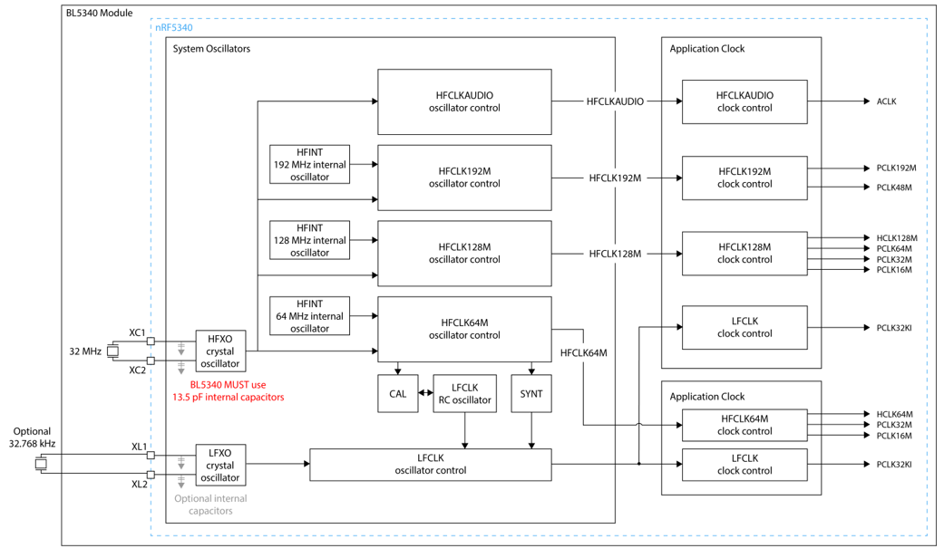
Figure: nRF5340 SoC clocks (adapted from Nordic)
Table: Core clocks
| Core clock | Description |
|---|---|
| HFCLK128M | Scalable 128 MHz CPU clock for the application core |
| HFCLK64M | 64 MHz CPU clock for the network core |
| PCLK192M | Scalable 192 MHz clock for QSPI |
| PCLK64M | 64 MHz peripheral clock |
| PCLK48M | 48 MHz clock for USB |
| PCLK32M | 32 MHz peripheral clock |
| PCLK16M | 16 MHz peripheral clock |
| ACLK | 11.289 MHz or 12.288 MHz tuneable audio peripheral clock |
Timers
TIMER – Timer/counter
There are 3 x 32-bit TIMER peripheral with counter mode (on Application Core and Network Core) and is a general-purpose timer allowing time intervals to be defined by user input. It can operate in two modes (Timer mode and Counter mode).
TIMER runs on HFCLK source and includes 4-bit (1/2X) prescaler that can divide the timer input clock form the HFCLK controller. TIMER base frequency is always 16MHz divided by the prescalar value.
In Timer mode, TIMER’s internal counter register is incremented by one for every tick of the timer frequency fTIMER. The timer frequency is derived from PCLK16M and using value specified in the prescaler register.
fTIMER = 16MHz / (2PRESCALAR)
When fTIMER ≤1MHz, TIMER uses PCLK1M instead of PCLK16M for reduced power consumption.
In Counter mode, the timer frequency and prescaler are not utilized but the TIMER’s internal counter register is incremented by one each time the COUNT Task is triggered.
RTC – Real Timer Counter
There are 2 x 24-bit real timer counter (RTC) on Application Core and 2 x RTC on Network Core. The real time counter (RTC) module provides a generic, low power timer on the low frequency clock source (LFCLK). When started, the RTC will automatically request LFCLK source with RC oscillator if the LFCLK is not already running.
Mandatory SW requirements related to hardware
32MHz crystal internal load capacitor setting of 13.5pF
MANDATORY. BL5340 module contains the 32 MHz crystal but the load capacitors to create 32 MHz crystal oscillator circuit are inside the nRF5340 chipset. Customer MUST set the internal nRF5340 capacitors to 13.5 pF (for proper operation of the 32 MHz crystal circuit in the BL5340 module).
CH26 (2480MHz) IEEE 802.15.4-2006 RF TX power
MANDATORY. When used in IEEE 802.15.4-2006 PHY mode, channel 26 (2480MHz), the BL5340 RF TX power must be limited by customer to -8 dBm setting (which produces -5dBm with VREQCTRL ON) maximum RF transmit power to pass FCC/IC Band Edge emissions limit. All other 802.15.4 channels (11-25) may be used up to the maximum 0dBm (which produces +3 dBm with VREQCTRL ON) RF TX output power.
Hardware Architecture
Block Diagrams
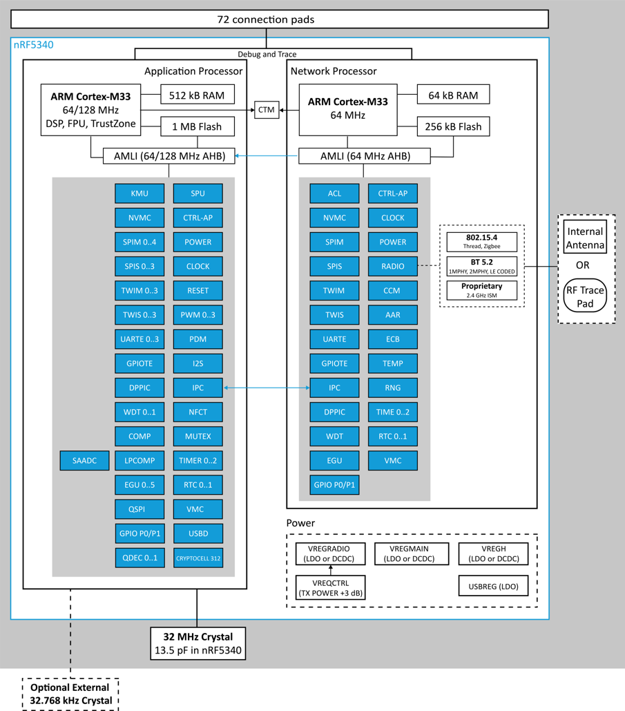
Figure: BL5340 HW block diagram
Pin-Out / Package Layout
Pin Definitions
Table: Pin definitions
| Pin # | Pin Name | nRF5340 QFN Pin | nRF5340 QFN Name | Comment |
|---|---|---|---|---|
| 1 | GND | - | VSS | - |
| 2 | P0.26 / AIN5 | AL29 | P0.26 / AIN5 | Dedicated pin for ADC Ezurio Devkit: Ethernet chip SPI_MISO |
| 3 | P0.24 | AL27 | P0.24 | Ezurio Devkit: INT2_ACC interrupt from 3-axis accelerometer chip |
| 4 | P0.27 / AIN6 | AK30 | P0.27 / AIN6 | Dedicated pin for ADC Ezurio Devkit: Ethernet chip SPI_MOSI |
| 5 | P1.09 | AK26 | P1.09 | Ezurio Devkit: UART1_CTS |
| 6 | P0.25 / AIN4 | AK28 | P0.25 / AIN4 | Dedicated pin for ADC Ezurio Devkit: Ethernet chip SPI_CS |
| 7 | P1.08 | AL23 | P1.08 | Ezurio Devkit: UART1_TX |
| 8 | P1.07 | AK24 | P1.07 | Ezurio Devkit: UART1_RTS |
| 9 | P1.06 | AL21 | P1.06 | Ezurio Devkit: Interrupt from Port Expander chip PE_INT |
| 10 | P1.05 | AK22 | P1.05 | See Note 6 |
| 11 | P0.21 | AL15 | P0.21 | Ezurio Devkit: UART0_CTS |
| 12 | P0.22 | AK18 | P0.22 | Ezurio Devkit: UART0_RX |
| 13 | P1.04 | AL19 | P1.04 | See Note 6 |
| 14 | P0.20 | AK16 | P0.20 | Ezurio Devkit: UART0_TX |
| 15 | P0.19 | AL13 | P0.19 | Ezurio Devkit: UART0_RTS |
| 16 | P0.17 / QSPI_CLK | AK12 | P0.17 / QSPI_CLK | Dedicated pin for QSPI Ezurio Devkit: QSPI flash chip |
| 17 | P0.16 / QSPI_IO3 | AL9 | P0.16 / QSPI_IO3 | Dedicated pin for QSPI Ezurio Devkit: QSPI flash chip |
| 18 | P0.15 / QSPI_IO2 | AK10 | P0.15 / QSPI_IO2 | Dedicated pin for QSPI Ezurio Devkit: QSPI flash chip |
| 19 | GND | - | VSS | - |
| 20 | P0.12 / TRACECLK / SPIM4_DCX | AK6 | P0.12 / TRACECLK / SPIM4_DCX | Dedicated pin for High-speed SPI (SPIM4, 32Mbps) and Trace Ezurio Devkit: LCD assembly SPIM4_DCX |
| 21 | GND | - | VSS | - |
| 22 | P0.10 / TRACEDATA1 / SPIM4_MISO | AK2 | P0.10 / TRACEDATA1 / SPIM4_MISO | Dedicated pin for High-speed SPI (SPIM4, 32Mbps) and Trace Ezurio Devkit: LCD assembly SPIM4_SPI_MISO |
| 23 | P0.11 / TRACEDATA0 / SPIM4_CSN | AK4 | P0.11 / TRACEDATA0 / SPIM4_CSN | Dedicated pin for High-speed SPI (SPIM4, 32Mbps) and Trace. SWO also comes out on P0.11 Ezurio Devkit: LCD assembly SPIM4_CS |
| 24 | P0.13 / QSPI_IO0 | AL5 | P0.13 / QSPI_IO0 | Dedicated pin for QSPI Ezurio Devkit: QSPI flash chip |
| 25 | P0.09 / TRACEDATA2 / SPIM4_MOSI | AJ1 | P0.09 / TRACEDATA2 / SPIM4_MOSI | Dedicated pin for High-speed SPI (SPIM4, 32Mbps) and Trace Ezurio Devkit: LCD assembly SPIM4_MOSI |
| 26 | P0.03 / NFC2 | AA1 | P0.03 / NFC2 | Dedicated pin for NFC Ezurio Devkit: NFC Coil flexi-PCB NFC antenna plug into CON2 |
| 27 | P0.08 / TRACEDATA3 / SPIM4_SCK | AH2 | P0.08 / TRACEDATA3 / SPIM4_SCK | Dedicated pin for High-speed SPI (SPIM4, 32Mbps) and Trace Ezurio Devkit: LCD assembly SPIM4_SCL |
| 28 | P0.02 / NFC1 | W1 | P0.02 / NFC1 | Dedicated pin for NFC Ezurio Devkit: NFC Coil flexi-PCB NFC antenna plug into CON2 |
| 29 | GND | - | VSS | - |
| 30 | GND | - | VSS | - |
| 31 | VDD | A19, B8, L1 | VDD | 1.7V to 3.6V |
| 32 | P0.01 / XL2 | R1 | P0.01 / XL2 | Dedicated pin for NFC Ezurio Devkit: Optional 32.768kHz crystal pad XL2 and associated 7pF load capacitor inside nRF5340 chipset. |
| 33 | GND | - | VSS | |
| 34 | P0.00 / XL1 | N1 | P0.00 / XL1 | Dedicated pin for NFC Ezurio Devkit: Optional 32.768kHz crystal pad XL1 and associated 7pF load capacitor inside nRF5340 chipset. |
| 35 | VDD_HV | E1 | VDD_HV | 2.5V – 5.5V |
| 36 | D+ | B2 | D+ | Ezurio Devkit: USB3 |
| 37 | P1.02 / I2C_SDA | AE1 | P1.02 / I2C_SDA | Dedicated pins for High-speed TWI (1Mbps). Ezurio Devkit: Multiple I2C sensors:- 3-axis Accelerometer chip, LCD assembly, RTC chip, Temp/Pres/HMD sensor chip, DAC chip, Eeprom chip, Port Expander (PE) chip which has 4 LED’s, 4 BUTTONS connected to PE chip. |
| 38 | P1.03 / I2C_SCL | AF2 | P1.03 / I2C_SCL | |
| 39 | GND | - | VSS | - |
| 40 | VBUS | A5 | VBUS | 4.35V – 5.5V |
| 41 | P1.00 | M2 | P1.00 | See Note 6 |
| 42 | D- | B4 | D- | Ezurio Devkit: USB3 |
| 43 | P1.01 | P2 | P1.01 | See Note 6 |
| 44 | GND | - | - | - |
| 45 | P1.15 | B14 | P1.15 | Ezurio Devkit: SD card DO/DAT0 |
| 46 | P0.05 / AIN1 | Y2 | P0.05 / AIN1 | Dedicated pin for ADC Ezurio Devkit: LCD assembly LCD_CTP_INT |
| 47 | P1.13 | A17 | P1.13 | Ezurio Devkit: SD card DI/CMD |
| 48 | P1.14 | B16 | P1.14 | Ezurio Devkit: SD card SCLK/CLK |
| 49 | P1.12 | B18 | P1.12 | Ezurio Devkit: SD card CS_SD/DAT3 |
| 50 | P1.11 | B20 | P1.11 | Ezurio Devkit: BOOT BUTTON (S4) |
| 51 | P0.31 | B22 | P0.31 | See Note 6 |
| 52 | P0.30 | B24 | P0.30 | See Note 6 |
| 53 | P0.28 / AIN7 | AE31 | P0.28 / AIN7 | Dedicated pin for ADC Ezurio Devkit: Ethernet chip SPI_SCK |
| 54 | nRESET | AC31 | nRESET | System Reset (Active Low). Internal 13K pull up inside nRF5340. |
| 55 | SWDIO | AA31 | SWDIO | Pull up resistor (13K) inside nRF5340 |
| 56 | SWDCLK | W31 | SWDCLK | Pull down resistor (13K) inside nRF5340 |
| 57 | P1.10 | R31 | P1.10 | Ezurio Devkit: UART1_RX |
| 58 | P0.29 | U31 | P0.29 | See Note 6 |
| 59 | GND | - | VSS | - |
| 60 | P0.23 | AK20 | P0.23 | Ezurio Devkit: INT1_ACC interrupt from 3-axis accelerometer |
| 61 | P0.18 / QSPI_CSN | AK14 | P0.18 / QSPI_CSN | Dedicated pin for QSPI Ezurio Devkit: QSPI flash chip |
| 62 | P0.14 / QSPI_IO1 | AK8 | P0.14 / QSPI_IO1 | Dedicated pin for QSPI Ezurio Devkit: QSPI flash chip |
| 63 | P0.04 / AIN0 | V2 | P0.04 / AIN0 | Dedicated pin for ADC |
| 64 | P0.06 / AIN2 | AB2 | P0.06 / AIN2 | Dedicated pin for ADC Ezurio Devkit: LCD assembly LCD_Reset |
| 65 | P0.07 / AIN3 | AD2 | P0.07 / AIN3 | Dedicated pin for ADC Ezurio Devkit: Interrupt from Ethernet chip INT_ETH |
| 66 | GND | - | VSS | - |
| 67 | GND | - | VSS | - |
| 68 | GND | - | VSS | - |
| 69 | GND | - | VSS | - |
| 70 | GND | - | VSS | - |
| 71 | GND | - | VSS | - |
| 72 | RF_pad or NC | - | - | RF pad active on BL5340 RF pin variant 453-0053. NC on BL5340 Integrated antenna variant 453-0052 |
| 73 | GND | - | VSS | - |
| 74 | GND | - | VSS | - |
| 75 | GND | - | VSS | - |
| Pin Definition Notes: | |
| Note 1 GPIO | GPIO = General Input or Output (GPIO level voltage tracks VDD pin). AIN =Analog input. If GPIO is selected as an input, ensure the input is not floating (which can cause current consumption to drive with time in low power modes (such as System ON Idle), by selecting the internal pull up or pull down. Must connect all GND pads to host board PCB GND plane. |
| Note 2 QSPI/SPI/TWI/Trace | QSPI, High-Speed SPI (SPIM4) 32 Mbps, TWI 1 Mbps and Trace come on dedicated GPIO pins only. Other lower speed SPI (16 Mbps, 8 Mbps, 4 Mbps, 2 Mbps, 1 Mbps, 500 kbps, 250 kbps, 125 kbps) and TWI (400 kbps, 250 kbps, 100 kbps) can come out on any GPIO pins. |
| Note 3 USB | If using the USB interface, then the BL5340 VBUS pin (pin40) must be connected to external supply within the range 4.35V to 5.5V. When using the BL5340 VBUS pin (pin40), you MUST externally fit a 4.7uF to ground. |
| Note 4 SWDIO / SWCLK / nRESET / VDD / GND | Customer MUST bring out SWDIO, SWCLK, nRESET, VDD, GND for programming purposes. A reset in the system is triggered by either a system level or core level reset source. A system level reset resets all cores. Examples of system level resets – power-on reset, brownout reset, and pin reset. Examples of core level resets – soft reset, lockup (resets either the entire core or only part of it). Refer to the nRF5340 datasheet for more details: https://infocenter.nordicsemi.com/topic/ps_nrf5340/keyfeatures_html5.html?cp=3_0_0 SWD- Two-wire interface |
| Note 5 RF_PAD | RF_pad (pin72) is for the BL5340 RF pad variant (453-00053) module only. If using the BL5340 module RF pad variant (453-00053), customer MUST copy the 50-Ohms GCPW RF track design, MUST add series 2nH RF inductor (Murata LQG15HN2N0B02# or Murata LQG15HS2N0B02) and RF connector IPEX MHF4 Receptacle (MPN: 20449-001E) detailed in section 50-Ohms RF Trace and RF Match Series 2nH RF inductor on Host PCB for BL5340 RF pad variant (453-00053) |
| Note 6 BL5340PA NC GPIO | The 8 GPIOs signals P0.04/AIN0, P0.29, P0.30, P0.31, P1.00, P1.01, P1.04, P1.05 are NC pins on BL5340PA module series. |
Mechanical Drawings
BL5340 Mechanical Details
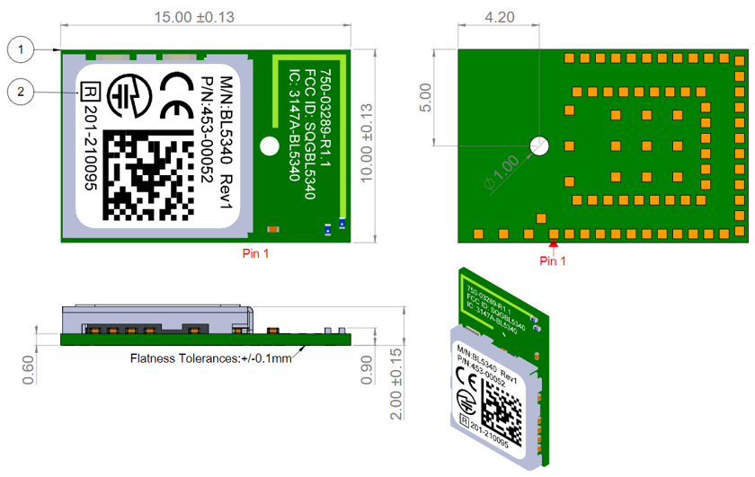
Figure: Mechanical Details - Chip Antenna
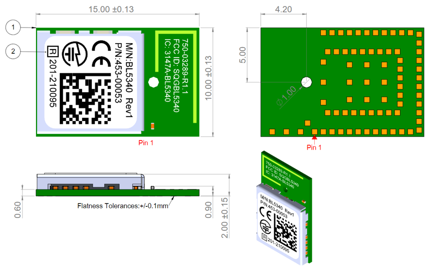
Figure: Mechanical Details - Trace Pin
3D models for External Antenna Trace Pin and Internal Antenna, SCH symbols (Altium format), PCB footprints (DXF and Altium format) and Development Kit Schematics can be found on the BL5340 product page – http://ezurio.com/bl5340-series
Schematics
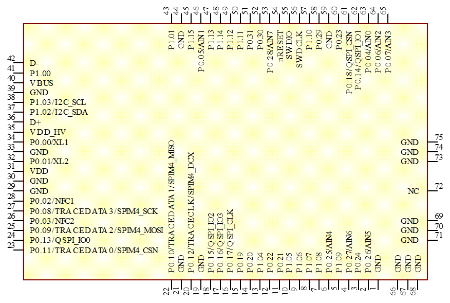
Figure: Top view - Schematic symbol for 453-00052 BL5340 Multi-Core/Protocol -Bluetooth +802.15.4+NFC Module (Nordic nRF5340) - Integrated Antenna
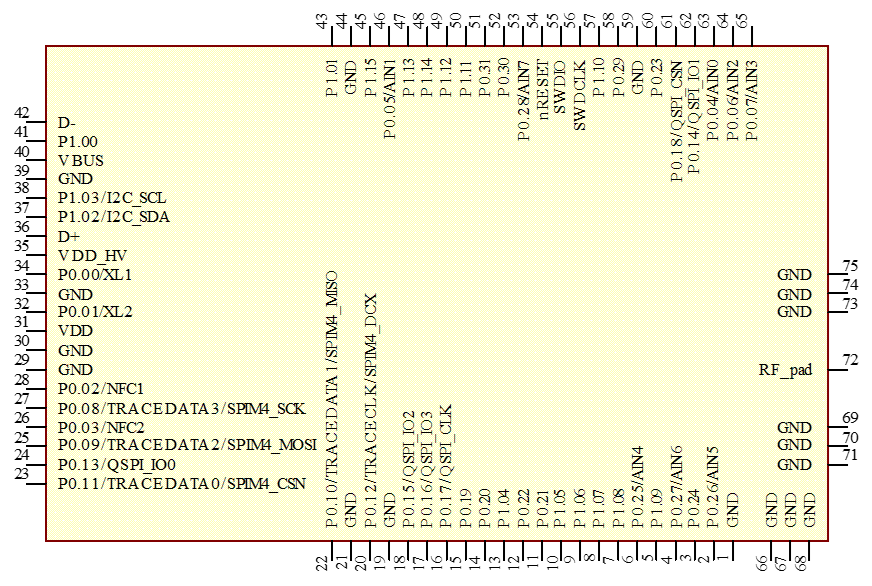
Figure: Top view - Schematic symbol for 453-00053 BL5340 Multi-Core/Protocol -Bluetooth +802.15.4+NFC Module (Nordic nRF5340) -Trace pin
Electrical Characteristics
Absolute Maximum Ratings
Absolute maximum ratings are the extreme limits for supply voltage and voltages on digital and analogue pins of the module are listed below; exceeding these values causes permanent damage.
Table: Absolute maximum ratings
| Parameter | Min | Max | Unit |
|---|---|---|---|
| Voltage at VDD pin | -0.3 | +3.9 (Note 1) | V |
| Voltage at VDD_HV pin | -0.3 | +5.8 | V |
| VBUS | -0.3 | +5.8 | V |
| Voltage at GND pin | 0 | V | |
| Voltage at GPIO pin (at VDD≤3.6V) | -0.3 | VDD +0.3 | V |
| Voltage at GPIO pin (at VDD≥3.6V) | -0.3 | 3.9 | V |
| NFC antenna pin current (NFC1/2) | - | TBD | mA |
| Radio RF input level | - | TBD | dBm |
| Environmental | |||
| Storage temperature | -40 | +105 | ºC |
| MSL (Moisture Sensitivity Level) | - | 4 | - |
| ESD (as per EN301-489) Conductive Air Coupling | 4 8 | kV kV | |
| Flash Memory (Endurance) (Note 2) | - | 10000 | Write/erase cycles |
| Flash Memory (Retention) | - | 10 years at 40°C | - |
| Absolute maximum Ratings Notes: | |
| Note 1 | The absolute maximum rating for VDD pin (max) is 3.9V for the BL5340. |
| Note 2 | Wear levelling can be implemented by customer. |
Recommended Operating Conditions
Recommended Operating Parameters
Table: Power supply operating parameters
| Parameter | Min | Typ | Max | Unit |
|---|---|---|---|---|
| VDD (independent of DCDC) supply range | 1.7 | 3.0 | 3.6 | V |
| VDD_HV (independent of DCDC) supply range | 2.5 | 3.7 | 5.5 | V |
| VBUS USB supply range | 4.35 | 5 | 5.5 | V |
| VDD Maximum ripple or noise (See Note 1) | - | - | 10 | mV |
| Time in Power-on reset after supply reaches minimum operating voltage, depend on supply rise time. VDD supply rise time (0V to 1.7V)210uS VDD supply rise time (0V to 1.7V)2>10mS | - - | 0.7 0 | 1.0 - | mS mS |
| Operating Temperature Range | -40 | +25 | +105 | ºC |
| Recommended Operating Parameters Notes: | |
| Note 1 | This is the maximum VDD or VDD_HV ripple or noise (at any frequency) that does not disturb the radio. |
| Note 2 | The on-board power-on reset circuitry may not function properly for rise times longer than the specified maximum. |
| Note 3 | BL5340 power supply options:
For either option, if you use USB interface then the BL5340 VBUS pin must be connected to external supply within the range 4.35V to 5.5V. When using the BL5340 VBUS pin, you MUST externally fit a 4.7uF to ground. |
Table: Signal levels for interface, GPIO
| Parameter | Min | Typ | Max | Unit |
|---|---|---|---|---|
| VIH Input high voltage | 0.7 VDD | VDD | V | |
| VIL Input low voltage | VSS | 0.3 x VDD | V | |
| VOH Output high voltage (std. drive, 0.5mA, VDD≥1.7V) (high-drive, 3mA, VDD≥1.7V) (high-drive, 5mA, VDD≥2.7V) | VDD -0.4 VDD -0.4 VDD -0.4 | VDD VDD VDD | V V V | |
| VOL Output low voltage (std. drive, 0.5mA, VDD≥1.7V) (high-drive, 3mA, VDD≥1.7V) (high-drive, 5mA, VDD≥2.7V) | VSS VSS VSS | VSS+0.4 VSS+0.4 VSS+0.4 | V V V | |
| VOL Current at VSS+0.4V, Output set low (std. drive, VDD≥1.7V) (high-drive, VDD≥1.7V) (high-drive, VDD≥2.7V) QSPI (high-drive, VDD≥1.7V)) TWIM (high-drive, VDD≥1.7V)) | 1 3 6 - - | 2 - - 10 50 | 4 - - - - | mA mA mA mA mA |
| VOH Current at VDD -0.4, Output set high (std. drive, VDD≥1.7V) (high-drive, VDD≥2.7V) (high-drive, VDD≥1.7V) QSPI (high-drive, VDD≥1.7V)) | 1 6 3 - | 2 - - 10 | 3 - - | mA mA mA mA |
| Pull up resistance | 13 | kΩ | ||
| Pull down resistance | 13 | kΩ | ||
| Pad capacitance | 1.5 | pF | ||
| Pad capacitance at NFC pads | 4 | pF | ||
| Leakage current between NFC pads when driven to different states | 1 | 10 | uA |
| Signal Levels Notes: | |
| Note 1 | The GPIO (GPIO) high reference voltage always equals the level on the VDD pin.
|
Table: GPIO pin alternative function AIN (ADC) specification
| Parameter | Min | Typ | Max | Unit |
|---|---|---|---|---|
ADC channels (AIN), single ended (SE) or differential ADC channels (AIN) ADC channels other through VDD pin ADC channels other through VDDH pin | SE or DE AIN0 to AIN7 VDD VDDHDIV5 | |||
| ADC modes (single channel) ADC modes (multiple channel) | One-shot mode or Continuous mode Scan mode | |||
| ADC Internal reference voltage Input range or ADC External VDD as reference voltage Input range | (±0.6)/Gain (±VDD/4)/Gain | V V | ||
| ADC pin input internal selectable scaling gain | 4, 2, 1, 1/2, 1/3, 1/4, 1/5 1/6 | Scaling gain | ||
| ADC input pin (AIN) voltage maximum without damaging ADC w.r.t(see Note 1) VCC Prescaling (Gain) 0V-VDD 4, 2, 1, ½, 1/3, ¼, 1/5, 1/6 | VSS | VDD+0.3 | V | |
| Configurable Resolution Configurable Resolution with oversampling | 8 - | 10 - | 12 14 | bits bits |
| Maximum sampling rate | 200 | kHz | ||
| Configurable (see Note 2) Acquisition Time, source resistance ≤10kΩ Acquisition Time, source resistance ≤40kΩ Acquisition Time, source resistance ≤100kΩ Acquisition Time, source resistance ≤200kΩ Acquisition Time, source resistance ≤400kΩ Acquisition Time, source resistance ≤800kΩ | 3 5 10 15 20 40 | uS uS uS uS uS uS | ||
| Conversion Time(see Note 3) | 2 | uS | ||
| ADC input impedance (during operation) (see Note 3) Input Resistance Sample and hold capacitance at maximum gain | 1 2.5 | MOhm pF |
| Recommended Operating Parameters Notes: | |
| Note 1 | On AIN pin, do not violate ADC maximum input voltage (for damage) for a given VDD, e.g. With internal reference, single ended input (ground negative input) and gain of 1/6, the input range is equal to (0.6V)/(1/6) or 3.6V. If VDD is 3.6V, you can only expose AIN pin to VDD+0.3 V. With reference chosen as VDD, single ended input (ground negative input) and gain of 1/4 the input range is equal to (VDD/4)/(1/4) or VDD. |
| Note 2 | ADC resolution (8-bit, 10-bit, 12-bit, 14bit mode), acquisition time, gain, reference voltage source, single ended or differential input, ADC mode and oversampling (for 14bit mode) are configurable. BL5340 ADC is a Successive Approximation type ADC (SSADC). As a result, no external capacitor is needed for ADC operation. Configure the acquisition time according to the source resistance of external connection to ADC (that customer has). In Continuous mode, the sampling frequency is limited by the sum of sampling time and acquisition time (fsample < 1/(tACQ + tconv)). The maximum sampling time is 2us. For acquisition time of 3us the total conversion time is therefore 5us, which makes maximum sampling frequency of 1/5us = 200kHz. Similarly, if acquisition time of 40us chosen, then the conversion time is 42us and the maximum sampling frequency is 1/42us = 23.8kHz. In scan mode the sample time is the time it takes to sample all channels (Total sample time < Sum(CH[x] x (/(tACQ + tconv)) where x=0..enabled channels. When using VDDHDIV5 as input, the acquisition time needs to be 10uS or higher. |
| Note 3 | ADC input impedance is estimated mean impedance of the ADC (AIN) pins. |
Power Management & Consumption
Power Consumption
Normal voltage mode VDD of 3.0 V, using internal (to chipset) DCDC or with internal (to chipset) LDO ON. Temperature 25ºC.
Table: Power consumption
| Parameter | Typ (Radio only) | Typ Radio +Application core (20kB RAM) + Network core (64kB RAM) | Unit |
|---|---|---|---|
| Active mode ‘peak’ current (Note 1) (Advertising or Connection) | With DCDC [with LDO] | With DCDC [with LDO] | mA |
| Tx only run peak current @ Txpwr = +3 dBm (Note1A) | 5.1 [11.3] | 9.1 [21.5] | mA |
| Tx only run peak current @ Txpwr = 0 dBm | 3.4 [9.1] | 9.1 [20.2] | mA |
| Tx only run peak current @ Txpwr = -4 dBm | 2.7 [7.2] | - | mA |
| Tx only run peak current @ Txpwr = -8 dBm | 2.2 [5.8] | - | mA |
| Tx only run peak current @ Txpwr = -12 dBm | 2.0 [5.0] | - | mA |
| Tx only run peak current @ Txpwr = -16 dBm | 1.8 [4.5] | - | mA |
| Tx only run peak current @ Txpwr = -20 dBm | 1.7 [4.2] | - | mA |
| Tx only run peak current @ Txpwr = -40 dBm | 1.5 [3.8] | - | mA |
| Active Mode | |||
| Rx only ‘peak’ current, BLE 1Mbps (Note 1) | 2.7[6.7] | 8.6 [21.5] | mA |
| Rx only ‘peak’ current, BLE 2Mbps (Note 1) | 3.1 [7.9] | - | mA |
| Ultra-Low Power Mode 1 (Note 2) | |||
| System ON Idle (0 k application, network core RAM retention) | 1.3 | uA | |
| Ultra-Low Power Mode 2 (Note 3) | |||
| System OFF (0 kB application and network RAM retention) | 0.9 | uA | |
| Active Mode Average current (Note 4) | |||
| Advertising Average Current draw | |||
| Max, with advertising interval (min) 20 mS | Note4 | uA | |
| Min, with advertising interval (max) 10240 mS | Note4 | uA | |
| Connection Average Current draw | |||
| Max, with connection interval (min) 7.5 mS | Note4 | uA | |
| Min, with connection interval (max) 4000 mS | Note4 | uA | |
| Power Consumption Notes: | |
| Note 1 | This is for Peak Radio Current only (with VREQCTRL OFF). Also, additional current draw depending on Application Core and Network Core running, RAM, flash used and which peripherals on (if any). Note1A: With VREQCTRL ON (get +3 dB extra RF TX power), the Peak Radio current increases by |
| Note 2 | BL5340 modules System ON Idle is 1.3 uA typical (with 0kB application core RAM, wake on any event, network core RAM 0kB, network core forced off). System ON Idle is entered automatically (waiting for an event). In System ON Idle, all peripherals that are enabled stay on and may re-awaken the chip. Depending on active peripherals, current consumption ranges from 1.3 μA to 645 uA (when UART is ON, Idle). See individual peripherals current consumption data in the Peripheral Block Current Consumption section. There is functionality to detect GPIO change with no current consumption cost, it is possible to close the UART and get to the 1.3 uA current consumption regime and still be able to detect for incoming data and be woken up so that the UART can be re-opened at expense of losing that first character. RAM retention current per 4k block is approximately 13nA. |
| Note 3 | In System OF (0kB application RAM, wake on reset, network core RAM 0kB), everything is disabled, and the only wake-up sources (including NFC to wakeup) are reset and changes on GPIO or NFC pins on which sense is enabled. The current consumption seen is ~0.9 uA typical in BL5340 modules.
|
| Note 4 | Average current consumption depends on several factors (including Tx power, VDD, accuracy of 32MHz and 32.768 kHz). With these factors fixed, the largest variable is the advertising or connection interval set. Advertising Interval range:
For an advertising event:
Other factors that are also related to average current consumption include the advertising payload bytes in each advertising packet and whether it’s continuously advertising or periodically advertising. Connection Interval range (for a peripheral):
For a connection event (for a peripheral device):
Other factors that are also related to average current consumption include:
Connection Interval range (for a central device):
|
Peripheral Block Power Consumption
Peripheral Block Current Consumption
The values below are calculated for a typical operating voltage of 3V (Normal voltage mode).
Table: Common conditions of 3V operating voltage
| Condition | Value | Note |
|---|---|---|
| Supply | 3V on VDD/VDD_HV(Normal voltage mode) | |
| Temperature | 25°C | |
| CPU | (WFI(wait for interrupt)/WFE(wait for event) sleep | |
| Peripherals | All idle | |
| Clock | HFCLK = HFINT @64MHz, LFCLK=not running | |
| Regulator | DCDC ON for VREGMAIN, VREGRADIO and VREGH (when used) | |
| Application core RAM | 8kB | In System ON, RAM value refers to the amount of RAM that is switched on. The remainder of RAM is non retained. In System OFF, RAM value refers to amount of RAM that is retained. |
| Application core RAM | 0kB | |
| Cache enabled | Yes | Only applies when the CPU is running from flash memory. |
| Network core Forced off | yes | |
| 32MHz crystal | yes | Only applies when the high frequency crystal oscillator (HFXO) is running. HFXO is used when the radio is running |
| 32.768kHz crystal | yes | Only applies when the low frequency crystal oscillator (LFXO) is running. |
Table: UART power consumption
| Parameter | Min | Typ | Max | Unit | |
|---|---|---|---|---|---|
| WITH DCDC | WITH LDO | ||||
| UARTE RX idle (started, waiting for data, no data transfer) | - | 645 | - | - | uA |
| UARTE RX idle (started, waiting for data, no data transfer), clock=HFXO64M | - | 840 | - | - | uA |
| UART transferring data @ 1200 bps clock=HFXO64M | - | 885 | - | - | uA |
| UART transferring data @ 115200 bps clock=HFXO64M | - | 890 | - | - | uA |
| UART receiving data @ 115200 bps clock=HFXO64M | - | 890 | - | - | uA |
| UART transmitting and receiving data @ 115200 bps clock=HFXO64M | - | 895 | - | - | uA |
| UART Baud rate | 1 | - | 1000 | kbps | |
Table: SPIM and SPIS power consumption
| Parameter | Min | Typ | Max | Unit | |
|---|---|---|---|---|---|
| WITH DCDC | WITH LDO | ||||
| SPI Master transferring data @ 2 Mbps | - | 935 | - | - | uA |
| SPI Master transferring data @ 2 Mbps, clock=HFXO64M | - | 1145 | - | - | uA |
| SPI Master transferring data @ 8 Mbps | - | 1705 | - | - | uA |
| SPI Master transferring data @ 8 Mbps, clock=HFXO64M | - | 1930 | - | - | uA |
| SPI Master transferring data @ 32 Mbps | - | 2115 | - | - | uA |
| SPI Master transferring data @ 32 Mbps, clock=HFXO64M | - | 2345 | - | - | uA |
| SPIS configured and idle (enabled, no CSN activity) | - | 145 | - | - | uA |
| SPIS transferring data @ 2Mbps | - | 713 | - | - | uA |
| SPIS transferring data @ 2 Mbps, clock=HFXO64M | 913 | - | - | uA | |
Table: TWIM and TWIS (I2C) power consumption
| Parameter | Min | Typ | Max | Unit | |
|---|---|---|---|---|---|
| WITH DCDC | WITH LDO | ||||
| TWIM transferring data @100kbps | - | 965 | - | - | uA |
| TWIM transferring data @100kbps, clock=HFXO64M | - | 1170 | - | - | uA |
| TWIM transferring data @400kbps | - | 1000 | - | - | uA |
| TWIM transferring data @400kbps, clock=HFXO64M | - | 1250 | - | - | uA |
| TWIM transferring data @1000kbps | - | 2050 | - | - | uA |
| TWIM transferring data @1000kbps, clock=HFXO64M | - | 2295 | - | - | uA |
| TWIS configured and enabled (IDLE state) | - | 45 | - | - | uA |
| TWIS transferring data @100kbps | - | 945 | - | - | uA |
| TWIS transferring data @400kbps | - | 985 | - | - | uA |
| TWIS transferring data @100kbps, clock=HFXO64M | - | 1150 | - | - | uA |
| TWIS transferring data @400kbps, clock=HFXO64M | - | 1185 | - | - | uA |
Table: ADC power consumption
| Parameter | Min | Typ | Max | Unit | |
|---|---|---|---|---|---|
| WITH DCDC | WITH LDO | ||||
ADC current during conversion SAADC sampling @16ksps, acquisition time =20uS, clock HFXO | - | 980 | - | - | uA |
| SAADC sampling @1kHz from RTC intask mode, LPOP=Lowlat, acquisition time =20uS, clock HFINT64M and LFXO | - | 770 | - | - | uA |
| SAADC sampling @1kHz from RTC in task mode, LPOP=LowPower, acquisition time =20uS, clock HFINT64M and LFXO | - | 160 | - | - | uA |
Table: COMP and LCOMP power consumption
| Parameter | Min | Typ | Max | Unit | |
|---|---|---|---|---|---|
| WITH DCDC | WITH LDO | ||||
| COMP enabled, Low power mode | - | 60 | - | - | uA |
| COMP enabled, normal power mode | - | 62 | - | - | uA |
| COMP enabled, High power mode | - | 68 | - | - | uA |
| LCOMP enabled | - | 45 | - | - | uA |
Table: QSPI power consumption
| Parameter | Min | Typ | Max | Unit | |
|---|---|---|---|---|---|
| WITH DCDC | WITH LDO | ||||
| QSPI idle (enabled, but not activated) | - | 45 | - | - | uA |
| QSPI active (activated, but not transferring data) | - | 1790 | - | - | uA |
| QSPI active (activated and transferring data to /from external flash memory), SCKFREQ=96MHz, quad mode, clock=HFXO192M | - | 4430 | - | - | uA |
Table: NFC power consumption
| Parameter | Min | Typ | Max | Unit | |
|---|---|---|---|---|---|
| WITH DCDC | WITH LDO | ||||
| System ON, current in SENSE STATE (this current does not apply when in NFC field) | - | 1.3 | - | - | uA |
| System ON, current in ACTIVATED STATE, clock=HFXO64M | - | 1080 | - | - | uA |
Table: PWM power consumption
| Parameter | Min | Typ | Max | Unit | |
|---|---|---|---|---|---|
| WITH DCDC | WITH LDO | ||||
| PWM running at 125kHz, top=10, duty=50% | - | 560 | - | - | uA |
| PWM running at 16MHz, top=10, duty=50% | - | 560 | 1035 | - | uA |
| PWM running at 125kHz, top=10, duty=50%, clock=HFXO64M | - | 750 | - | - | uA |
| PWM running at 16MHz, top=10, duty=50%, clock=HFXO64M | - | 755 | - | - | uA |
Table: TIMER power consumption
| Parameter | Min | Typ | Max | Unit | |
|---|---|---|---|---|---|
| WITH DCDC | WITH LDO | ||||
| One TIMER running @1MHz | - | 475 | - | - | uA |
| One TIMER running @1MHz, clock=HFXO64M | - | 670 | - | - | uA |
| One TIMER running @16MHz | - | 560 | 1040 | - | uA |
| One TIMER running @16MHz, clock=HFXO64M | - | 750 | 1280 | - | uA |
| One TIMER running @16MHz, clock=HFINT28M | - | 750 | - | - | uA |
| One network TIMER running @1MHz | - | 170 | - | - | uA |
| One network TIMER running @1MHz, clock=HFXO64M | - | 400 | - | - | uA |
| One network TIMER running @16MHz | - | 220 | - | - | uA |
Table: WDT power consumption
| Parameter | Min | Typ | Max | Unit | |
|---|---|---|---|---|---|
| WITH DCDC | WITH LDO | ||||
| Application MCU WDT started | - | 2.0 | 4.9 | - | uA |
| Network MCU started, 64kB network RAM | - | 3.2 | - | - | uA |
Table: TEMP Power Consumption
| Parameter | Min | Typ | Max | Unit | |
|---|---|---|---|---|---|
| WITH DCDC | WITH LDO | ||||
| TEMP started, 64kB network RAM | - | 615 | - | - | uA |
Table: RNG power consumption
| Parameter | Min | Typ | Max | Unit | |
|---|---|---|---|---|---|
| WITH DCDC | WITH LDO | ||||
| RNG running, 64kB network RAM | - | 270 | - | - | uA |
Table: QDEC power consumption
| Parameter | Min | Typ | Max | Unit | |
|---|---|---|---|---|---|
| WITH DCDC | WITH LDO | ||||
| QDEC running | - | 460 | - | - | uA |
Table: PDM power consumption
| Parameter | Min | Typ | Max | Unit | |
|---|---|---|---|---|---|
| WITH DCDC | WITH LDO | ||||
| PDM receiving and processing data @1Msps (RATIO=64, PDMCLKCTRL=135274496), stereo mode, clock=HFXO64M | - | 655 | - | - | uA |
| PDM receiving and processing data @1Msps (RATIO=64, PDMCLKCTRL=3435997056), stereo mode, clock=HFXO64M | - | 1045 | - | - | uA |
Table: I2S power consumption
| Parameter | Min | Typ | Max | Unit | |
|---|---|---|---|---|---|
| WITH DCDC | WITH LDO | ||||
| I2S transferring data @ 2x16bitx16kHz (CONFIG.MCKFREQ=32MDIV63, CONFIG.RATIO=32X), clock=HFXO64M | - | 2000 | - | - | uA |
| I2S transferring data @ 2x16bitx16kHz (CONFIG.MCKFREQ=510000, CONFIG.RATIO=32X), clock=HFXO ACLK@12.288MHz | - | 2170 | - | - | uA |
| I2S transferring data @ 2x16bitx48kHz (CONFIG.MCKFREQ=505286656, CONFIG.RATIO=32X), clock=HFXO ACLK@12.288MHz | - | 2310 | - | - | uA |
Table: USB active power consumption
| Parameter | Min | Typ | Max | Unit | |
|---|---|---|---|---|---|
| WITH DCDC | WITH LDO | ||||
| Current from VBUS supply, USB active | - | 1.2 | - | - | uA |
| Current from VBUS supply, USB suspended, CPU sleeping | - | 180 | - | - | uA |
| Current from VDD supply (normal voltage mode), all RAM retained, CPU running, USB active | - | 3.0 | - | - | uA |
| Current from VDD supply (normal voltage mode), all RAM retained, CPU running, USB suspended | - | 815 | - | - | uA |
| Current from VDD supply (normal voltage mode), all RAM retained, CPU sleeping, USB suspended, regulator = LDO | - | 135 | - | - | uA |
| Current from VDDH supply (high voltage mode), VDD=3 V (VREGH output), all RAM retained, CPU running, USB active | - | 3.2 | - | - | uA |
| Current from VDDH supply (high voltage mode), VDD=3 V (VREGH output), all RAM retained, CPU sleeping, USB suspended | - | 2340 | - | - | uA |
| Current from VDDH supply (high voltage mode), VDD=3 V (VREGH output), all RAM retained, CPU sleeping, USB suspended, regulator = LDO | - | 125 | - | - | uA |
| Current from VDD supply, USB disabled, VBUS supply connected, all RAM retained, CPU sleeping | - | 3 | - | - | uA |
The above current consumption is for the given peripheral including the internal blocks that are needed for that peripheral for both the case when DCDC is on and off. The peripheral Idle current is when the peripheral is enabled but not running (not sending data or being used) and must be added to the System ON Idle current. In all cases radio is not turned on.
For asynchronous interface, like the UART (asynchronous as the other end can communicate at any time), the UART on the BL5340 must be kept open, resulting in the base current consumption penalty.
For a synchronous interface like the I2C or SPI (since BL5340 side is the master), the interface can be closed and opened when needed, resulting in current saving (no base current consumption penalty). There’s a similar argument for ADC (open ADC when needed).
Power Supply Options
BL5340 Power Supply Options
Power management features:
- System ON Idle, System OFF and Force-OFF mode.
- Open/Close peripherals (UART, SPI, QSPI, I2C, GPIOs, ADC, NFC, I2S, PDM etc.). Peripherals consume current when open; each peripheral can be individually closed to save power consumption
- Use of the internal DCDC convertor or LDO
- Supply voltage to be read (through the internal ADC)
- Pin wake-up system from System OFF (including from NFC pins)
Power supply features:
- Supervisor hardware to manage power during reset, brownout, or power fail.
- 1.7V to 3.6V supply range for normal power supply (VDD pin) using internal DCDC convertor or LDO
- 2.5V to 5.5 supply range for High voltage power supply (VDD_HV pin) using internal DCDC convertor or LDO
- 4.35V to 5.5V supply range for powering USB (VBUS pin) portion of BL5340 only. The remainder of the BL5340 module circuitry must still be powered through the VDD (or VDD_HV) pin.
The BL5340 module power supply internally contains the following two main supply regulator stages (BL5340 power supply block diagram (adapted from the following resource: https://infocenter.nordicsemi.com/topic/ps_nrf5340/keyfeatures_html5.html?cp=3_0_0):
- VREGH – Connected to the VDD_HV pin
VREGMAIN and VREGRADIO – Connected to the VDD pin
The USB peripheral is powered separately (connected to the VBUS pin).
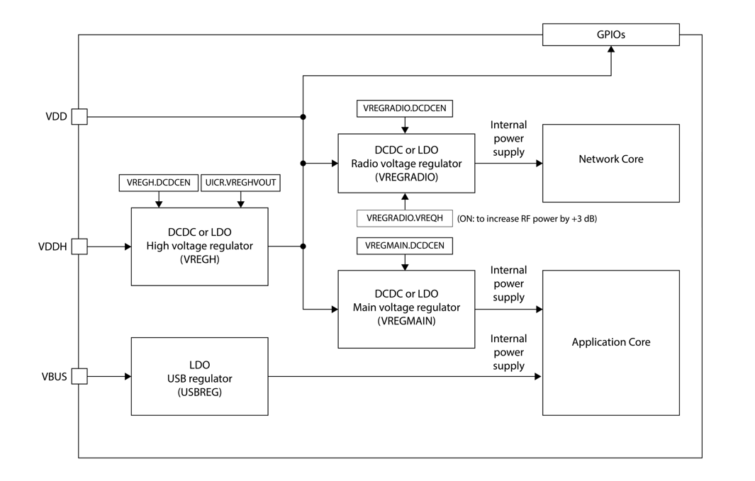
Figure: BL5340 power supply block diagram (adapted from the following resource: https://infocenter.nordicsemi.com/topic/ps_nrf5340/keyfeatures_html5.html?cp=3_0_0
Normal Voltage mode (option1) or High Voltage mode (option2)
The BL5340 power supply system enters one of two supply voltage modes, Normal or High voltage mode, depending on how the external supply voltage is connected to these pins.
BL5340 power supply options:
- Option 1 – Normal voltage power supply mode entered when the external supply voltage is connected to both the VDD and VDD_HV pins (so that VDD equals VDD_HV). Connect external supply within range 1.7V to 3.6V range to BL5340 VDD and VDD_HV pins.
OR
- Option 2 – High voltage mode power supply mode (using BL5340 VDD_HV pin) entered when the external supply voltage in ONLY connected to the VDD_HV pin and the VDD pin is not connected to any external voltage supply. Connect external supply within range 2.5V to 5.5V range to BL5340 VDD_HV pin. BL5340 VDD pin left unconnected.
For either option, if you use USB interface then the BL5340 VBUS pin must be connected to external supply within the range 4.35V to 5.5V. When using the BL5340 VBUS pin, you MUST externally fit a 4.7uF to ground.
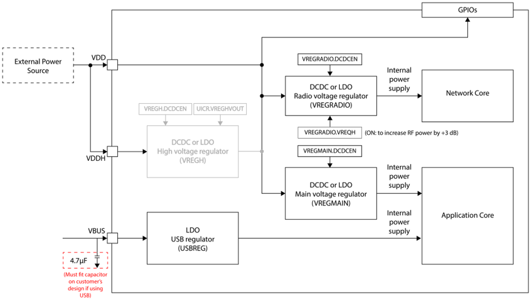
Figure: Normal Voltage mode (option1)
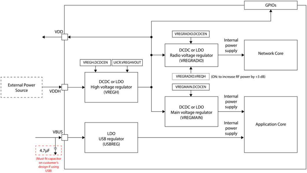
Figure: High Voltage Mode (option2)
BL5340 powering options summarizes these power supply options.
Table: BL5340 powering options
| Power Supply Pins and Operating Voltage Range | OPTION 1: Normal voltage mode. Module pins to connect external supply. | OPTION 2: High voltage mode. Module pins to connect external supply. | OPTION 1 with USB peripheral, and Normal voltage mode. Module pins to connect external supply. | OPTION 2 with USB peripheral and high voltage mode. Module pins to connect external supply. |
|---|---|---|---|---|
| VDD (pin31) 1.7V to 3.6V | Yes | No | Yes | No (See Section VBUS pin and 4.7uF Mandatory Capacitor) |
| VDD_HV (pin35) 2.5V to 5.5V | No | Yes | No | Yes (See Section VBUS pin and 4.7uF Mandatory Capacitor) |
| VBUS (pin40) 4.35V to 5.5V | No | (See Note 3) | Yes (See Section VBUS pin and 4.7uF Mandatory Capacitor) | Yes (See Section VBUS pin and 4.7uF Mandatory Capacitor) |
| Power Supply Option Notes: | |
|---|---|
| Note 1 | Option 1 – External supply voltage is connected to BOTH the VDD and VDD_HV pins (so that VDD equals VDD_HV). Connect external supply within range 1.7V to 3.6V range to BOTH BL5340 VDD and VDD_HV pins. |
| Note 2 | Option 2 – External supply within range 2.5V to 5.5V range to the BL5340 VDD_HV pin ONLY. BL5340 VDD pin left unconnected. In High voltage mode, the VDD pin becomes an output voltage pin. It can be used to supply external circuitry from the VDD pin. Before any current can be taken from the BL5340 VDD pin, this feature must be enabled in the BL5340. Additionally, the VDD output voltage is configurable from 1.8V to 3.3V with possible settings of 1.8V, 2.1V, 2.4V, 2.7V, 3.0V, and 3.3V. The default voltage is 1.8V. The supported BL5340 VDD pin output voltage range depends on the supply voltage provided on the BL5340 VDD_HV pin. The minimum difference between voltage supplied on the VDD_HV pin and the voltage output on the VDD pin is 0.3 V. The maximum output voltage of the VDD pin is VDDH – 0.3V. Current that can be drawn by external circuitry from VDD pin in High voltage mode (supply on VDD_HV) shows the current that can be drawn by external circuitry from VDD pin in high voltage mode (supply on VDD_HV). |
Table: Current that can be drawn by external circuitry from VDD pin in High voltage mode (supply on VDD_HV)
| Parameter | Min | Typ | Max | Unit |
|---|---|---|---|---|
| External current draw (from VDD pin) allowed in High Voltage mode (supply on VDD_HV) during System OFF (BL5340 System OFF) | 1 | mA | ||
| External current draw (from VDD pin) NOTE3A allowed in High Voltage mode (supply on VDD_HV) when VREGMAIN and VREGRADIO are in DCDC mode. Assumes worst case power consumption for both cores (NOTE3B) and at the lowest VDD output voltage setting. | 7 | mA | ||
| External current draw (from VDD pin) NOTE3A allowed in High Voltage mode (supply on VDD_HV) when VREGMAIN and VREGRADIO are in LDO mode. Assumes worst case power consumption for both cores (NOTE3B) and at the lowest VDD output voltage setting. | 1 | mA | ||
| Minimum difference between voltage supplied on VDD_HV pin and output voltage on VDD pin (configured in VREGHOUT), VDD_HV > VDD | 0.3 | V | ||
| VDD output voltage | 1.8 | 3.3 | V | |
| VDD output voltage error (deviation from setting in) | -10 | +5 | % |
A: External current draw is the sum of all GPIO currents and current being drawn from VDD.
B: In practice, the maximum external current draw is limited by the maximum output current of VREGH, subtracting the actual current being drawn from VDD.
| Note 3 | Depends on whether USB operation is required. See VBUS pin and 4.7uF Mandatory Capacitor if USB peripheral is to be used. |
VBUS pin and 4.7uF Mandatory Capacitor
To use the BL5340 USB peripheral:
- Connect the BL5340 VBUS pin to the external supply within the range 4.35V to 5.5V. When using the BL5340 VBUS pin, you MUST externally fit a 4.7uF to ground. Ensure capacitor value reduction due to DC bias, AC bias, temperature is minimized.
- Connect the external supply to either the VDD (Option 1) or VDD_HV (Option 2) pin to operate the rest of BL5340 module.
When using the BL5340 USB peripheral, the VBUS pin can be supplied from same source as VDD_HV (within the operating voltage range of the VBUS pin and VDD_HV pin).
An optional series 4.7Ohms resistor on the USB supply (VBUS) can be fitted for improved immunity to transient over-voltage VBUS connection.
If not using USB peripheral, the VBUS pin can be left unconnected.
VREQCTRL - Voltage request control (VREQCTRL ON for +3dB extra RF TX power)
The VREQCTRL can request additional voltage on VREGRADIO regulated supply to support an extra +3dB RF TX power out of the radio.
Table: RF TX Power setting versus VREQCTRL OFF and VREQCTRL ON (to get +3dB extra RF TX power)
| nRF5340 RF TX power setting | Register VREQCTRL OFF Actual nRF5340 RF TX power | Register VREQCTRL ON (to add extra +3 dB) Actual nRF5340 RF TX power |
|---|---|---|
| 0 dBm | 0 dBm | +3 dBm (= 0 dBm +3 dB) |
| -1 dBm | -1 dBm | +2 dBm (= -1 dBm +3 dB) |
| -2 dBm | -2 dBm | +1 dBm (= -2 dBm +3 dB) |
| -3 dBm | -3 dBm | 0 dBm (= -3 dBm +3 dB) |
| -4 dBm | -4 dBm | -1 dBm (= -4 dBm +3 dB) |
| -5 dBm | -5 dBm | -2 dBm (= -5 dBm +3 dB) |
| -6 dBm | -6 dBm | -3 dBm (= -6 dBm +3 dB) |
| -7 dBm | -7 dBm | -4 dBm (= -7 dBm +3 dB) |
| -8 dBm | -8 dBm | -5 dBm (= -8 dBm +3 dB) |
| -12 dBm | -12 dBm | -9 dBm (= -12 dBm +3 dB) |
| -16 dBm | -16 dBm | -13 dBm (= -16 dBm +3 dB) |
| -20 dBm | -20 dBm | -17 dBm (= -20 dBm +3 dB) |
| -40 dBm | -40 dBm | -37 dBm (= -40 dBm +3 dB) |
Low Power Modes
The nRF5340 chipset (BL5340 module) has four power modes: Active, System ON Idle, System OFF and Force-OFF mode.
For low power consumption, the module can be placed automatically in System ON Idle if there are no pending events. The module wakes from System ON Idle via any interrupt (such as a received character on the UART Rx line). If the module receives a UART character from either the external UART or the radio, it wakes up.
System OFF is the lowest power mode. Once awakened, the system goes through a system reset.
Force-OFF is only applicable for network core.
Integration Guidelines
Antenna Characteristics
453-00052 On-Board PCB Trace Antenna Characteristics
The 453-00052 on-board PCB trace monopole antenna radiated performance depends on the host PCB layout.
The BL5340 development board was used for BL5340 development and the 453-00052 PCB antenna performance evaluation. To obtain similar performance, follow guidelines in section Host PCB Land Pattern and Antenna Keep-out for the 453-00052 to allow the on-board PCB antenna to radiate and reduce proximity effects due to nearby host PCB GND copper or metal covers.
| Antenna Efficiency | 2402MHz | 2440MHz | 2480MHz | |||
|---|---|---|---|---|---|---|
| Peak | Avg | Peak | Avg | Peak | Avg | |
| 453-00052 PCB trace antenna | +0.2dBi | -4.24dBi | +1.49dBi | -3.19dBi | +1.39dBi | -3.27dBi |
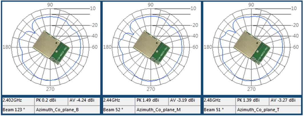
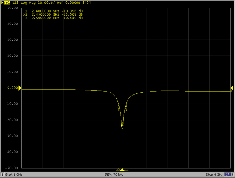
Figure: 453-00052 on-board PCB antenna performance (Antenna Gain and S11 – whilst 453-00052 module sitting on Devboard 453-00052-K1)
Circuit (Overview and Checklist)
The BL5340 is easy to integrate, requiring no external components on your board apart from those which you require for development and in your end application.
The following are suggestions for your design for the best performance and functionality.
Checklist (for Schematic):
- BL5340 power supply options:
Option 1 – Normal voltage power supply mode entered when the external supply voltage is connected to both the VDD and VDDH pins (so that VDD equals VDD_HV). Connect external supply within range 1.7V to 3.6V range to BL5340 VDD and VDD_HV pins.
OR
Option 2 – High voltage mode power supply mode (using BL5340 VDD_HV pin) entered when the external supply voltage in ONLY connected to the VDD_HV pin and the VDD pin is not connected to any external voltage supply. Connect external supply within range 2.5V to 5.5V range to BL5340 VDD_HV pin. BL5340 VDD pin left unconnected.
External power source should be within the operating range, rise time and noise/ripple specification of the BL5340. Add decoupling capacitors for filtering the external source. Power-on reset circuitry within BL5340 series module incorporates brown-out detector, thus simplifying your power supply design. Upon application of power, the internal power-on reset ensures that the module starts correctly.
- BL5340 USB peripheral:
To use the BL5340 USB peripheral:
- Connect the BL5340 VBUS pin to the external supply within the range 4.35V to 5.5V. When using the BL5340 VBUS pin, you MUST externally fit a 4.7uF to ground. Ensure capacitor value reduction due to DC bias, AC bias, temperature is minimized.
- Connect the external supply to either the VDD (Option 1) or VDD_HV (Option 2) pin to operate the rest of BL5340 module.
When using the BL5340 USB peripheral, the VBUS pin can be supplied from same source as VDD_HV (within the operating voltage range of the VBUS pin and VDD_HV pin).
An optional series 4.7Ohms resistor on the USB supply (VBUS) can be fitted for improved immunity to transient over-voltage VBUS connection.
If not using USB peripheral, the VBUS pin can be left unconnected.
- AIN (ADC) and GPIO pin IO voltage levels
BL5340 GPIO voltage levels are at VDD. Ensure input voltage levels into GPIO pins are at VDD also (if VDD source is a battery whose voltage drops). Ensure ADC pin maximum input voltage for damage is not violated. - AIN (ADC) impedance and external voltage divider setup
If you need to measure with ADC a voltage higher than 3.6V, you can connect a high impedance voltage divider to lower the voltage to the ADC input pin. - SWD
This is REQUIRED for loading firmware. MUST wire out the SWD two wire interface on host design (see SWD BL5340 development board schematic). Five lines should be wired out, namely SWDIO, SWDCLK, nRESET, GND and VDD. - UART and flow control (CTS, RTS)
Required if customer requires UART. - TWI (I2C)
It is essential to remember that pull-up resistors on both SCL and SDA lines are required, the value as per I2C standard. nRF5340 can provide 13K Ohms typical pull up values internally. For other values, fit external pull-up resistor on both SCL and SDA as per I2C specification to set speed. The I2C specification allows a line capacitance of 400pF. QSPI, High Speed SPI (SPIM4, 32Mbps), High speed TWI (I2C, 1Mbps), QSPI and Trace
QSPI, High-Speed SPI (SPIM4) 32Mbps, TWI 1Mbps and Trace come on dedicated GPIO pins only. Other lower speed SPI and TWI can come out on any GPIO pins.For all high-speed signal, the printed circuit board (PCB) layout must ensure that connections are made using short PCB traces.
- GPIO pins
If GPIO is selected as an input, ensure the input is not floating (which can cause current consumption to drive with time in low power modes (such as System ON Idle), by selecting the internal pull up or pull down. NFC antenna connector
To make use of the Ezurio flexi-PCB NFC antenna, fit connector:
- Description – FFC/FPC Connector, Right Angle, SMD/90d, Dual Contact,1.2 mm Mated Height
- Manufacturer – Molex
Manufacturers Part number – 512810594
Add tuning capacitors of 300 pF on NFC1 pin to GND and 300 pF on NFC2 pins to GND if the PCB track length is similar as development board.
- nRESET pin (active low)
Hardware reset. Wire out to push button or drive by host.
By default module is out of reset when power applied to VDD pins (13K pull-up inside nRF5340). Optional External 32.768kHz crystal
If the optional external 32.768kHz crystal is needed, then use a crystal that meets specification and add load capacitors (either inside nRF5340 or discrete capacitors outside nRF53) whose values should be tuned to meet all specification for frequency and oscillation margin.
BL5340 module RF pad variant (453-00053)
RF_pad (pin72) is for the BL5340 RF pad variant (453-00053) module only. If using the BL5340 module RF pad variant (453-00053), customer MUST copy the 50-Ohms GCPW RF track design, MUST add series 2nH RF inductor (Murata LQG15HN2N0B02# or Murata LQG15HS2N0B02) and RF connector IPEX MHF4 Receptacle (MPN: 20449-001E) Detailed in the following section:
50-Ohms RF Trace and RF Match Series 2nH RF inductor on Host PCB for BL5340 RF pad variant (453-00053)
PCB Layout
PCB Layout on Host PCB - General
Checklist (for PCB):
- MUST locate BL5340 module close to the edge of PCB (mandatory for the 453-00052 for on-board PCB trace antenna to radiate properly).
- Use solid GND plane on inner layer (for best EMC and RF performance).
- All module GND pins MUST be connected to host PCB GND.
- Place GND vias close to module GND pads as possible.
- Unused PCB area on surface layer can flooded with copper but place GND vias regularly to connect the copper flood to the inner GND plane. If GND flood copper is on the bottom of the module, then connect it with GND vias to the inner GND plane.
- Route traces to avoid noise being picked up on VDD, VDDH, VBUS supply and AIN (analogue), GPIO (digital) traces and high-speed traces.
- Ensure no exposed copper is on the underside of the module (refer to land pattern of BL5340 development board).
Antenna Keep-Out on Host PCB
The 453-00052 has an integrated PCB trace antenna and its performance is sensitive to host PCB. It is critical to locate the 453-00052 on the edge of the host PCB (or corner) to allow the antenna to radiate properly. Refer to guidelines in section PCB land pattern and antenna keep-out area for the 453-00052. Some of those guidelines repeated below.
- Ensure there is no copper in the antenna keep-out area on any layers of the host PCB. Keep all mounting hardware and metal clear of the area to allow proper antenna radiation.
- For best antenna performance, place the 453-00052 module on the edge of the host PCB, preferably in the edge center.
- The BL5340 development board (453-00052-K1) has the 453-00052 module on the edge of the board (not in the corner). The antenna keep-out area is defined by the BL5340 development board which was used for module development and antenna performance evaluation is shown in PCB trace Antenna keep-out area (shown in red), corner of the BL5340 development board for the 453-00052 module., where the antenna keep-out area is ~4.7 mm wide, ~39.17 mm long; with PCB dielectric (no copper) height ~1 mm sitting under the 453-00052 PCB trace antenna.
- The 453-00052 PCB trace antenna is tuned when the 453-00052 is sitting on development board (host PCB) with size of 135 mm x 110 mm x 1mm.
- A different host PCB thickness dielectric will have small effect on antenna.
- The antenna-keep-out defined in the Host PCB Land Pattern and Antenna Keep-out for the 453-00052 section.
- Host PCB land pattern and antenna keep-out for the BL5340 applies when the 453-00052 is placed in the edge of the host PCB preferably in the edge center. PCB trace Antenna keep-out area (shown in red), corner of the BL5340 development board for the 453-00052 module. shows an example.
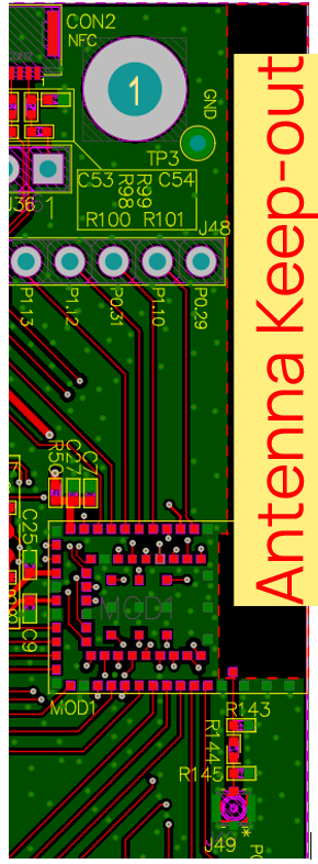
Figure: PCB trace Antenna keep-out area (shown in red), corner of the BL5340 development board for the 453-00052 module.
| Antenna Keep-out Notes: | |
|---|---|
| Note 1 | The BL5340 module is placed on the edge, preferably edge centre of the host PCB. |
| Note 2 | Copper cut-away on all layers in the Antenna Keep-out area under the 453-00052 on host PCB. |
Antenna Keep-out and Proximity to Metal or Plastic
Checklist (for metal /plastic enclosure):
- Minimum safe distance for metals without seriously compromising the antenna (tuning) is 40 mm top/bottom and 30 mm left or right.
- Metal close to the 453-00052 PCB trace monopole antenna (bottom, top, left, right, any direction) will have degradation on the antenna performance. The amount of that degradation is entirely system dependent, meaning you will need to perform some testing with your host application.
- Any metal closer than 20 mm will begin to significantly degrade performance (S11, gain, radiation efficiency).
- It is best that you test the range with a mock-up (or actual prototype) of the product to assess effects of enclosure height (and materials, whether metal or plastic) and host PCB ground (GND plane size).
50-Ohms RF Trace and RF Match Series 2nH RF inductor on Host PCB for BL5340 RF pad variant (453-00053)
To use an external antenna requires BL5340 module variant with RF pad (453-00053) and 50-Ohm RF trace (GCPW, that is Grounded Coplanar Waveguide) from RF_pad (pin72) of the module (BL5340 453-00053) to RF antenna connector (IPEX MHF4) on host PCB. On this RF path, MUST use 2nH series RF inductor. BL5340 module GND pin1 and GND pin3 used to support GCPW 50-Ohm RF trace.
Checklist for SCH
▪ MUST fit 2 nH RF inductor (R144) in series. RF inductor part number is Murata LQG15HN2N0B02# or Murata LQG15HS2N0B02# with 0402 body size.
https://www.murata.com/en-eu/products/productdetail.aspx?partno=LQG15HN2N0B02%23
https://www.murata.com/en-eu/products/productdetail.aspx?partno=LQG15HS2N0B02%23
▪ MUST fit RF connector IPEX MHF4 Receptacle (MPN: 20449-001E), https://www.i-pex.com/product/mhf-4-smt#!
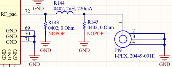
Figure: BL5340 RF pad variant (453-00053) Host PCB 50-Ohm RF trace schematic with series 2nH inductor, RF connector
Layer1 (RF Track and RF GND)
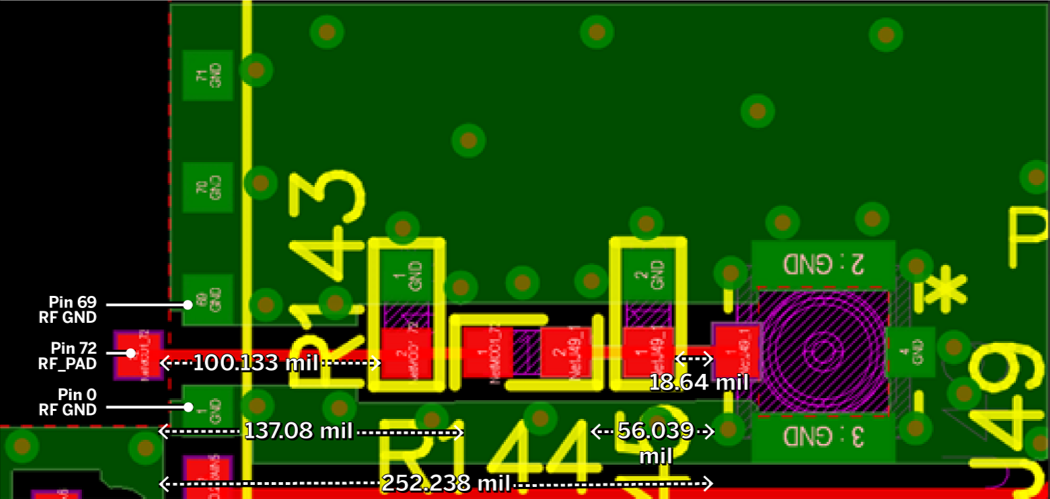
Layer2 (RF GND) and Layer2 copper cut-out under RF connector
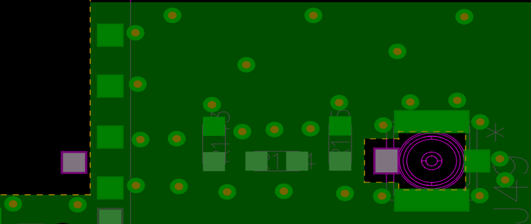
Figure: 50-Ohm RF trace design (Layer1 and Layer2) on BL5340 development board (or host PCB) for use with BL5340 (453-00053) module
Checklist for PCB:
▪ MUST use a 50-Ohm RF trace (GCPW, that is Grounded Coplanar Waveguide) from RF_pad (pin72) of the module (BL5340 453-00053) to RF antenna connector (IPEX MHF4) on host PCB.
▪ To ensure regulatory compliance, MUST follow exactly the following considerations for 50-Ohms RF trace design and test verification:
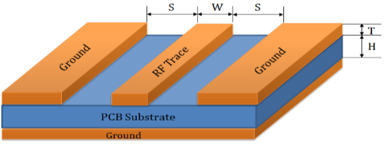
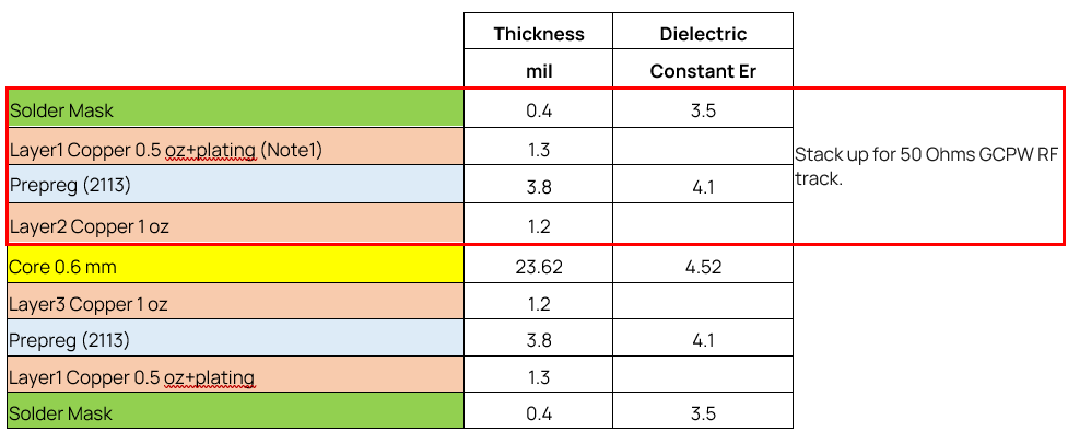
Figure: BL5340 development board PCB stack-up and L1 to L2 50-Ohms Grounded CPW RF trace design
Note 1: The plating (ENIG) above base 0.5 oz copper is not listed, but plating expected to be ENIG.
The 50-Ohms RF trace design MUST be Grounded Coplanar Waveguide (GCPW) with
- Layer1 RF track width (W) of 6.0 mil and
- Layer1 gap (G) to GND of 10 mil and where the
- Layer1 to Layer 2 dielectric thickness (H) MUST be 3.8 mil (dielectric constant Er 4.1).
- Further the Layer1 base copper must be 0.5-ounce base copper (that is 0.7 mil) plus the plating and
- Layer1 MUST be covered by solder mask of 0.4 mil thickness (dielectric constant Er 3.5).
- The 50-Ohms RF trace design MUST follow the PCB stack-up shown in BL5340 development board PCB stack-up and L1 to L2 50-Ohms Grounded CPW RF trace design. (Layer1 to Layer2 thickness MUST be identical to the BL5340 development board).
- The 50-Ohms RF track should be a controlled-impedance trace e.g., ±10%.
- The 50-Ohms RF trace length MUST be identical (as seen in 50-Ohm RF trace design (Layer1 and Layer2) on BL5340 development board (or host PCB) for use with BL5340 (453-00053) module) (252.238mil) to that on the BL5340 development board from BL5340 module RF pad (pin72) to the RF connector IPEX MHF4 Receptable (MPN: 20449-001E).
- Place GND vias regularly spaced either side of 50-Ohms RF trace to form GCPW (Grounded coplanar waveguide) transmission line as shown in 50-Ohm RF trace design (Layer1 and Layer2) on BL5340 development board (or host PCB) for use with BL5340 (453-00053) module and use BL5340 module GND pin1 and GND pin69.
- Cut away copper on Layer2 GND layer under the RF connector IPEX MHF4 Receptable, as seen in 50-Ohm RF trace design (Layer1 and Layer2) on BL5340 development board (or host PCB) for use with BL5340 (453-00053) module. This is to reduce RF detuning the 50Ohms of the RF connector (J49) when it sits on the PCB.
- Cut away copper on Layer2 GND layer under the BL5340 module RF pad (pin72), identical to the BL5340 development board as seen in 50-Ohm RF trace design (Layer1 and Layer2) on BL5340 development board (or host PCB) for use with BL5340 (453-00053) module.
- Use spectrum analyzer to confirm the radiated (and conducted) signal is within the certification limit.
Host PCB Land Pattern and Antenna Keep-out for the 453-00052
SCH symbols (Altium format) and PCB footprints (DXF and Altium format can be found on the BL5340 product page – http://ezurio.com/bl5340-series
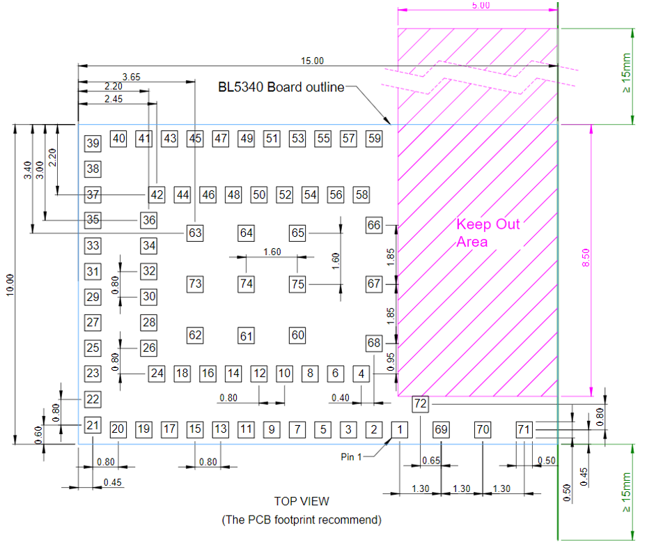
All dimensions are in mm.
Figure: Land pattern and Keep-out for the 453-00052
| Host PCB Land Pattern and Antenna Keep-out for the 453-00052 Notes: | |
| Note 1 | Ensure there is no copper in the antenna ‘keep out area’ on any layers of the host PCB. Also keep all mounting hardware or any metal clear of the area (Refer to Antenna Keep-out and Proximity to Metal or Plastic) to reduce effects of proximity detuning the antenna and to help antenna radiate properly. |
| Note 2 | For the best on-board antenna performance, the module 453-00052 MUST be placed on the edge of the host PCB and preferably in the edge centre and host PCB, the antenna “Keep Out Area” is extended (see Note 4). |
| Note 3 | BL5340 development board has the 453-00052 placed on the edge of the PCB board (and not in corner) for that the Antenna keep out area is extended down to the corner of the development board, see section Host PCB Land Pattern and Antenna Keep-out for the 453-00052. |
| Note 4 | Ensure that there is no exposed copper under the module on the host PCB. |
| Note 5 | You may modify the PCB land pattern dimensions based on their experience and/or process capability. |
External Antenna Integration
External Antenna Integration with the 453-00052
Please refer to the regulatory sections for FCC, ISED, CE, MIC, UKCA and RCM details of use of BL5340 with external antennas in each regulatory region.
The BL5340 family has been designed to operate with the below external antennas (with a maximum gain of
2.0 dBi). The required antenna impedance is 50 ohms. See External antennas for the BL5340. External antennas improve radiation efficiency.
Table: External antennas for the BL5340
| Manufacturer | Model | Ezurio Part Number | Type | Connector | Peak Gain | |
|---|---|---|---|---|---|---|
| 2400-2500 MHz | 2400-2480 MHz | |||||
| Ezurio (Laird Connectivity) | NanoBlue | EBL2400A1-10MH4L | PCB Dipole | IPEX MHF4 | 2 dBi | - |
| Ezurio (Laird Connectivity) | FlexPIFA | 001-0022 | PIFA | IPEX MHF4 | - | 2 dBi |
| Mag.Layers | EDA-8709-2G4C1-B27-CY | 0600-00057 | Dipole | IPEX MHF4 | 2 dBi | - |
| Ezurio (Laird Connectivity) | mFlexPIFA | EFA2400A3S-10MH4L | PIFA | IPEX MHF4 | - | 2 dBi |
| Ezurio (Laird Connectivity) | Laird Connectivity NFC | 0600-00061 | NFC | N/A | - | - |
Application Note for Surface Mount Modules
Introduction
Ezurio surface mount modules are designed to conform to all major manufacturing guidelines. This application note is intended to provide additional guidance beyond the information that is presented in the User Manual. This Application Note is considered a living document and will be updated as new information is presented.
The modules are designed to meet the needs of several commercial and industrial applications. They are easy to manufacture and conform to current automated manufacturing processes.
Reflow Parameters
The Moisture Sensitivity Level (MSL) for this module is MSL 4.
Prior to any reflow, it is important to ensure the modules were packaged to prevent moisture absorption. New packages contain desiccate (to absorb moisture) and a humidity indicator card to display the level maintained during storage and shipment. If directed to bake units on the card, see Recommended baking times and temperatures and follow instructions specified by IPC/JEDEC J-STD-033. A copy of this standard is available from the JEDEC website: http://www.jedec.org/sites/default/files/docs/jstd033b01.pdf
Any modules not manufactured before exceeding their floor life should be re-packaged with fresh desiccate and a new humidity indicator card. Floor life for MSL (Moisture Sensitivity Level) four devices is 72 hours in ambient environment 30°C/60%RH.
Ezurio surface mount modules are designed to be easily manufactured, including reflow soldering to a PCB. Ultimately it is the responsibility of the customer to choose the appropriate solder paste and to ensure oven temperatures during reflow meet the requirements of the solder paste. Ezurio surface mount modules conform to J-STD-020D1 standards for reflow temperatures.
Important: During reflow, modules should not be above 260° and not for more than 30 seconds. In addition, we recommend that the BL5340 module does not go through the reflow process more than one time; otherwise, the BL5340 internal component soldering may be impacted.
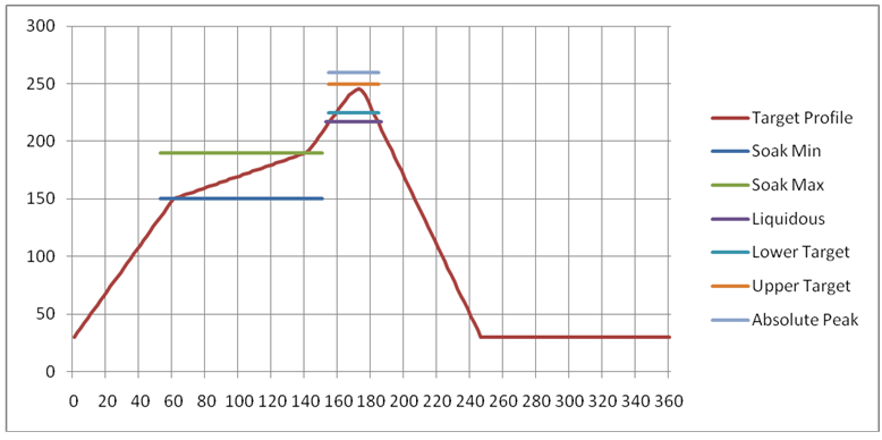
Figure: Recommended reflow temperature
Temperatures should not exceed the minimums or maximums presented in Recommended maximum and minimum temperatures.
Table: Recommended maximum and minimum temperatures
| Specification | Value | Unit |
|---|---|---|
| Temperature Inc./Dec. Rate (max) | 1~3 | °C / Sec |
| Temperature Decrease rate (goal) | 2-4 | °C / Sec |
| Soak Temp Increase rate (goal) | .5 - 1 | °C / Sec |
| Flux Soak Period (Min) | 70 | Sec |
| Flux Soak Period (Max) | 120 | Sec |
| Flux Soak Temp (Min) | 150 | °C |
| Flux Soak Temp (max) | 190 | °C |
| Time Above Liquidous (max) | 70 | Sec |
| Time Above Liquidous (min) | 50 | Sec |
| Time In Target Reflow Range (goal) | 30 | Sec |
| Time At Absolute Peak (max) | 5 | Sec |
| Liquidous Temperature (SAC305) | 218 | °C |
| Lower Target Reflow Temperature | 240 | °C |
| Upper Target Reflow Temperature | 250 | °C |
| Absolute Peak Temperature | 260 | °C |
Soldering Profile / Baking Conditions
Table: Recommended baking times and temperatures
| MSL | 125°C Baking Temp. | 90°C/≤ 5%RH Baking Temp. | 40°C/ ≤ 5%RH Baking Temp. | |||
|---|---|---|---|---|---|---|
| Saturated @ 30°C/85% | Floor Life Limit + 72 hours @ 30°C/60% | Saturated @ 30°C/85% | Floor Life Limit + 72 hours @ 30°C/60% | Saturated @ 30°C/85% | Floor Life Limit + 72 hours @ 30°C/60% | |
| 4 | 11 hours | 7 hours | 37 hours | 23 hours | 15 days | 9 days |
Shipping and Labeling
Packaging
Tape and Reel Package Information
Notes:
- All dimensions are in millimeters.
- Material is High Impact Polystyrene (HIPS)
- Surface resistivity 107~1011Ω/ð
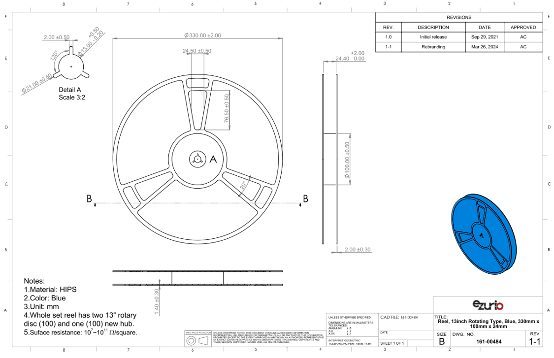
Figure: Reel specifications
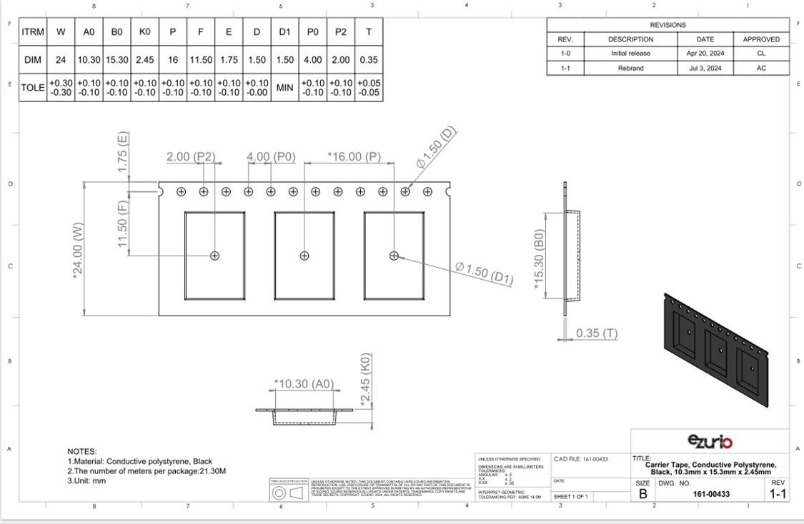
Figure: Tape specifications (Module Orientation – Antenna side of Module away from Tape Holes)
There are 1,000 x BL5340 modules taped in a reel (and packaged in a pizza box) and five boxes per carton (5000 modules per carton). Reel, boxes, and carton are labeled with the appropriate labels. See Carton Contents for more information.
Carton Contents and Packaging Process
The following are the contents of the carton shipped for the BL5340 modules . The example used here is 453-00052R.
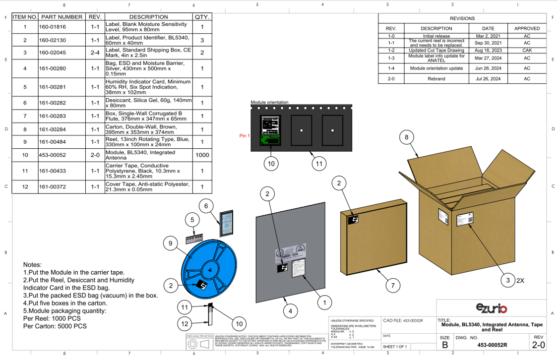
Figure: BL5340 carton contents
Module Orientation in Cavity
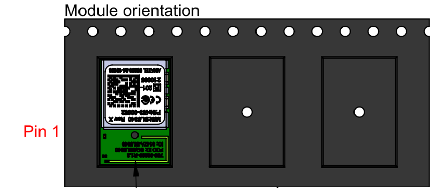
Figure: Module Orientation
Labeling
The following labels are located on the antistatic bag:
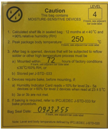
Figure: Antistatic bag labels
The following package label is located on the box:
Figure: Box package label
The following package label is located on both sides of the master carton:
Figure: Master carton package label
Environmental and Reliability
Reliability Tests
The BL5340 module went through the below reliability tests and passed.
| Test Sequence | Test Item | Test Limits and Pass | Test Conditions |
|---|---|---|---|
| 1 | Vibration Test | JESD22-B103B Vibration, Variable frequency | Sample Unpowered Sample Number 3 Vibration Waveform Sine waveform Vibration Frequency/Displacement 20 to 80 Hz/20 g Vibration Frequency/Acceleration 80 to 2000 Hz/20 g Cycle Time 4 minutes Number of Cycles 4 cycles per axis Vibration Axis X, Y, and Z (rotating each axis on vertical vibration table) |
| 2 | Mechanical Shock | JESD22-B104C | Sample Unpowered Sample Number 3 Pulse Shape Half-sine waveform Impact Acceleration 1500 g Pulse Duration 0.5 ms Number of Shocks 30 shocks (5 shocks for each face) Orientation Bottom, top, left, right, front, and rear faces |
| 3 | Thermal Shock | JESD22-A104E Temperature cycling | Sample Unpowered Sample Number 3 Temperature Transition Time Less than 30 seconds Temperature Cycle -40°C (10 minutes), +105°C (10 minutes) Number of Cycles 350 |
Before and after the testing, visual inspection showed no physical defect on samples.
After Vibration test and Mechanical Shock testing, the samples were functionally tested, and all samples functioned as normal. Then after Thermal shock test, the samples were functionally tested, and all samples functioned as normal.
Regulatory, Qualification & Certifications
Regulatory Approvals
For complete regulatory information, refer to the BL5340 Regulatory Information document available from the BL5340 product page.
| Country/Region | Regulatory ID |
|---|---|
| USA (FCC) | SQGBL5340 |
| Canada (ISED) | 3147A-BL5340 |
| UK (UKCA) | N/A |
| EU | N/A |
| Japan (MIC) | 201-210095 |
| Australia (AS) | N/A |
| New Zealand (NZS) | N/A |
| Brazil | 03263-24-10188 |
Bluetooth SIG Qualification
Overview
The Bluetooth Qualification Process promotes global product interoperability and reinforces the strength of the Bluetooth® brand and ecosystem to the benefit of all Bluetooth SIG members. The Bluetooth Qualification Process helps member companies ensure their products that incorporate Bluetooth technology comply with the Bluetooth Patent & Copyright License Agreement and the Bluetooth Trademark License Agreement (collectively, the Bluetooth License Agreement) and Bluetooth Specifications.
The Bluetooth Qualification Process is defined by the Qualification Program Reference Document (QPRD) v3.
To demonstrate that a product complies with the Bluetooth Specification(s), each member must for each of its products:
- Identify the product, the design included in the product, the Bluetooth Specifications that the design implements, and the features of each implemented specification
- Complete the Bluetooth Qualification Process by submitting the required documentation for the product under a user account belonging to your company
The Bluetooth Qualification Process consists of the phases shown below:

To complete the Qualification Process the company developing a Bluetooth End Product shall be a member of the Bluetooth SIG. To start the application please use the following link: Apply for Adopter Membership
Scope
This guide is intended to provide guidance on the Bluetooth Qualification Process for End Products that reference multiple existing designs, that have not been modified, (refer to Section 3.2.2.1 of the Qualification Program Reference Document v3).
For a Product that includes a new Design created by combining two or more unmodified designs that have DNs or QDIDs into one of the permitted combinations in Table 3.1 of the QPRDv3, a Member must also provide the following information:
- DNs or QDIDs for Designs included in the new Design
- The desired Core Configuration of the new Design (if applicable, see Table 3.1 below)
- The active TCRL Package version used for checking the applicable Core Configuration (including transport compatibility) and evaluating test requirements
Any included Design must not implement any Layers using withdrawn specification(s).
When creating a new Design using Option 2a, the Inter-Layer Dependency (ILD) between Layers included in the Design will be checked based on the latest TCRL Package version used among the included Designs.
For the purposes of this document, it is assumed that the member is combining unmodified Core-Controller Configuration and Core-Host Configuration designs, to complete a Core-Complete Configuration.
Qualification Steps When Referencing multiple existing designs, (unmodified) – Option 2a in the QPRDv3
For this qualification option, follow these steps:
- To start a listing, go to: https://qualification.bluetooth.com/
- Select Start the Bluetooth Qualification Process.
- Product Details to be entered:
- Project Name (this can be the product name or the Bluetooth Design name).
- Product Description
- Model Number
- Product Publication Date (the product publication date may not be later than 90 days after submission)
- Product Website (optional)
- Internal Visibility (this will define if the product will be visible to other users prior to publication)
- If you have multiple End Products to list then you can select ‘Import Multiple Products’, firstly downloading and completing the template, then by ‘Upload Product List’. This will populate Qualification Workspace with all your products.
- Specify the Design:
- Do you include any existing Design(s) in your Product? Answer Yes, I do.
- Enter the multiple DNs or QDIDs used in your, (for Option 2a two or more DNs or QDIDs must be referenced)
- Select ‘I’m finished entering DN’s
- Once the DNs or QDIDs are selected they will appear on the left-hand side, indicating the layers covered by the design (should show Core-Controller and Core Host Layers covered).
- What do you want to do next? Answer, ‘Combine unmodified Designs’.
- The Qualification Workspace Tool will indicate that a new Design will be created and what type of Core-Complete configuration is selected.
- An active TCRL will be selected for the design.
- Perform the Consistency Check, which should result in no inconsistencies
- If there are any inconsistencies these will need to be resolved before proceeding
- Save and go to Test Plan and Documentation
Test Plan and Documentation
- As no modifications have been made to the combined designs the tool should report the following message:
‘No test plan has been generated for your new Design. Test declarations and test reports do not need to be submitted. You can continue to the next step.’ - Save and go to Product Qualification fee
- As no modifications have been made to the combined designs the tool should report the following message:
- Product Qualification Fee:
- It’s important to make sure a Prepaid Product Qualification fee is available as it is required at this stage to complete the Qualification Process.
- Prepaid Product Qualification Fee’s will appear in the available list so select one for the listing.
- If one is not available select ‘Pay Product Qualification Fee’, payment can be done immediately via credit card, or you can pay via Invoice. Payment via credit will release the number immediately, if paying via invoice the number will not be released until the invoice is paid.
- Once you have selected the Prepaid Qualification Fee, select ‘Save and go to Submission’
- Submission:
- Some automatic checks occur to ensure all submission requirements are complete.
- To complete the listing any errors must be corrected
- Once you have confirmed all design information is correct, tick all of the three check boxes and add your name to the signature page.
- Now select ‘Complete the Submission’.
- You will be asked a final time to confirm you want to proceed with the submission, select ‘Complete the Submission’.
- Qualification Workspace will confirm the submission has been submitted. The Bluetooth SIG will email confirmation once the submission has been accepted, (normally this takes 1 working day).
Download Product and Design Details (SDoC):
- You can now download a copy of the confirmed listing from the design listing page and save a copy in your Compliance Folder
For further information, please refer to the following webpage:
https://www.bluetooth.com/develop-with-bluetooth/qualification-listing/
Example Design Combinations
The following gives an example of a design possible under option 2a:
Ezurio Controller Subsystem + Nordic nRF Connect SDK Host Subsystem (Ezurio BL5340 based design)
| Design Name | Owner | Design Number (DN) | Link to listing on the SIG website |
| Ezurio BL5340/BL5340PA (Core Controller) | Ezurio | Q361551 | https://qualification.bluetooth.com/ListingDetails/295206 |
| nRF Connect SDK Host component (Core Host) | Nordic Semiconductor ASA | Q358851 | https://qualification.bluetooth.com/ListingDetails/291114 |
Qualify More Products
If you develop further products based on the same design in the future, it is possible to add them free of charge. The new product must not modify the existing design i.e add ICS functionality, otherwise a new design listing will be required.
To add more products to your design, select ‘Manage Submitted Products’ in the Getting Started page, Actions, Qualify More Products. The tool will take you through the updating process.
Ordering Information
| Part Number | Product Description |
|---|---|
| 453-00052R | BL5340 series - Multi-Core / Protocol - Bluetooth® + 802.15.4 + NFC Module (Nordic nRF5340) – Integrated antenna (Tape/Reel) |
| 453-00053R | BL5340 series - Multi-Core / Protocol - Bluetooth® + 802.15.4 + NFC Module (Nordic nRF5340) – Trace Pin (Tape/Reel) |
| 453-00052C | BL5340 series - Multi-Core / Protocol - Bluetooth® + 802.15.4 + NFC Module (Nordic nRF5340) – Integrated antenna (Cut Tape) |
| 453-00053C | BL5340 series - Multi-Core / Protocol - Bluetooth® + 802.15.4 + NFC Module (Nordic nRF5340) – Trace pin (Cut Tape) |
| 453-00052-K1 | Development kit for BL5340 Multi-Core / Protocol - Bluetooth® + 802.15.4 + NFC Module (Nordic nRF5340) – Integrated antenna |
| 453-00053-K1 | Development kit for BL5340 Multi-Core / Protocol - Bluetooth® + 802.15.4 + NFC Module (Nordic nRF5340) - Trace pin (Ext antenna) |
Additional Support & Appendices
Additional Information
Please contact your local sales representative or our support team for further assistance:
| Headquarters | Ezurio 388 S. Main St. Suite 330 Akron, OH 44311 USA |
| Website | http://www.ezurio.com |
| Technical Support | http://www.ezurio.com/resources/support |
| Sales Contact | http://www.ezurio.com/contact |
Note: Information contained in this document is subject to change.
Ezurio’s products are subject to standard Terms & Conditions.
| http://www.ezurio.com | © Copyright 2026 Ezurio All Rights Reserved. Any information furnished by Ezurio and its agents is believed to be accurate but cannot be guaranteed. All specifications are subject to change without notice. Responsibility for the use and application of Ezurio materials or products rests with the end user since Ezurio and its agents cannot be aware of all potential uses. Ezurio makes no warranties as to non-infringement nor as to the fitness, merchantability, or sustainability of any Ezurio materials or products for any specific or general uses. Ezurio or any of its affiliates or agents shall not be liable for incidental or consequential damages of any kind. All Ezurio products are sold pursuant to the Ezurio Terms and Conditions of Sale in effect from time to time, a copy of which will be furnished upon request. Nothing herein provides a license under any Ezurio or any third-party intellectual property right. Ezurio and its associated logos are trademarks owned by Ezurio and/or its affiliates. |
Legacy - Revision History
| Version | Date | Notes | Contributor(s) | Approver |
|---|---|---|---|---|
| 1.0 | 19 Aug 2021 | Final updates for production release | Raj Khatri | Jonathan Kaye |
| 1.1 | 14 Oct 2021 | Update Table 45 (removed unnecessary row) | Raj Khatri | Jonathan Kaye |
| 1.2 | 23 Dec 2021 | Updated Mechanical Details | Dave Drogowski | Andrew Chen |
| 1.3 | 10 Jan 2022 | Updated Other Internal Clocks | Raj Khatri | Dave Drogowski |
| 1.4 | 16 Aug 2023 | Updated Tape and Reel Package Information section | Robert Gosewehr | Dave Drogowski |
| 1.5 | 22 Apr 2024 | Fixed typo | Dave Drogowski | Joe Vattimo |
| 1.6 | 1 Nov 2024 | Updated Bluetooth SIG Qualification | Dave Drogowski | Jonathan Kaye |
| 2.0 | 23 Jan 2025 | Ezurio rebranding | Sue White | Dave Drogowski |
| 2.1 | 4 June 2025 | Updated Bluetooth SIG Qualification | Dave Drogowski | Jonathan Kaye |
| 2.2 | 17 June 2026 | Fixed Japan regulatory ID | Dave Drogowski | Erik Lins |