/filters:background_color(white)/2024-06/BL54L10-Group.png)
/filters:background_color(white)/2024-01/BL54L15-Group.png)
Introduction
Overview
This document describes key hardware aspects of the BL54L15 and BL54L10. This document is intended to assist device manufacturers and related parties with the integration of this radio into their host devices. Data in this document is drawn from several sources. For full documentation on the BL54L15 and BL54L10, visit:
https://www.ezurio.com/bl54l15
https://www.ezurio.com/bl54l10-series
General Description
Experience a new pinnacle of performance, efficiency, and security with our new BL54L15 and BL54L10 series, built on Nordic Semiconductor's powerful nRF54L QFN silicon. Elevating what you know and love from the nRF52 series, this next generation redefines Bluetooth LE and 802.15.4 solutions. Unleashing enhanced processing power, expanded memory, and innovative peripherals, the BL54L15 is the ultimate choice for low power connectivity.
Powered by Nordic's nRF54L15 and nRF54L10 SoC, our compact BL54L15 and BL54L10 modules deliver secure and robust Bluetooth LE and 802.15.4 with flexible programming via Nordic’s nRF Connect SDK or Ezurio Canvas Software Suite.
Featuring a 128MHz ARM Cortex M33 and 128MHz RISC-V coprocessor, supported by 1.5 MB non-volatile memory and 256 KB RAM for BL54L15, 1.0 MB non-volatile memory and 192 KB RAM for BL54L10, the BL54L15 and BL54L10 modules offer double the processing power (vs prior BL654 – nRF52840). The BL54L15 / L10 series brings out all nRF54L15/ L10 hardware features and capabilities including up to +7 dBm transmit power, 1.7V – 3.6V supply considerations, and NFC A-Tag implementation.
It’s further enhanced with state-of-the-art security and is designed for PSA Certified level 3 and supports services such as Secure Boot, Secure Firmware Update, Secure Storage plus protection from physical attacks.
Note: BL54L15/ BL54L10 hardware provides all functionality of the nRF54L15/ nRF54L10 chipset used in the module design. This is a hardware datasheet only – it does not cover the software aspects of the BL54L15 and BL54L10. This is to acknowledge that information in this datasheet is referenced from the nRF54L15/ nRF54L10 datasheet.
This datasheet is subject to change. Please contact Ezurio for further information.
Application Areas
- Building Automation
- Security
- Medical Peripherals
- Industrial Sensors
Features & Benefits
The BL54L15 device features and benefits are described below.
- Nordic nRF54L15/ nRF54L10 – 6x6 mm QFN48 with 31 GPIOs utilized.
- Multi-protocol support: Bluetooth LE, 802.15.4 (Thread & Matter)
- Cortex M33 processor core: 128 MHz ARM Cortex M33
- RISC-V co-processor core: 128 MHz VPR
Memory:
- 1.5MB non-volatile memory, 256 KB RAM for BL54L15
- 1.0MB non-volatile memory, 192 KB RAM for BL54L10
- High Speed Peripherals: - HS-SPI/UART, software defined peripherals on 128 MHz VPR, GPIO - 1x 64 MHz Port, 1.7 – 3.6V, 11 GPIOs
- Low Leakage Peripherals: 2x QDEC, 7x Timer, Global RTC, 2x WDT, NFC A-Tag, TEMP, I2S, COMP, 3x PWM, LPCOMP, 14-bit 8CH ADC, 5x TWI/SPI/UART, GPIO (2x 16 MHz Port (P0, P1), 20 GPIO’s, 1.7-3.6V, 31 GPIO)
- Antenna choice – integrated pre-certified PCB Trace antenna or external antenna support via MHF4 connector
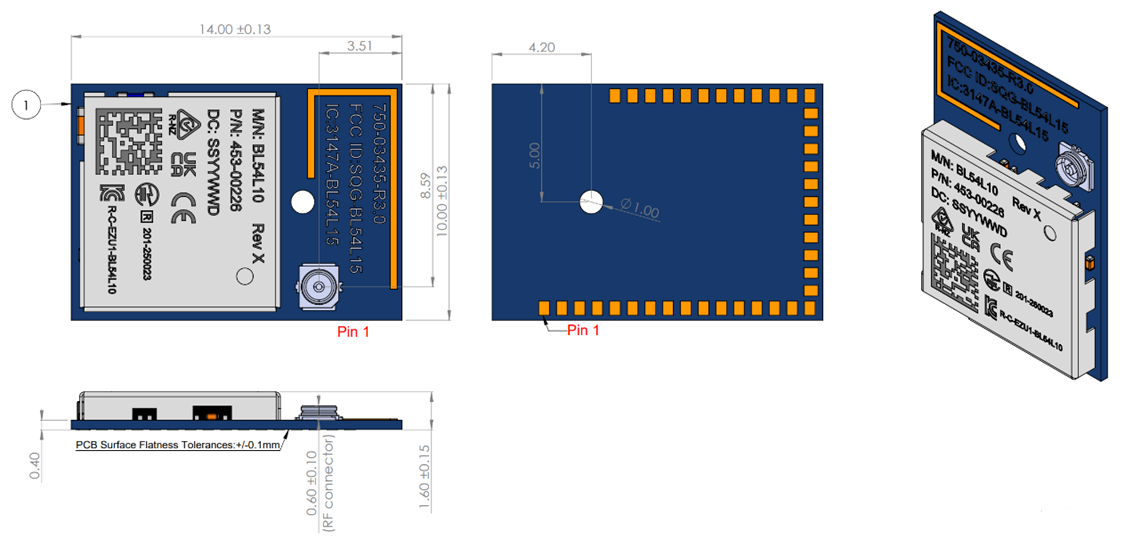
- Ultra-small footprint (14 mm x 10 mm x 1.6 mm)
- Extended Industrial Temperature Rating (-40° to +105 °C)
Specification Summary
Processor / SoC / Chipset
| MPU | Application Core (High Performance):
|
| VPU | Software-Defined Peripheral Core (Ultra-Low Power):
|
| Wireless | Nordic nRF54L15 SoC |
Bluetooth
| Standards | Bluetooth Core 6.2 |
| Bluetooth Radio | Bluetooth Low Energy
|
| Bluetooth LE Features |
|
| PHY | 2405–2480 MHz IEEE 802.15.4-2006 radio transceiver, implementing IEEE 802.15.4-2006 compliant
|
| Proprietary Radio Modes | 2402–2480 MHz Nordic proprietary 1Mbps and 2Mbps modes radio transceiver
|
| Max Transmit Power | +7 dBm - Conducted 453-00001, 453-00225 (Integrated antenna) (Exclude antenna gain) +7 dBm - Conducted 453-00044, 453-00226 (External antenna) (Test at MHF4 connector) |
| Min Transmit Power | -40 dBm |
| Receive Sensitivity(1) (≤37byte packet for BLE) |
|
| Supported Data Rates |
|
| Link Budget | 101 dB @ BLE 1 Mbps (TX power used is 7dBm) 109 dB @ BLE 125 kbps (TX power used is 7dBm) |
NFC
| NFC-Type A Listen mode compliant | Based on NFC forum specification: 13.56 MHz, Date rate 106 kbps, NFC Type2 and Type 4 emulation Modes of Operation: Disable, Sense, Activated Use Cases: Touch-to-Pair with NFC, NFC enabled Out-of-Band Pairing |
| Security | Designed for PSA Certified Level 3 with Secure Boot, Secure Firmware Update, and Secure Storage. Integrated tamper sensors detect attacks and take action, and cryptographic accelerators are hardened against side-channel attacks. |
Radio Performance
| Antenna Options | Internal:
External:
|
Interfaces
| Memory Interfaces |
|
| Peripheral Interface | 31x Multifunction I/O lines |
|---|---|
| HS-UART | Application Core (High Performance):
|
| GPIO | Up to 31 multifunction GPIO’s:
Application Core (High Performance):
Software defined peripheral Core (Ultra-Low Power):
|
| ADC (14-bit) | Application Core (High Performance):
|
| Global RTC (GRTC) | Software defined peripheral Core (Ultra-Low Power):
|
| RTC | Software defined peripheral Core (Ultra-Low Power):
|
| PWM | Software defined peripheral Core (Ultra-Low Power):
|
| I2C | 2x |
| SPI/UART/TWI | Software defined peripheral Core (Ultra-Low Power):
|
| TEMP | Software defined peripheral Core (Ultra-Low Power):
|
| I2S | Software defined peripheral Core (Ultra-Low Power):
|
| PDM | Software defined peripheral Core (Ultra-Low Power):
|
| TIMER | Software defined peripheral Core (Ultra-Low Power):
|
| QDEC | Software defined peripheral Core (Ultra-Low Power):
|
| COMP | Software defined peripheral Core (Ultra-Low Power):
|
| LPCOMP | Software defined peripheral Core (Ultra-Low Power): 1x LPCOMP (low power comparator) |
| WDT | Software defined peripheral Core (Ultra-Low Power):
|
| NFC A-Tag | Software defined peripheral Core (Ultra-Low Power):
|
| Wakeup Pins | Software defined peripheral Core (Ultra-Low Power):
|
| Ext. 32.768 KHz Crystal | Software defined peripheral Core (Ultra-Low Power):
|
Power
| Supply Voltage | Normal Voltage Mode (VDD_nRF): 1.7V-3.6V (Internal DCDC convertor or LDO) |
Mechanical
| Dimensions | 14mm x 10mm x 1.6mm Pad Pitch – 0.75 mm Pad Type – Three rows of pads (LGA - Land Grid Array). |
| Weight | <1 gram |
Software
| Security | Designed for PSA Certified Level 3 with Secure Boot, Secure Firmware Update, and Secure Storage. Integrated tamper sensors detect attacks and take action, and cryptographic accelerators are hardened against side-channel attacks.
|
| Programmability Options | Via SWD (JTAG) 2 wire interface:
|
| Firmware Update | Via SWD (JTAG) 2 wire interface or UART |
Environmental
| Operating Temperature | -40 ˚C to +105 ˚C |
| Storage Temperature | -40 ˚C to +105 ˚C |
| Lead Free | Lead-free and RoHS Compliant |
Certifications
| Regulatory Compliance | FCC/ISED/CE/MIC/RCM/UKCA/KC |
| Bluetooth SIG | Full Bluetooth SIG Declaration ID |
Development
| Development Kit | Development kit per module SKU (453-00001-K1 and 453-00044-K1 respectively, BL54L15 only) Utilise the above development kits for projects planned with BL54L10. |
| Development Tools |
|
| Debug | ITM parallel trace |
Warranty
| Warranty Terms | One Year Warranty |
Functional Descriptions
Programming & Firmware
The BL54L15/BL54L10 module is shipped from Ezurio manufacturing facilities with no firmware programmed.
BL54L15 BL54L10 Firmware Options
Firmware for use with the BL54L15/BL54L10 can be divided into the following types.
- Bootloader – This is the application that resides on the Application Core used to perform firmware updates of the Application and FLPR cores.
The MCU Boot or Trusted Firmware M Bootloaders are recommended to be used as the basis for the BL54L15 Bootloader functionality.
- Application – This is the main application running on the Application core. In interfaces with the integrated radio stack(s) and provides supplementary functionality in addition to the time critical activities performed for radio activity.
- Software Defined Peripheral – This is the application running on the RISC-V FLPR core.
Clocks
HFXO - 32MHz crystal oscillator and nRF54L15/nRF54L10 internal load capacitor mandatory setting
The BL54L15/BL54L10 module contains the 32 MHz crystal, but the load capacitors to create 32MHz crystal oscillator circuit are inside the nRF54L15/nRF54L10 chipset. Customer can set the internal nRF54L15/nRF54L10 capacitors from 4 pF to 17 pF in 0.25pF if needed or use default value without changing.
The 32 MHz crystal inside the BL54L15/BL54L10 module is a high accuracy crystal (±15 ppm at room temperature) that helps with radio operation and reducing power consumption in the active modes.
LFCLK – Low Frequency clock source
There are four possibilities (see figure 3) for the low frequency clock (LFCLK) and options are:
LFRC (32.768kHz RC oscillator): The Internal 32.768 kHz RC oscillator (LFRC) is fully embedded in nRF54L15/nRF54L10 (and does not require additional external components) with an accuracy ±250 ppm (after calibration of LFRC at least every eight seconds using the HFXO as a reference oscillator).
LFXO (32.768kHz crystal oscillator): For higher LFCLK accuracy (greater than ±250ppm accuracy is required), the low frequency crystal oscillator (LFXO) must be used. To use LFXO, a 32.768kHz crystal must be connected between the XL1 and XL2 pins and the load capacitance between each crustal terminal and ground. Optionally internal (to nRF54L15/nRF54L10) capacitor of maximum 18 pF in 0.5 pF steps are provided on pins XL1 and XL2.
Low frequency (32.768 kHz) external source: The 32.768 kHz oscillator (LFXO) is designed to work with external sources
LFSYNTH (32.768kHz Synthesised clock) from HFCLK (LFSYNTH): The LFCLK can be synthesised from the HFCLK source. LFSYNTH depends on the HFCLK to run. The accuracy of the LFCLK clock with LFSYNTH as a source assumes the accuracy of the HFCLK. If high accuracy is required, the HFCLK must generated from the HFXO. Using the LFSYNT clock removes the requirement for an external 32.768kHz crystal but the increases the average power consumption as the HFCLK will turned on in the system.
Other Internal Clocks
Hardware Architecture
Block Diagrams
Pin-Out
| Pin # | Pin Name (bold coloured pins for clock for interfaces, trace) | nRF54L15 nRF54L10 QFN48 Pin | nRF54L15/ nRF54L10 QFN48 Name | Description | Example usage |
|---|---|---|---|---|---|
| 1 | GND | - | VSS | ||
| 2 | P2.09 | 20 | P2.09/TRACEDATA[2]/SPI.SDI/SDO | General purpose I/O Trace data SPIM SDI SPIS SDI UARTE CTS | Trace SPIM00/SPIM21 SPIS00/SPIS21 UARTE00/UARTE21 |
| 3 | P2.08 | 19 | P2.08/TRACEDATA[1]/SPI.SDI/SDO | General purpose I/O Trace data SPIM SDO SPIS SDO UARTE TXD | Trace SPIM00/SPIM21 SPIS00/SPIS21 UARTE00/UARTE21 |
| 4 | P2.07 | 18 | P2.07/TRACEDATA[0]/SWO/SPI.DCX | General purpose I/O Trace data Serial wire output (SWO) SPIM DCX UARTE RXD | Trace Trace SPIM00/SPIM21 UARTE00/UARTE21 |
| 5 | SWDIO | 25 | SWDIO | Serial Wire Debug IO for debug and programming | |
| 6 | SWDCLK | 26 | SWDCLK | Serial Wire Debug clock input for debug and programming | |
| 7 | NRESET | 30 | nRESET | Pin RESET with internal pull-up resistor (13k Ohms). System Reset (Active Low). | |
| 8 | P2.02 | 13 | P2.02/SPI.SDI/SDO | General purpose I/O SPIM SDO SPIS SDO UARTE TXD QSPI D0 Serial wire output (SWO) | SPIM00/SPIM20 SPIS00/SPIS20 UARTE00/UARTE20 FLPR Trace |
| 9 | P2.00 | 11 | P2.00/SPI.DCX | General purpose I/O SPIM DCX UARTE RXD QSPI D3 | SPIM00/SPIM20 UARTE00/UARTE20 FLPR (QSPI) |
| 10 | P2.01/CLK | 12 | P2.01/SPI.SCK | General purpose I/O SPIM SCK SPIS SCK QSPI SCK | Clock pin SPIM00/SPIM20 SPIS00/SPIS20 FLPR |
| 11 | P2.04 | 15 | P2.04/SPI.SDI/SDO | General purpose I/O SPIM SDI SPIS SDI UARTE CTS QSPI D1 | SPIM00/SPIM20 SPIS00/SPIS20 UARTE00/UARTE20 FLPR |
| 12 | P2.05 | 16 | P2.05/SPI.CS | General purpose I/O SPIM CS UARTE RTS QSPI CS | SPIM00/SPIM20 UARTE00/UARTE20 FLPR |
| 13 | P2.03 | 14 | P2.03 | General purpose I/O QSPI D2 | FLPR |
| 14 | P1.03/NFC2/CLK | 4 | P1.03/NFC2 | General purpose I/O Dedicated pin for NFC input | Clock pin |
| 15 | P1.02/NFC1 | 3 | P1.02/NFC1 | General purpose I/O Dedicated pin for NFC input | |
| 16 | GND | ||||
| 17 | P0.00 | 23 | P0.00 | General purpose I/O | |
| 18 | P0.01 | 24 | P0.01 | General purpose I/O | |
| 19 | P0.02 | 27 | P0.02 | General purpose I/O | |
| 20 | P1.07/AIN3 | 8 | P1.07/AIN3/TAMPC | General purpose I/O TAMPC active shield 1 input Analog input | TAMPC |
| 21 | P1.06/AIN2 | 7 | P1.06/AIN2/TAMPC | General purpose I/O TAMPC active shield 1 output Analog input | TAMPC |
| 22 | P1.05/AIN1 | 6 | P1.05/AIN1/TAMPC | General purpose I/O TAMPC active shield 0 input RADIO DFEGPIO Analog input | TAMPC RADIO |
| 23 | P1.04/AIN0/CLK | 5 | P1.04/AIN0/TAMPC | General purpose I/O TAMPC active shield 0 output Analog input | Clock pin TAMPC |
| 24 | P1.01/XL2 | 2 | P1.01/XL2 | General purpose I/O General purpose I/O Connection for 32.768kHz crystal | Ezurio Devkit: Optional 32.768kHz crystal pad XL2, XL1 and associated 9pF load capacitor inside nRF54L15 chipset. |
| 25 | P1.00/XL1 | 1 | P1.00/XL1 | General purpose I/O Connection for 32.768kHz crystal | Ezurio Devkit: Optional 32.768kHz crystal pad XL2, XL1 and associated 9pF load capacitor inside nRF54L15 chipset. |
| 26 | VDD_nRF | 48 | VDD | 1.7V-3.6V input for Normal Voltage Mode where connect external supply to VDD_nRF(pin26). | |
| 27 | GND | ||||
| 28 | P1.10 | 38 | P1.10/TAMPC | General purpose I/O TAMPC active shield 2 input RADIO DFEGPIO | TAMPC RADIO |
| 29 | P1.09 | 37 | P1.09/TAMPC | General purpose I/O TAMPC active shield 2 output RADIO DFEGPIOO | TAMPC RADIO |
| 30 | P1.08/EXTREF/CLK16M/CLK | 9 | P1.08/CLK16M/TAMPC | General purpose I/O GRTC HF clock output External reference for SAADC | Clock pin |
| 31 | P0.04/CLK | 29 | P0.04/GRTC_CLKOUT32K | General purpose I/O GRTC LF clock output | Clock pin GRTC |
| 32 | P1.14/AIN7 | 42 | P1.14/AIN7 | General purpose I/O RADIO DFEGPIO Analog input | RADIO |
| 33 | P1.13/AIN6 | 41 | P1.13/AIN6 | General purpose I/O RADIO DFEGPIO Analog input | RADIO |
| 34 | P1.12/AIN5/CLK | 40 | P1.12/AIN5 | General purpose I/O TAMPC active shield 3 input RADIO DFEGPIO Analog input | Clock pin TAMPC RADIO |
| 35 | P1.11/AIN4/CLK | 39 | P1.11/AIN4 | General purpose I/O TAMPC active shield 3 output RADIO DFEGPIO Analog input | Clock pin TAMPC RADIO |
| 36 | P0.03/CLK | 28 | P0.03/GRTC_PWMOUT | General purpose I/O GRTC PWM output | Clock pin GRTC |
| 37 | P2.10 | 21 | P2.10/TRACEDATA[3]/SPIM.CS | General purpose I/O Trace SPIM CS UARTE RTS | Trace SPIM00/SPIM21 UARTE00/UARTE21 |
| 38 | P2.06/CLK | 17 | P2.06/TRACECLK/SPI.SCK | General purpose I/O SPIM SCK SPIS SCK Trace clock | Clock pin SPIM00/SPIM21 SPIS00/SPIS21 Trace |
| 39 | GND |
Notes:
Note 1 (GPIO):
- GPIO = General Input or Output (GPIO level voltage tracks VDD pin). AIN =Analog input.
- If GPIO is selected as an input, ensure the input is not floating (which can cause current consumption to drive with time in low power modes (such as System ON Idle), by selecting the internal pull up or pull down.
- Must connect all GND pads to host board PCB GND plane.
Note2 (Clock for serial interfaces or trace):
- Some peripherals (SPI, TWI, PDM, I2S, TRACE, GRTC) have clock signals. Dedicated clock pins have been optimized to ensure correct timing relationship between clock and data signal for these peripherals. Pins that can be used as clock signals are shown with pin name in red colour.
- The peripheral data signal must be configured to use pins close to the clock pin. This ensures that the
- internal paths from the peripheral to the pin have the same delay, so that the data and clock signals reach
- the pins at the same time.
- For high-speed signals, the printed circuit board (PCB) layout must use short PCB traces of identical length. This makes sure any delays are kept to a minimum and it assures close to identical delay and clock path.
Note 3 (Dedicated pins):
- UARTE20/21: Can use any pin son GPIO port P1. Can be connected across power domains to dedicated pin on P2.
- SPIM00: Has dedicated pins on GPIO port P2. For 32MHz operation, the pins must be configured using extra high drive E0/E1 configuration.
- SPIM20/21: Can use any pin son GPIO port P1. Can be connected across power domains to dedicated pin on P2.
- SPIS20/21: Can use any pin son GPIO port P1. Can be connected across power domains to dedicated pin on P2.
- TRACE: Has dedicated pins on GPIO port P2. For 32MHz operation, the pins must be configured using extra high drive E0/E1 configuration.
- GRTC: Has dedicated pins for clock and PWM output.
- TAMPC: Has dedicated pins for active shield inputs and outputs.
- FLPR: Uses dedicated pins on GPIO port P2 for emulated peripherals such as QSPI.
- RADIO: Uses dedicated pins on GPIO port P1 for antenna switch control (DFEGPIO for direction finding).
- NFC: Uses dedicated pins listed in pin definitions table.
Note 4 (SWDIO / SWCLK / nRESET / VDD / GND):
- Customer MUST bring out SWDIO, SWCLK, nRESET, VDD, GND for programming purposes.
Power Supply
Mechanical Drawings
3D models for BL54L15 Module, MHF4 (453-00044) and BL54L15 Module, Trace Antenna (453-00001) on the BL54L15 product page – https://www.ezurio.com/product/bl54l15-series-bluetooth-le-80215-4-nfc
Electrical Characteristics
Absolute Maximum Ratings
Absolute maximum ratings are the extreme limits for supply voltage and voltages on digital and analogue pins of the module are listed below; exceeding these values causes permanent damage.
| Parameter | Min | Max | Unit |
|---|---|---|---|
| Supply Voltages | |||
| VDD_nRF | -0.3 | 3.9 | V |
| VDD_nRFext | -0.3 | 3.7 | V |
| I/O pin voltage | |||
| Voltage at GPIO pin (at VDD≤3.6V) | -0.3 | VDD_nRF + 0.3 | V |
| Voltage at GPIO pin (at VDD>3.6V) | 3.9 | V | |
| Voltage at GPIO pin under extended operating temperature (at VDD≤3.4V) | -0.3 | VDD_nRF + 0.3 | V |
| Voltage at GPIO pin under extended operating temperature (at VDD>3.4V) | -0.3 | 3.7 | V |
| NFC antenna pin current (NFC1/2) | - | 130 | mA |
| Environmental | |||
| Storage temperature | -40 | +125 | ºC |
| MSL (Moisture Sensitivity Level) | - | 4 | - |
| ESD (as per EN301-489) Conductive Air Coupling | 4 8 | kV kV | |
| Flash Memory (Endurance) (Note 2) | 10,000 | Write/erase cycles | |
| Flash Memory (Retention) | 10 years at 85ºC 2 years at 105ºC | years at TBD ºC |
Note 1: The absolute maximum rating for VDD pin (max) is 3.9 V for the BL54L15.
Note 2: Wear levelling can be implemented by customer.
Recommended Operating Conditions
Power supply operating parameters
| Parameter | Min | Typ | Max | Unit |
|---|---|---|---|---|
| VDD_nRF (independent of DCDC) supply range | 1.7 | 3.6 | V | |
| VDD_nRFext (VDD_nRF supply voltage under extended operating temperature) | 1.7 | 3.4 | V | |
| VDD_nRF Maximum ripple or noise (See Note 1) | - | - | 10 | mV |
| Operating Temperature Range | -40 | +25 | +85 | ºC |
| Extended operating temperature | 85 | 105 | ºC |
Note 1: This is the maximum VDD_nRF ripple or noise (at any frequency) that does not disturb the radio.
Note 2: The on-board power-on reset circuitry may not function properly for rise times longer than the specified maximum.
Note 3: Some electrical parameters are valid only for the operating temperature range conditions. When this is the case, an additional parameter for the extended operating temperature condition is provided.
Power Management & Consumption
Power Consumption
| Active Modes Peak Current (for max Tx power +7dBm)– Radio only | 30 mA peak Tx, 15mA avg TX@ 1.8V, LE1M 25 mA peak Tx, 23mA avg TX@ 1.8V, CW 17 mA peak Tx, 8.3mA avg TX@ 3.3V, LE1M 14 mA peak Tx, 12.6mA avg TX@ 3.3V, CW | ||||
| Active Modes Peak Current (for Tx power -40dBm) – Radio only | 8 mA peak Tx, 2.5mA avg TX @ 1.8V, LE1M 7 mA peak Tx, 3.1mA avg TX@ 1.8V, CW 6.5 mA peak Tx, 2.1mA avg TX @ 3.3V, LE1M 5 mA peak Tx, 2.6mA avg TX @ 3.3V, CW | ||||
| Active Modes Average Current | Depends on many factors. | ||||
| Ultra-low Power Modes |
|
Integration Guidelines
Host PCB Land Pattern and Antenna Keep-Out
PCB footprint - BL54L15 (DXF and Altium format) and SCH Symbol - BL54L15 (Altium format) can be found on the BL54L15 product page – https://www.ezurio.com/product/bl54l15-series-bluetooth-le-80215-4-nfc
BL54L10 use the same footprint of BL54L15.
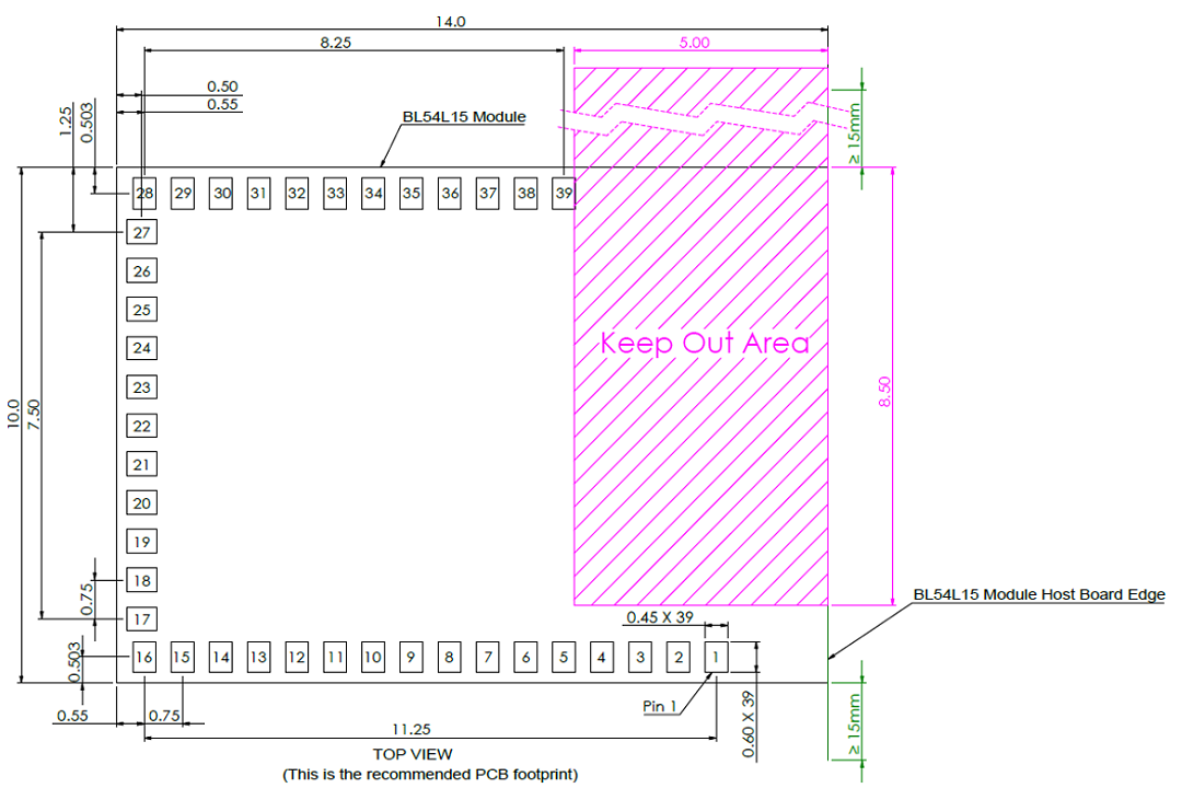
All dimensions are in mm.
Notes:
- Ensure there is no copper in the antenna ‘keep out area’ on any layers of the host PCB. Also keep all mounting hardware or any metal clear of the area (Refer to 7.3.2) to reduce effects of proximity detuning the antenna and to help antenna radiate properly.
- For the best on-board antenna performance, the module 453-00001/453-00225 MUST be placed on the edge of the host PCB and preferably in the edge center and host PCB, the antenna “Keep Out Area” is extended (see Note 4).
- BL54L15 development board has the 453-00001 placed on the edge of the PCB board (and not in corner) for that the Antenna keep out area is extended down to the corner of the development board, see section 8.2 Host PCB Land Pattern and Antenna Keep-out for the 453-00001 and 453-00225.
- Ensure that there is no exposed copper under the module on the host PCB.
- You may modify the PCB land pattern dimensions based on their experience and/or process capability.
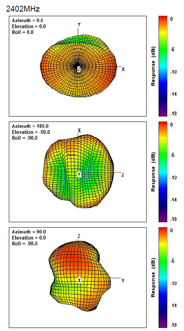
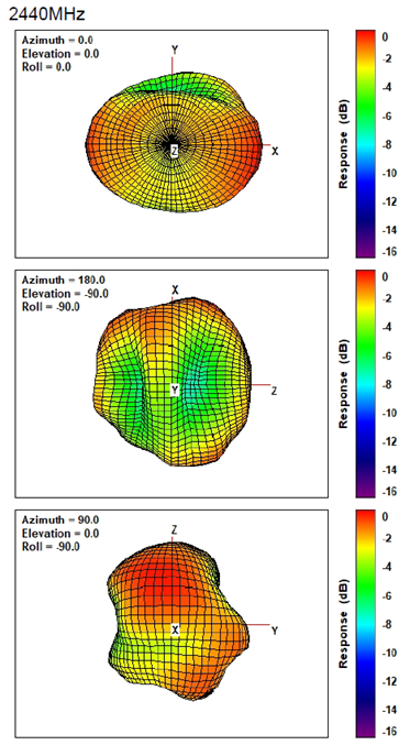
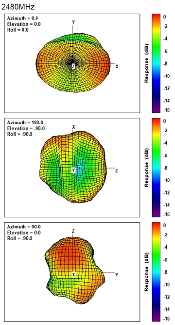
On-Board PCB Trace Antenna Characteristics
Summary of Antenna Performance
| 2402 MHz Peak | 2402 MHz Avg | 2440 MHz Peak | 2440 MHz Avg | 2480 MHz Peak | 2480 MHz Avg | |
|---|---|---|---|---|---|---|
| 453-00001/453-00225 PCB trace antenna | +0.2dBi | -4.24dBi | +1.49dBi | -3.19dBi | +1.39dBi | -3.27dBi |
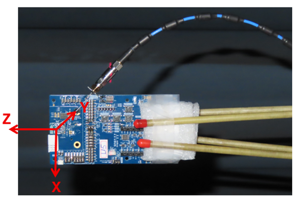
Radiated Performance
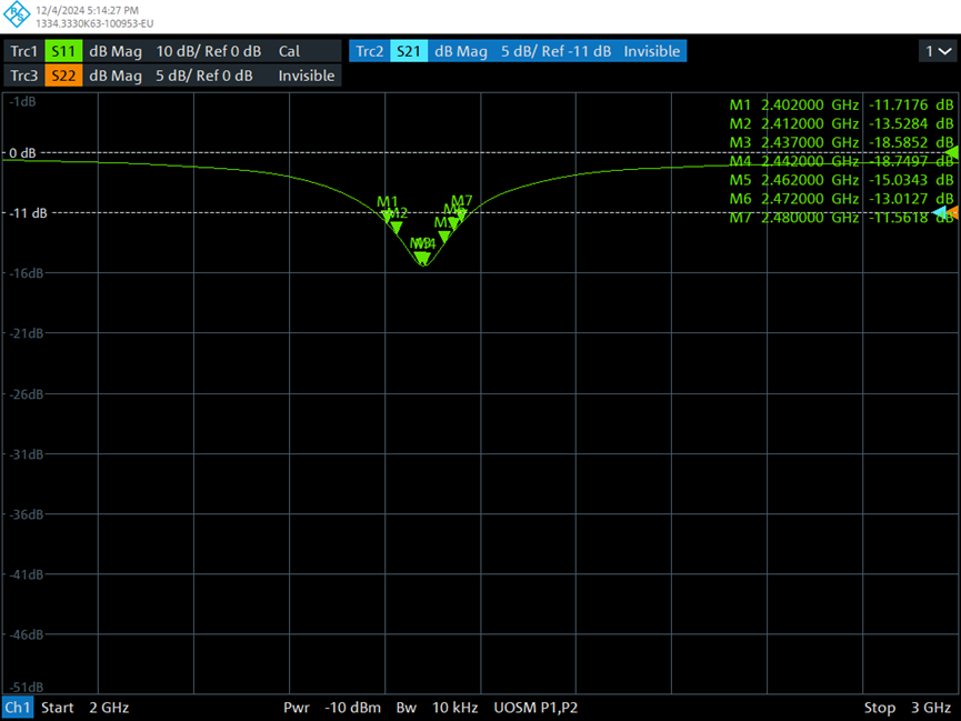
Antenna S11 Measuring Data
Software Requirements Related to Hardware
32MHz crystal internal load capacitor setting
BL54L15/ BL54L10 module contains the 32 MHz crystal but the load capacitors to create 32 MHz crystal oscillator circuit are inside the nRF54L15/ nRF54L10 chipset. Customer can set the internal nRF54L15/nRF54L10 capacitors from 4 pF to 17 pF in 0.25pF if needed, or use default value without changing.
Circuit (Overview and Checklist)
The BL54L15/ BL54L10 is easy to integrate, requiring one mandatory external 10uF capacitor on customers board and apart from that those components which customer require for development and in your end application.
The following are suggestions for your design for the best performance and functionality.
Checklist (for Schematic):
- BL54L15/ BL54L10 power supply:
Normal voltage mode power supply mode is entered when the external supply voltage (1.7V-3.6V) is connected to both VDD_nRF pin (pin26).
External power source should be within the operating range, rise time and noise/ripple specification of the BL54L15/ BL54L10. Add decoupling capacitors for filtering the external source. Power-on reset circuitry within BL54L15/ BL54L10 series module incorporates brown-out detector, thus simplifying your power supply design. Upon application of power, the internal power-on reset ensures that the module starts correctly.
- AIN (ADC) and GPIO pin IO voltage levels:
BL54L15/BL54L10 GPIO voltage levels are at VDD_nRF. Ensure input voltage levels into GPIO pins are at VDD_nRF also. Ensure ADC pin maximum input voltage for damage is not violated.
- AIN (ADC) impedance and external voltage divider setup:
If you need to measure with ADC a voltage higher than 3.6V, you can connect a high impedance voltage divider to lower the voltage to the ADC input pin.
- SWD:
This is REQUIRED for loading firmware. MUST wire out the SWD two wire interface on host design. Five lines should be wired out, namely SWDIO, SWDCLK, nRESET, GND and VDD.
- UART and flow control (CTS, RTS):
Required if customer requires UART.
- TWI (I2C):
It is essential to remember that pull-up resistors on both SCL and SDA lines are required, the value as per I2C standard. nRF54L15/ nRF54L10 can provide 13K Ohms typical pull up values internally. For other values, fit external pull-up resistor on both SCL and SDA as per I2C specification to set speed. The I2C specification allows a line capacitance of 400pF.
- QSPI, High Speed SPI, High speed TWI (I2C, 1Mbps) and Trace:
High-Speed SPI, TWI and Trace come on dedicated GPIO pins only. Other lower speed SPI and TWI can come out on any GPIO pins.
For all high-speed signal, the printed circuit board (PCB) layout must ensure that connections are made using short PCB traces.
- GPIO pins
If GPIO is selected as an input, ensure the input is not floating (which can cause current consumption to drive with time in low power modes (such as System ON Idle), by selecting the internal pull up or pull down.
- NFC antenna connector: To make use of the Ezurio flexi-PCB NFC antenna (part # 0600-00061), fit connector:
Description – FFC/FPC Connector, Right Angle, SMD/90d, Dual Contact,1.2 mm Mated Height
Manufacturer – Molex
Manufacturers Part number – 512810594
Add tuning capacitors of 300 pF on NFC1 pin to GND and 300 pF on NFC2 pins to GND if the PCB track length is similar as development board.
- nRESET pin (active low):
Hardware reset. Wire out to push button or drive by host.
By default module is out of reset when power applied to VDD_nRF pins (13K pull-up inside BL54L15/ BL54L10 (nRF54L15-QFAA/nRF54L10-QFAA)).
- Optional External 32.768kHz crystal:
If the optional external 32.768kHz crystal is needed, then use a crystal that meets specification and add load capacitors (either inside nRF54L15-QFAA/nRF54L10-QFAA or discrete capacitors outside BL54L15/BL54L10 (nRF54L15-QFAA/nRF54L10-QFAA) whose values should be tuned to meet all specification for frequency and oscillation margin.
PCB Layout
PCB Layout on Host PCB - General
Checklist (for PCB):
- MUST locate BL54L15/ BL54L10 module close to the edge of PCB (mandatory for the 453-00001/453-00225 for on-board PCB trace antenna to radiate properly).
- Use solid GND plane on inner layer (for best EMC and RF performance).
- All module GND pins MUST be connected to host PCB GND.
- Place GND vias close to module GND pads as possible.
- Unused PCB area on surface layer can flooded with copper but place GND vias regularly to connect the copper flood to the inner GND plane. If GND flood copper is on the bottom of the module, then connect it with GND vias to the inner GND plane.
- Route traces to avoid noise being picked up on VDD_nRF supply and AIN (analogue), GPIO (digital) traces and high-speed traces.
- Ensure no exposed copper is on the underside of the module (refer to land pattern of BL54L15/BL54L10 development board).
Antenna Keep-Out on Host PCB
The 453-00001/453-00225 has an integrated PCB trace antenna and its performance is sensitive to host PCB. It is critical to locate the 453-00001/453-00225 on the edge of the host PCB (or corner) to allow the antenna to radiate properly. Refer to guidelines in section PCB land pattern and antenna keep-out area for the 453-00001/453-00225. Some of those guidelines repeated below.
- Ensure there is no copper in the antenna keep-out area on any layers of the host PCB. Keep all mounting hardware and metal clear of the area to allow proper antenna radiation.
- For best antenna performance, place the 453-00001/453-00225 module on the edge of the host PCB, preferably in the edge center.
- The BL54L15 development board (453-00001-K1) has the 453-00001 module on the edge of the board (not in the corner). The antenna keep-out area is defined by the BL54L15 development board which was used for module development and antenna performance evaluation is shown in Figure 6, where the antenna keep-out area is ~5mm wide, ~28.6mm long; with PCB dielectric (no copper) height ~1.57mm sitting under the 453-00001 PCB trace antenna module. Bl54L10 module (453-00225) please follow the same design of BL54L15.
- The 453-00001 PCB trace antenna is tuned when the 453-00001 is sitting on development board (host PCB) with size of 113 mm x 63.5 mm x 1.6mm.
- A different host PCB thickness dielectric will have small effect on antenna.
- The antenna-keep-out defined in the 8.2 Host PCB Land Pattern and Antenna Keep-out for the 453-00001 and 453-00225 section.
Host PCB land pattern and antenna keep-out for the BL54L15/BL54L10 applies when the 453-00001/453-00225 is placed in the edge of the host PCB preferably in the edge center. Below shows an example.
Note 1: The BL54L15/BL54L10 module is placed on the edge, preferably edge centre of the host PCB.
Note 2: Copper cut-away on all layers in the Antenna Keep-out area under the 453-00001/453-00225 on host PCB.
Antenna Keep-out and Proximity to Metal or Plastic
Checklist (for metal /plastic enclosure):
- Minimum safe distance for metals without seriously compromising the antenna (tuning) is 40 mm top/bottom and 30 mm left or right.
- Metal close to the 453-00001/453-00225 PCB trace monopole antenna (bottom, top, left, right, any direction) will have degradation on the antenna performance. The amount of that degradation is entirely system dependent, meaning you will need to perform some testing with your host application.
- Any metal closer than 20 mm will begin to significantly degrade performance (S11, gain, radiation efficiency).
- It is best that you test the range with a mock-up (or actual prototype) of the product to assess effects of enclosure height (and materials, whether metal or plastic) and host PCB ground (GND plane size).
External Antenna Integration with BL54L15/BL54L10 MHF4 variant (453-00044/453-00226)
Please refer to the regulatory sections for FCC, ISED, CE, MIC, UKCA and RCM details of use of BL54L15 with external antennas in each regulatory region.
The BL54L15/BL54L10 family has been designed to operate with the below external antennas (with a maximum gain of
2.32 dBi). The required antenna impedance is 50 ohms. See the table below. External antennas improve radiation efficiency.
External antennas for the BL54L15/BL54L10 RF trace pin variant module (453-00044/453-00226)
| Manufacturer | Model | Ezurio Part Number | Type | Connector | Peak Gain 2400-2500 MHz | Peak Gain2400-2480 MHz |
|---|---|---|---|---|---|---|
| Ezurio (Laird Connectivity) | NanoBlue | EBL2400A1-10MH4L | PCB Dipole | IPEX MHF4 | 2 dBi | - |
| Ezurio (Laird Connectivity) | FlexPIFA | 001-0022 | PIFA | IPEX MHF4 | - | 2 dBi |
| Mag.Layers | EDA-8709-2G4C1-B27-CY | 0600-00057 | Dipole | IPEX MHF4 | 2.32 dBi | - |
| Ezurio (Laird Connectivity) | mFlexPIFA | EFA2400A3S-10MH4L | PIFA | IPEX MHF4 | - | 2 dBi |
| Ezurio (Laird Connectivity) | iFlexPIFA Mini | EFG2401A3S-10MH4L | PIFA | IPEX MHF4 | - | 2 dBi |
| Ezurio (Laird Connectivity) | Ezurio NFC | 0600-00061 | NFC | N/A | - | - |
Application Note for Surface Mount Modules
Introduction
Ezurio’s surface mount modules are designed to conform to all major manufacturing guidelines. This application note is intended to provide additional guidance beyond the information that is presented in the user manual. This application note is considered a living document and will be updated as new information is presented.
The modules are designed to meet the needs of several commercial and industrial applications. They are easy to manufacture and conform to current automated manufacturing processes.
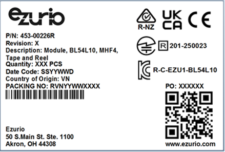
Part numbers – 453-00001R/453-00225R and 453-00044R/453-00226R are shipped as Tape / Reel, with a reel containing 1,000 pcs.
Shipping
All modules are shipped in tape and reel package and sealed in ESD Bags.
Labeling
MSL Label
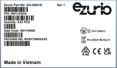
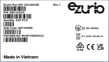
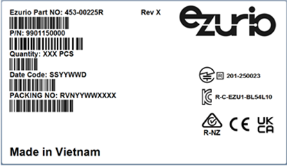
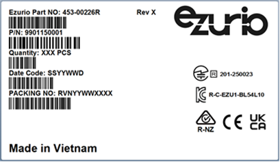
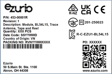
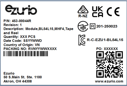
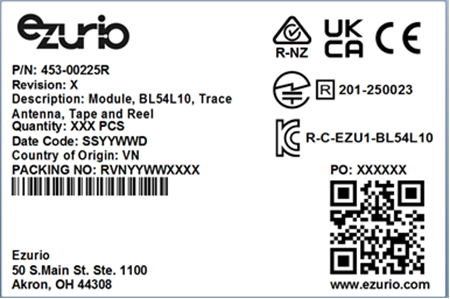
Product Identifier Labels
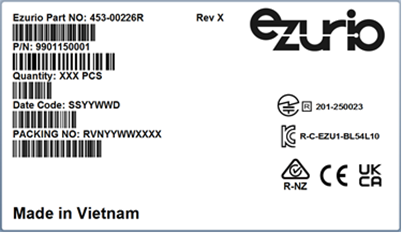
The following labels are placed on the pizza box.
The following labels are placed on the master shipping carton.
Recommended Stencil Aperture
When soldering, the stencil thickness should be ≥ 0.1 mm.
Reflow Parameters/ Soldering
Convection reflow or IR/Convection reflow (one-time soldering or two-time soldering in air or nitrogen environment)
- Measuring point – IC package surface
Temperature profile:
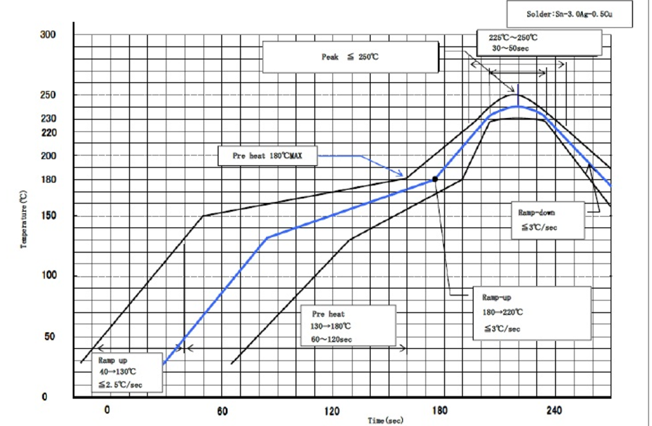
- Ramp-up: 40-130˚C. Less than 2.5˚C/sec
- Pre heat: 130-180˚C 60-120 sec, 180˚C MAX
- Ramp-up: 180-220˚C. Less than 3˚C/sec
Peak Temperature: MAX 250˚C
- 225˚C ~ 250˚C, 30 ~ 50 sec
- Ramp-down: Less than 3˚C/sec
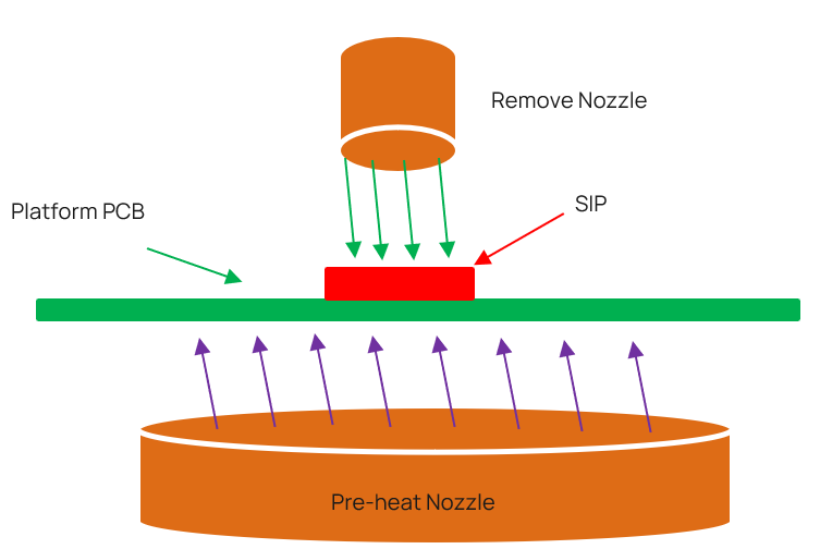
Cautions when Removing the BL54L15/BL54L10 from the Platform for RMA
- Bake the platform PCBA before removing the BL54L15/BL54L10 module from the platform.
- Remove the BL54L15/BL54L10 module by using a hot air gun. This process should be carried out by a skilled technician.
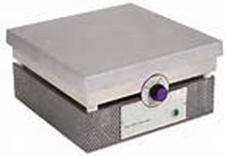
Recommended conditions for one-side component platform:
- Set the hot plate at 280°C.
- Put the platform on the hot plate for 8~10 seconds.
- Remove the device from platform.
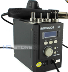
Recommended conditions for two-side components platform:
- Use two hot air guns.
- On the bottom, use a pre-heated nozzle (temp setting of 200~250°C) at a suitable distance from the platform PCB.
On the top, apply a remove nozzle (temp setting of 330°C). Heat until device can be removed from platform PCB.
- Remove the residue solder under the bottom side of device. (Note: Alternate module pictured as an example)
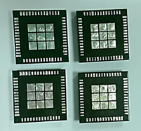 |  |
| (Not accepted for RMA) | (Accepted for RMA analysis) |
- Remove and clean the residue flux as needed.
Precautions for Use
- Opening/handing/removing must be done on an anti-ESD treated workbench. All workers must also have undergone anti-ESD treatment.
- The devices should be mounted within one year of the date of delivery.
- The BL54L15/BL54L10 modules are MSL 4 rated.
Environmental and Reliability
Environmental Requirements
Required Storage Conditions
Prior to Opening the Dry Packing
The following are required storage conditions prior to opening the dry packing:
- Normal temperature: 5~40˚C
- Normal humidity: 80% (Relative humidity) or less
- Storage period: One year or less
Note: Humidity means relative humidity.
After Opening the Dry Packing
The following are required storage conditions after opening the dry packing (to prevent moisture absorption):
Storage conditions for one-time soldering:
- Temperature: 5-25°C
- Humidity: 60% or less
- Period: 72 hours or less after opening
Storage conditions for two-time soldering
Storage conditions following opening and prior to performing the 1st reflow:
- Temperature: 5-25°C
- Humidity: 60% or less
- Period: A hours or less after opening
Storage conditions following completion of the 1st reflow and prior to performing the 2nd reflow
- Temperature: 5-25°C
- Humidity: 60% or less
- Period: B hours or less after completion of the 1st reflow
Note: Should keep A+B within 72 hours.
Temporary Storage Requirements after Opening
The following are temporary storage requirements after opening:
- Only re-store the devices once prior to soldering.
- Use a dry box or place desiccant (with a blue humidity indicator) with the devices and perform dry packing again using vacuumed heat-sealing.
The following indicate the required storage period, temperature, and humidity for this temporary storage:
Storage temperature and humidity:
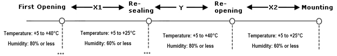
*** - External atmosphere temperature and humidity of the dry packing
Storage period:
- X1+X2 – Refer to Material handling information
- Required Storage Conditions. Keep is X1+X2 within 72 hours.
- Y – Keep within two weeks or less.
Baking Conditions
Baking conditions and processes for the module follow the J-STD-033 standard which includes the following:
- The calculated shelf life in a sealed bag is 12 months at <40℃ and <80% relative humidity.
- Once the packaging is opened, the SiP must be mounted (per MSL4/Moisture Sensitivity Level 4) within 72 hours at <30˚C and <60% relative humidity.
If the SiP is not mounted within 72 hours or if, when the dry pack is opened, the humidity indicator card displays >10% humidity, then the product must be baked for 48 hours at 125 ˚C (±5 ˚C).
Reflow Profile
Reliability Tests
Climatic and Dynamic
Climatic and Dynamic Reliability Test Results for BL54L15/BL54L10 Modules
| Test Item | Specification | Standard | Test Result |
|---|---|---|---|
| Thermal Shock | Temperature: -40 ~ 105℃ Ramp time: Less than 10 seconds. Dwell Time: 10 minutes Number of Cycles: 350 times | *JESD22-A106 *IEC 60068-2-14 for dwell time and number of cycles | PASS |
| Vibration Non-Operating Unpackaged device | Vibration Wave Form: Sine Waveform Vibration frequency / Displacement: 20-80 Hz/1.5mm Vibration frequency / Acceleration: 80-2000 Hz/20g Cycle Time: 4 min/cycle Number of Cycles: 4 cycle/axis Vibration Axes: X, Y and Z (Rotate each axis on vertical vibration table) | JEDEC 22-B103B (2016) | PASS |
| Mechanical Shock Non-Operating Unpackaged device | Pulse shape: Half-sine waveform Impact acceleration: 1500 g Pulse duration: 0.5 ms Number of shocks: 30 shocks (5 shocks for each face) Orientation: Bottom, top, left, right, front, and rear faces | JEDEC 22-B110B.01 (2019) | PASS |
Reliability Prediction
MTBF Predictions for BL54L15/BL54L10 Modules
| Ezurio Part Number | Environment | Standard | Test Result 45 ℃ (Hours) |
| 453-00001R 453-00001C 453-00225R 453-00225C | Ground, Fixed, Uncontrolled | Telcordia Issue 4 | 1,559,211 |
| 453-00044R 453-00044C 453-00226R 453-00226C | Ground, Fixed, Uncontrolled | Telcordia Issue 4 | 1,559,211 |
| 453-00001R 453-00001C 453-00225R 453-00225C | Mobile, Fixed, Uncontrolled | Telcordia Issue 4 | 605,957 |
| 453-00044R 453-00044C 453-00226R 453-00226C | Mobile, Fixed, Uncontrolled | Telcordia Issue 4 | 605,957 |
| Ezurio Part Number | Environment | Standard | Test Result 105 ℃ (Hours) |
| 453-00001R 453-00001C 453-00225R 453-00225C | Ground, Fixed, Uncontrolled | Telcordia Issue 4 | 980,517 |
| 453-00044R 453-00044C 453-00226R 453-00226C | Ground, Fixed, Uncontrolled | Telcordia Issue 4 | 980,517 |
| 453-00001R 453-00001C 453-00225R 453-00225C | Mobile, Fixed, Uncontrolled | Telcordia Issue 4 | 283,138 |
| 453-00044R 453-00044C 453-00226R 453-00226C | Mobile, Fixed, Uncontrolled | Telcordia Issue 4 | 283,138 |
Regulatory, Qualification & Certifications
Regulatory Approvals
Full regulatory information on the BL54L15/BL54L10, including the Regulatory Information Guide, grants, and test reports are available on the BL54L15 product page and BL54L10 product page.
The BL54L15/BL54L10 holds current certifications in the following countries:
BL54L15 Certifications
| Country/Region | Regulatory ID |
|---|---|
| USA (FCC) | SQG-BL54L15 |
| EU (ETSI) | N/A (No ID Number Required) |
| UKCA | N/A (No ID Number Required) |
| Canada (ISED) | 3147A-BL54L15 |
| Japan (MIC) | 201-250023 |
| Australia (RCM) | N/A |
| New Zealand (RCM) | N/A |
| Korea | R-C-EZU1-BL54L15 (for BL54L15) R-C-EZU1-BL54L10 (for BL54L10) |
Certified Antennas
| Model | MPN | Manufacturer | Type | Connector | Peak Gain (2400 – 2500 MHz) |
|---|---|---|---|---|---|
| NanoBlue | EBL2400A1-10MH4L | Ezurio | PCB Dipole | IPEX MHF4 | 2 dBi |
| FlexPIFA | 001-0022 | Ezurio | FlexPIFA | IPEX MHF4L | 2 dBi |
| EDA-8709-2G4C1-B27-CY | EDA-8709-2G4C1-B27-CY (Ezurio Part#0600-00057) | MAG.LAYERS | Dipole | IPEX MHF4 | 2.32 dBi |
| mFlexPIFA | EFA2400A3S-10MH4L | Ezurio | PIFA | IPEX MHF4L | 2 dBi |
| I-FlexPIFA Mini Series | EFG2401A3S-10MHF4L | Ezurio | I-FlexPIFA | IPEX MHF4L | 2 dBi |
| Ezurio NFC | 0600-00061 | Ezurio | Coiled Inductor | FFC/FPC Connector | - |
Bluetooth SIG Qualification
The Bluetooth Qualification Process promotes global product interoperability and reinforces the strength of the Bluetooth® brand and ecosystem to the benefit of all Bluetooth SIG members. The Bluetooth Qualification Process helps member companies ensure their products that incorporate Bluetooth technology comply with the Bluetooth Patent & Copyright License Agreement and the Bluetooth Trademark License Agreement (collectively, the Bluetooth License Agreement) and Bluetooth Specifications.
The Bluetooth Qualification Process is defined by the Qualification Program Reference Document (QPRD).
To demonstrate that a product complies with the Bluetooth Specification(s), each member must for each of its products:
- Identify the product, the design included in the product, the Bluetooth Specifications that the design implements, and the features of each implemented specification
- Complete the Bluetooth Qualification Process by submitting the required documentation for the product under a user account belonging to your company
The Bluetooth Qualification Process consists of the phases shown below:

To complete the Qualification Process the company developing a Bluetooth End Product shall be a member of the Bluetooth SIG. To start the application please use the following link if you are not already a Bluetooth SIG Member: Apply for Adopter Membership, (Associate Membership also available which has a yearly membership fee).
Scope
This guide is intended to provide guidance on the Bluetooth Qualification Process for End Products that reference a single existing design, that has not been modified, (refer to Section 3.2.1 of the Qualification Program Reference Document (QPRD).
This option applies to a Member qualifying a Product that includes an existing Design that has a DN, QDID, or DID and that Design has not been modified (e.g., rebranding a Qualified Product from another Member). The Design identified by the DN, QDID, or DID may only implement Bluetooth Specifications that are active or deprecated at the time of Submission. No modifications may be made to the Design, including changes to the ICS Form.
Changes to the Product outside the Design are allowed, including:
- Enabling technologies
- Changes to the industrial design
- Changes to the communication technology other than Bluetooth
- Changes to the features that are unrelated to Bluetooth, branding, packaging, colour, shape, Product name, or Model number
Members are responsible for assessing that modifications to the Product outside of the Design do not affect compliance with Bluetooth Specifications or result in a change to the ICS Form.
For the purposes of this document, it is assumed that the member is combining a single unmodified Core-Complete Configuration.
Qualification Steps When Referencing a single existing design, (unmodified) – Option 1 in the QPRD
For this qualification option, follow these steps:
- To start a listing, go to: https://qualification.bluetooth.com/
- Select Start the Bluetooth Qualification Process.
Product Details to be entered:
- Project Name (this can be the product name or the Bluetooth Design name).
- Product Description
- Model Number
- Product Publication Date (the product publication date may not be later than 90 days after submission)
- Product Website (optional)
- Internal Visibility (this will define if the product will be visible to other users prior to publication)
- If you have multiple End Products to list then you can select ‘Import Multiple Products’, firstly downloading and completing the template, then by ‘Upload Product List’. This will populate Qualification Workspace with all your products.
Specify the Design:
- Do you include any existing Design(s) in your Product? Answer Yes, I do.
- Enter the single DN or QDID used in your, (for Option 1 only one DN or QDID can be referenced)
- Once the DN or QDID is selected it will appear on the left-hand side, indicating the layers covered by the design.
- Select ‘I’m finished entering DN’s
- What do you want to do next? Answer, ‘Use this Design without Modification’
- Save and go to Product Qualification Fee
Test Plan and Documentation
- As no modifications have been made to the combined designs the tool should report the following message:
‘No test plan has been generated for your new Design. Test declarations and test reports do not need to be submitted. You can continue to the next step.’ - Save and go to Product Qualification fee
- As no modifications have been made to the combined designs the tool should report the following message:
Product Qualification Fee:
- Do you include any existing Design(s) in your Product? Answer Yes, I do.
- Enter the single DN or QDID used in your, (for Option 1 only one DN or QDID can be referenced)
- Once the DN or QDID is selected it will appear on the left-hand side, indicating the layers covered by the design.
- Select ‘I’m finished entering DN’s
- What do you want to do next? Answer, ‘Use this Design without Modification’
- Save and go to Product Qualification Fee
Submission:
- Some automatic checks occur to ensure all submission requirements are complete.
- To complete the listing any errors must be corrected
- Once you have confirmed all design information is correct, tick all of the three check boxes and add your name to the signature page.
- Now select ‘Complete the Submission’.
- You will be asked a final time to confirm you want to proceed with the submission, select ‘Complete the Submission’.
- Qualification Workspace will confirm the submission has been submitted. The Bluetooth SIG will email confirmation once the submission has been accepted, (normally this takes 1 working day).
Download Product and Design Details (SDoC):
- You can now download a copy of the confirmed listing from the design listing page and save a copy in your Compliance Folder
For further information, please refer to the following webpage:
https://www.bluetooth.com/develop-with-bluetooth/qualification-listing/
Example Design Combinations
The following gives an example of a design possible under option 1:
Ezurio End Product design using Nordic Component based design
| Design Name | Owner | Design ID | Link to listing on the SIG website | Core Spec Version |
|---|---|---|---|---|
| BL54L15/ BL54L15µ | Ezurio | Q345095 | https://qualification.bluetooth.com/ListingDetails/274104 | 6.0 |
| BL54L15/ BL54L15µ | Ezurio | Q387119 | https://qualification.bluetooth.com/ListingDetails/334158 | 6.2 |
Qualify More Products
If you develop further products based on the same design in the future, it is possible to add them free of charge. The new product must not modify the existing design i.e add ICS functionality, otherwise a new design listing will be required.
To add more products to your design, select ‘Manage Submitted Products’ in the Getting Started page, Actions, Qualify More Products. The tool will take you through the updating process.
Ordering Information
| Part Number | Product Description |
|---|---|
| 453-00001R | Module, BL54L15, (Nordic nRF54L15), Trace antenna, Tape/Reel |
| 453-00044R | Module, BL54L15, (Nordic nRF54L15), MHF4 Connector, Tape/Reel |
| 453-00001C | Module, BL54L15, (Nordic nRF54L15), Trace antenna, Cut Tape |
| 453-00044C | Module, BL54L15, (Nordic nRF54L15), MHF4 Connector, Cut Tape |
| 453-00001-K1 | Development kit, Module, BL54L15 (Nordic nRF54L15), Trace antenna |
| 453-00044-K1 | Development kit, Module, BL54L15 (Nordic nRF54L15), MHF4 Connector |
| 453-00225R | Module, BL54L10, (Nordic nRF54L10), Trace antenna, Tape/Reel |
| 453-00226R | Module, BL54L10, (Nordic nRF54L10), MHF4 Connector, Tape/Reel |
| 453-00225C | Module, BL54L10, (Nordic nRF54L10), Trace antenna, Cut Tape |
| 453-00226C | Module, BL54L10, (Nordic nRF54L10), MHF4 Connector, Cut Tape |
Legacy - Revision History
| Version | Date | Notes | Contributor(s) | Approver |
|---|---|---|---|---|
| 0.1 | 10 June 2024 | Initial PRELIMINARY release. | Raj Khatri | Jonathan Kaye |
| 0.2 | 2 Oct 2024 | Updated pin list names and notes below table1. Added section External Antenna Integration with BL54L15/BL54L10 MHF4 variant (453-00044/453-00226) | Raj Khatri | Jonathan Kaye |
| 0.3 | 24 Oct 2024 | Removed Medium voltage mode (VDDM_nRF) from Specification Summary table and updated Normal voltage mode (VDD_nRF) operating range from 1.7V-2.6V to 1.7V-3.6V. Updated Block Diagram and Pin-out for 39 connection pins. Updated SCH symbol to remove pin40. Updated pin list in Table 1 (removed pin 40 VDDM_nRF). Updated BL54L15/ BL54L10 Power Supply Updated Table 4 external antenna Mag Layers EDA-8709-2G4C1-B27-CY antenna gain from 2dBi to 2.32dBi. | Raj Khatri | Jonathan Kaye |
| 0.4 | 6 Dec 2024 | Updated maximum Tx power to +7 dBm. | Dave Drogowski | Jonathan Kaye |
| 0.5 | 11 Dec 2024 | Updated sensitivity value Added trace antenna performance | Louis Chang | Jonathan Kaye |
| 0.6 | 16 Dec 2024 | Updated maximum Tx power to +6 dBm. | Louis Chang | Jonathan Kaye |
| 1.0 | 16 Dec 2024 | Initial release | Dave Drogowski | Jonathan Kaye |
| 1.1 | 19 Dec 2024 | Updated maximum Tx power to +7 dBm. | Louis Chang | Jonathan Kaye |
| 1.2 | 13 Jan 2025 | Updated title of 7.4 Updated some typo | Louis Chang | Jonathan Kaye |
| 1.3 | 21 Feb. 2025 | Change (VDD_nRF) operating range from 1.7V-3.6V to 1.7V-3.5V. Add VDD_nRFsupply voltage (1.7V-3.3V) under extended operating Temperature (85 to 105C) Update Absolute maximum ratings of VDD_nRF (-0.3V-3.6V) | Louis Chang | Jonathan Kaye |
| 1.4 | 25 Feb. 2025 | Update Minimum Transmit Power Setting to -40dBm Update Active Modes Peak Current | Louis Chang | Jonathan Kaye |
| 1.5 | 27 Feb. 2025 | Update 32MHz crystal oscillator internal capacitor setting value Update 32.768KHz crystal oscillator internal capacitor setting value Update NFC antenna pin current value | Louis Chang | Jonathan Kaye |
| 1.6 | 3 Mar. 2025 | Update Idle mode and off mode current BL54L10 Antenna performance shares with BL54L15 | Louis Chang | Jonathan Kaye |
| 1.7 | 10 Mar. 2025 | Update Radiated Performance Update flash specs in Absolute Maximum Ratings | Louis Chang | Jonathan Kaye |
| 1.8 | 18 Mar 2025 | Update power consumption in 2.1 | Louis Chang | Jonathan Kaye |
| 1.9 | 09 Jun 2025 | Update Thermal shock Max. Temperature from 85℃ to 105℃ of Reliability Test | Olivia Chang | Jonathan Kaye |
| 2.0 | 27 Nov 2025 | Update average power consumption in 2.1 | Louis Chang | Jonathan Kaye |
| 2.1 | 3 Dec 2025 | Update Operation conditions and Absolute maximum ratings in 3.3 | Louis Chang | Jonathan Kaye |
| 2.2 | 16 Dec 2025 | Update On -Board PCB Trace Antenna Characteristics | Louis Chang | Jonathan Kaye |