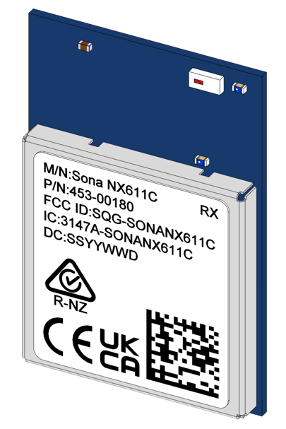
/filters:background_color(white)/2025-12/Sona%20NX611%20-%20Family.png)
Introduction
This document describes key hardware aspects of Ezurio Connectivity’s Sona™NX611 Wi-Fi6 / Bluetooth 5.4 modules, which are based on NXP’s IW611 chipset. It serves as a preliminary supplement to the full module datasheet and is provided to assist in initial hardware integration.
Note: Data in this document is drawn from several sources and is subject to change.
Sona™ NX611 M.2 1218 Module
This section describes the hardware footprint, mechanical drawing and hardware pinout of the Sona NX611 M.2 1218 Chip Antenna module. It provides details and pin assignments critical to hardware integration of the module.
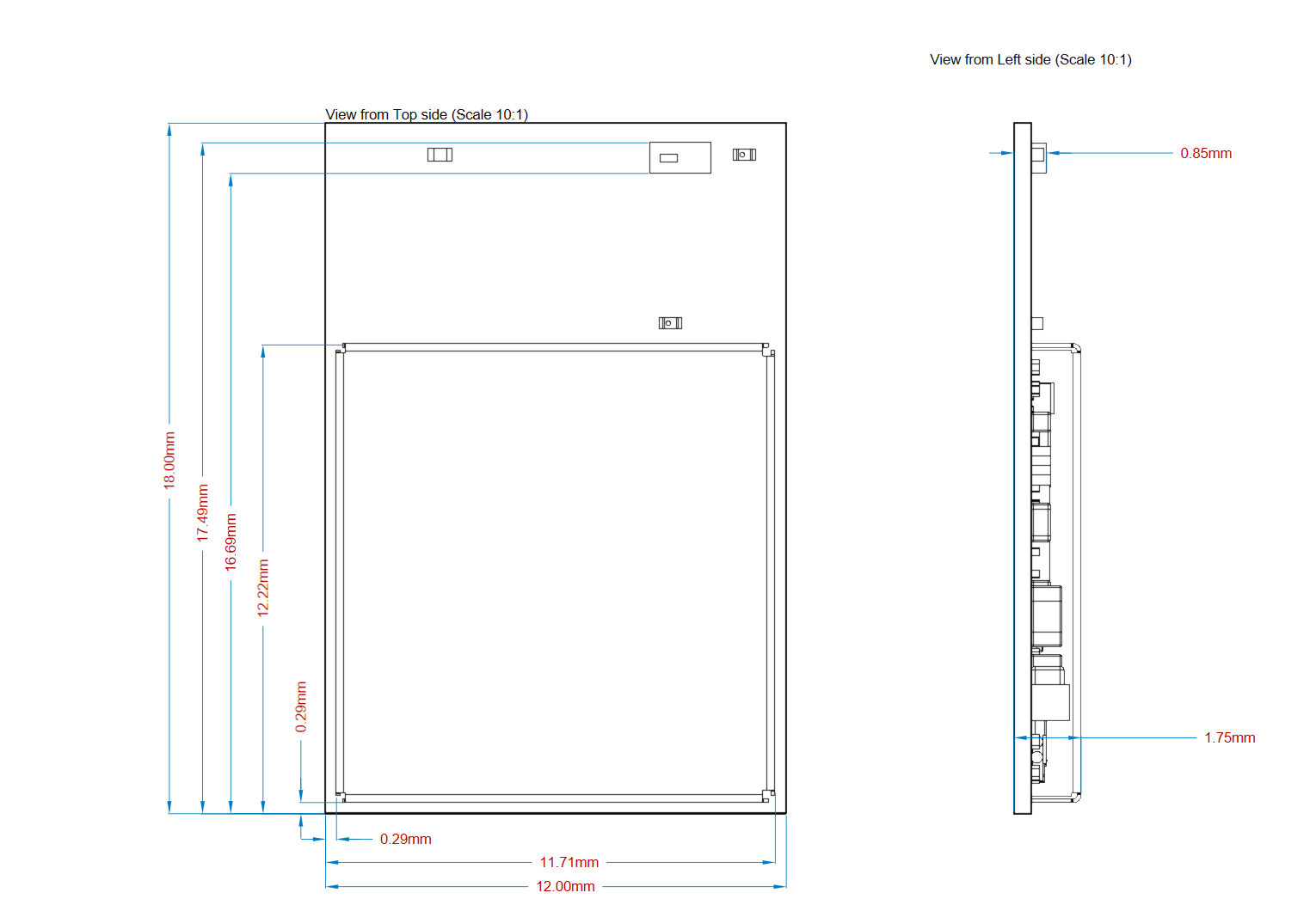
Detail drawings are shown in Figure 2andFigure 3.
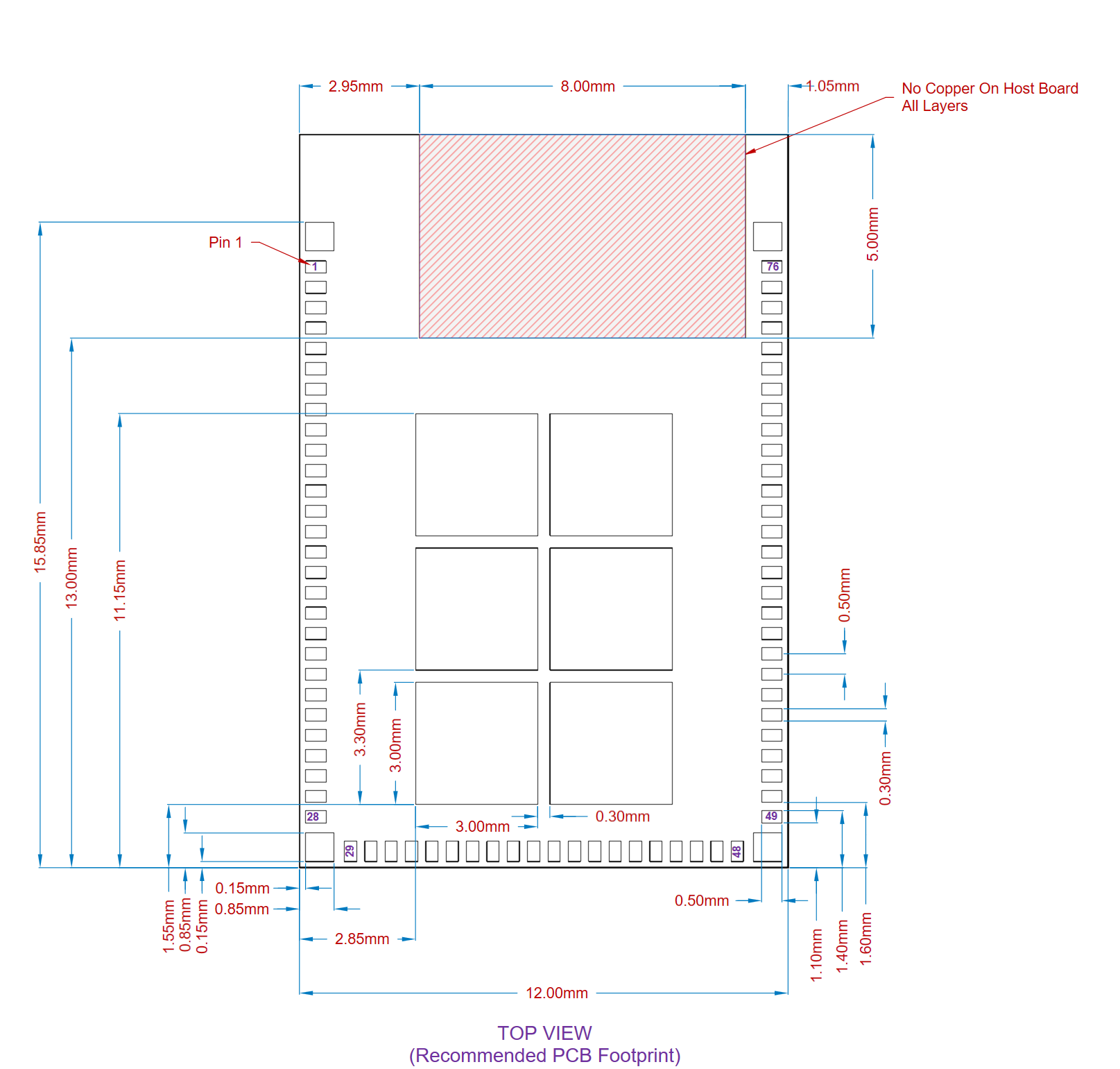
Sona™ NX611 M.2 1218 Module PCB Footprint
Sona™ NX611 M.2 1218 Module Mechanical Drawing
Sona™ NX611 M.2 1218 Module Pinout
Table 1: Sona NX611 M.2 1218 Chip Antenna Module Pinout
| Pin Number | PCIe M.2 Name | Pin Name NX611 | Description |
|---|---|---|---|
| 1 | UIM_POWER_SRC/GPIO1 | UNUSED | |
| 2 | UIM_POWER_SNK | UNUSED | |
| 3 | UIM_SWP | UNUSED | |
| 4 | 3.3V | 3.3V | |
| 5 | 3.3V | 3.3V | |
| 6 | GND | Ground | Ground |
| 7 | RESERVED | UNUSED | |
| 8 | ALERT# | NC | |
| 9 | I2C_CLK | NC | |
| 10 | I2C_DATA | NC | |
| 11 | COEX_RXD | COEX_RXD | |
| 12 | COEX_TXD | COEX_TXD | |
| 13 | COEX3 | UNUSED | |
| 14 | SYSCLK/GNSS_0 | UNUSED | |
| 15 | TX_BLANKING/GNSS_1 | UNUSED | |
| 16 | RESERVED | UNUSED | |
| 17 | GND | Ground | Ground |
| 18 | RESERVED | UNUSED | |
| 19 | RESERVED | NC | |
| 20 | GND | Ground | Ground |
| 21 | PETn1 | UNUSED | |
| 22 | PETp1 | UNUSED | |
| 23 | GND | Ground | |
| 24 | PERn1 | UNUSED | |
| 25 | PERp1 | UNUSED | |
| 26 | GND | Ground | |
| 27 | SUSCLK(32kHz) | UNUSED | |
| 28 | W_DISABLE1# | PDn | |
| 29 | PEWAKE# | UNUSED | |
| 30 | CLKREQ# | UNUSED | |
| 31 | PERST# | UNUSED | |
| 32 | GND | Ground | Ground |
| 33 | REFCLKn0 | UNUSED | |
| 34 | REFCLKp0 | UNUSED | |
| 35 | GND | Ground | Ground |
| 36 | PETn0 | UNUSED | |
| 37 | PETp0 | UNUSED | |
| 38 | GND | Ground | Ground |
| 39 | PERn0 | UNUSED | |
| 40 | PERp0 | UNUSED | |
| 41 | GND | Ground | Ground |
| 42 | VENDOR DEFINED | EXT_PRI | |
| 43 | VENDOR DEFINED | BT_WAKE_IN | |
| 44 | VENDOR DEFINED | WL_WAKE_IN | |
| 45 | SDIO RESET# | IND_RST_WL | |
| 46 | SDIO WAKE# | WL_WAKE_OUT | |
| 47 | SDIO DATA3 | SDIO DATA3 | |
| 48 | SDIO DATA2 | SDIO DATA2 | |
| 49 | SDIO DATA1 | SDIO DATA1 | |
| 50 | SDIO DATA0 | SDIO DATA0 | |
| 51 | SDIO CMD | SDIO CMD | |
| 52 | SDIO CLK | SDIO CLK | |
| 53 | UART WAKE# | BT_WAKE_OUT | |
| 54 | UART CTS | UART CTS | |
| 55 | UART Tx | UART Tx | |
| 56 | UART Rx | UART Rx | |
| 57 | UART RTS | UART RTS | |
| 58 | PCM_SYNC/I2S_WS | PCM_SYNC/I2S_WS | |
| 59 | PCM_IN/I2S_SD_IN | PCM_IN/I2S_SD_IN | |
| 60 | PCM_OUT/I2S_SD_OUT | PCM_OUT/I2S_SD_OUT | |
| 61 | PCM_CLK/I2S_SCK | PCM_CLK/I2S_SCK | |
| 62 | GND | Ground | Ground |
| 63 | W_DISABLE2# | IND_RST_BT | |
| 64 | LED_2# | UNUSED | |
| 65 | LED_1# | UNUSED | |
| 66 | RESERVED/VIO_1.8 | VIO_1.8 | |
| 67 | RESERVED | UNUSED | |
| 68 | GND | Ground | Ground |
| 69 | USB_D- | UNUSED | |
| 70 | USB_D+ | UNUSED | |
| 71 | GND | Ground | Ground |
| 72 | 3.3V | 3.3V | |
| 73 | 3.3V | 3.3V | |
| 74 | GND | Ground | Ground |
| 75 | GND | Ground | Ground |
| 76 | GND/VIO_CFG | NC |
Host PCB Requirements
The Sona NX611 1218 Chip Antenna Module has been certified by the FCC and Industry Canada (IC) as a Modular Radio. The end user is authorized to integrate this module into an end-product and is solely responsible for the Unintentional Emissions levels produced by the end-product.
To uphold the Modular Radio certifications, the integrator of the module must abide by the PCB layout recommendations outlined in the following paragraphs. Any divergence from these recommendations will invalidate the modular radio certifications and require the integrator to re-certify the module and/or end-product.
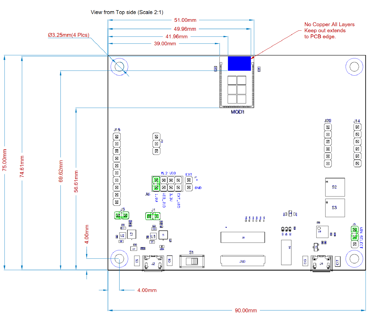
Additionally, the size of the host PCB and positioning of the Module greatly affects tuning and performance of the module antenna. The Sona NX611 1218 Chip Antenna Module has been tuned and matched to the size and position on the Host Development board shown below. Because tuning for the antenna is integrated into the module, if the reference design board size is not followed, performance of the antenna will be degraded.
Note: Please use the latest CAD files from the Ezurio web site when incorporating the Sona™ 1218 module into a new design. CAD files are provided in native Altium as well as Gerber and PDF formats.
Sona NX611 Integrated Antenna module RF Layout Guidelines
The following is a list of RF layout design guidelines and recommendation when installing an Ezurio radio into your device.
- Do not run any cables directly above or directly below the radio.
- Do not place any parts or run any high-speed digital lines below the radio.
- Ensure that there is the maximum allowable spacing separating the antenna connectors on the Ezurio radio from the antenna. In addition, do not place antennas directly above or directly below the radio.
- Ezurio recommends the use of a double-shielded cable for the connection between the radio and the antenna elements.
- Be sure to put a 10uF/16V/0603 capacitor on EACH 3.3V power pin. Also, place that capacitor as close as possible to the pin to make sure the internal PMU is working correctly.
- Use proper electro-static-discharge (ESD) procedures when installing the Ezurio radio module. To avoid negatively impacting Tx power and receiver sensitivity, do not cover the antennas with metallic objects or components.
- Ezurio’s surface mount modules are designed to conform to all major manufacturing guidelines. This application note is intended to provide additional guidance beyond the information that is presented in the user manual. This application note is considered a living document and will be updated as new information is presented.
- The modules are designed to meet the needs of commercial and industrial applications. They are easy to manufacture and conform to current automated manufacturing processes.
- The Sona NX611 Integrated antenna variant should be located at the center of the Host PCB and surrounded by ground on three sides. The antenna keep out region as defined in Figure 4must be kept clear of copper on all layers of the host PCB.
| Version | Date | Notes | Contributor(s) | Approver |
|---|---|---|---|---|
| 0.1 | 11 June 2023 | Preliminary release. | Peter Scharpf | Andy Ross |
| 1.0 | 5 Feb 2025 | Initial release | Dave Drogowski | Andy Ross |