/filters:background_color(white)/2025-12/Sona%20NX611%20-%20Family.png)
| Version | Date | Notes | Contributors | Approver |
|---|---|---|---|---|
| 0.1 | 23 March 2023 | Preliminary version. | Various | Andy Ross |
| 0.2 | 11 June 2024 | Ezurio branding. | Sue White | Dave Drogowski |
| 1.0 | 5 Feb 2025 | Initial release. | Dave Drogowski | Andy Ross |
Introduction
This document describes key hardware aspects of Ezurio’s Sona™ NX611 Wi-Fi 6 / Bluetooth 5.3 modules, which are based on NXP’s IW611 chipset. It serves as a preliminary supplement to the full module datasheet and is provided to assist in initial hardware integration.
The following are covered in this integration guide:
- Sona™ NX611 SIP Module
- Sona™ NX611 SIP Module PCB Footprint
- Sona™ NX611 SIP Module Mechanical Drawing
- Sona™ NX611 1216 Module
- Sona™ NX611 M.2 1216 Module PCB Footprint
- Sona™ NX611 M.2 1216 Module Mechanical Drawing
- Sona™ NX611 M.2 1216 Module Pinout
- Sona™ NX611 M.2 2230 Module
- Sona™ NX611 M.2 2230 Module Mechanical Drawing
- Sona™ NX611 M.2 2230 Module Pinout
- Sona™ NX611 M.2 2230 Module
Note: Data in this document is drawn from several sources and is subject to change.
 | 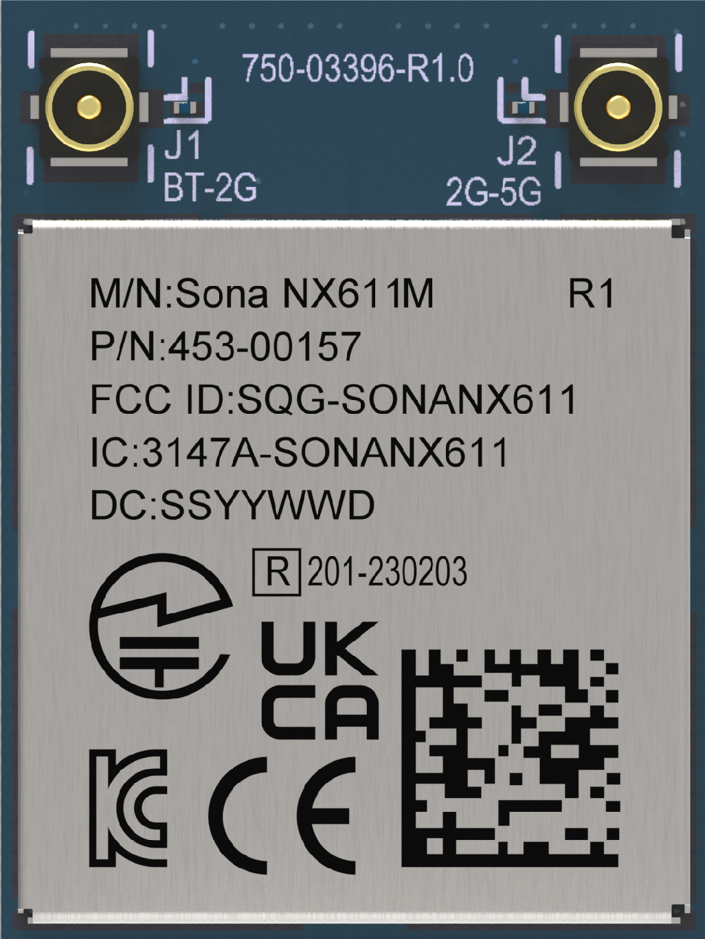 |  |
| Figure 1: Sona NX611 SIP Module | Figure 2: Sona NX611 M.2 1216 SMT Module | Figure 3: Sona NX611 M.2 2230 Module |
Sona™ NX611 SIP Module
This section describes the hardware footprint, mechanical drawing and hardware pinout of the Sona NX611 SIP module. It provides details and pin assignments critical to hardware integration of the module.
Sona™ NX611 SIP Module PCB Footprint
Module dimensions of the Sona NX611 SIP wireless module are 11 x 11 x 1.69 mm.
Sona™ NX611 SIP Module Mechanical Drawing
The Wi-Fi MAC address is located on the product label.
The last digit of Wi-Fi MAC address is assigned to either 0, 2, 4, 6, 8, A, C, E.
The Bluetooth MAC address is the Wi-Fi MAC address plus 1.
Sona™ NX611 SIP Module Pinout
Table 1: Sona NX611 SIP Module Pinout
| Pin Number | Pin Name | Description | Notes |
|---|---|---|---|
| 1 | GND | Ground | |
| 2 | VIO_SD | SDIO Power Supply | |
| 3 | GND | Ground | |
| 4 | SD_CMD | SD Command/response (input/output) | |
| 5 | SD_CLK | SD Clock input | |
| 6 | SD_DAT[1] | SD Data line bit[1] | |
| 7 | SD_DAT[3] | SD Data line bit[3] | |
| 8 | GND | Ground | |
| 9 | SD_DAT[2] | SD Data line bit[2] | |
| 10 | SD_DAT[0] | SD Data line bit[0] | |
| 11 | GPIO[21]/SD_INT | SDIO interrupt signal (output). | |
| 12 | BUCK_SENSE | Internal buck voltage. (for troubleshooting only) | |
| 13 | VIO | 1.8V/3.3V digital I/O power supply | |
| 14 | GPIO[8]/UART_CTS | UART clear-to-send input signal (active low) | |
| 15 | GPIO[10]/UART_RX | UART serial input signal. | |
| 16 | GPIO[9]/UART_RTS | UART request-to-send output signal (active low). | |
| 17 | GPIO[11]/UART_TX | UART serial output signal. | |
| 18 | GPIO[13]/EXT_REQ | External radio request input signal (COEX) | |
| 19 | GPIO[12]/EXT_STATE | External radio state input signal (COEX) | |
| 20 | GND | Ground | |
| 21 | GPIO[14]/EXT_GNT | External radio grant output signal (COEX) | |
| 22 | GPIO[15]/EXT_PRI | External radio input priority signal (COEX) | |
| 23 | GPIO[0]/XOSC_EN | Oscillator enable (output) | |
| 24 | GPIO[20]/EXT_FREQ | External radio frequency input signal (COEX) | |
| 25 | CONFIG_HOST[1] | NC | |
| 26 | CONFIG_HOST[0] | NC | |
| 27 | GND | Ground | |
| 28 | GPIO[4]/PCM_CLK | PCM data clock (output if master, input if slave) | |
| 29 | GPIO[3]/PCM_MCLK | PCM clock output signal (optional) | |
| 30 | GPIO[5]/PCM_DOUT | PCM transmit data signal (output) | |
| 31 | GPIO[6]/PCM_DIN | PCM receive data signal (input) | |
| 32 | GPIO[7]/PCM_SYNC | PCM frame sync (output if master, input if slave) | |
| 33 | GPIO[2]/IND_RST_BT | Independent software reset for Bluetooth (input) | |
| 34 | GPIO[1]/IND_RST_WL | Independent software reset for Wi-Fi (input) | |
| 35 | GND | Ground | |
| 36 | AVDD18 | 1.8V analog power supply | Module has a weak 51K Ω Pull Up to 3.3V. For increased noise and ESD immunity, connect to host output pin. |
| 37 | AVDD18 | 1.8V analog power supply | |
| 38 | GND | Ground | |
| 39 | GND | Ground | |
| 40 | PDn | Full Power-down (input) (active low) | |
| 41 | GND | Ground | |
| 42 | GND | Ground | |
| 43 | GND | Ground | |
| 44 | RF_TR_5 | Wi-Fi transmit/receive (5 GHz) | |
| 45 | GND | Ground | |
| 46 | AVDD33 | 3.3V analog power supply | |
| 47 | AVDD33 | 3.3V analog power supply | |
| 48 | GND | Ground | |
| 49 | GND | Ground | |
| 50 | GND | Ground | |
| 51 | GND | Ground | |
| 52 | BRF_ANT | Bluetooth radio transmit/receive interface | |
| 53 | GND | Ground | |
| 54 | GND | Ground | |
| 55 | GND | Ground | |
| 56 | GPIO[26]/WCI-2_SOUT | Receive signal from external radio (input) (COEX) | |
| 57 | GPIO[25]/WCI-2_SIN | Transmit signal to external radio (output) (COEX) | |
| 58 | GND | Ground | |
| 59 | RF_CNTL4 | RF control line 4 | |
| 60 | RF_CNTL3 | RF control line 3 | |
| 61 | RF_CNTL2 | RF control line 2 | |
| 62 | RF_CNTL1 | RF control line 1 | |
| 63 | RF_CNTL0 | RF control line 0 | |
| 64 | GPIO[18]/BT_WAKE_IN | ||
| 65 | GPIO[19]/BT_WAKE_OUT | Bluetooth wake-up signal (output). | |
| 66 | GPIO[17]/WL_WAKE_OUT | Wi-Fi radio wake-up signal (output). | |
| 67 | GPIO[16]/WL_WAKE_IN | Wi-Fi radio wake-up signal (input) | |
| 68 | GND | Ground | |
| 69 | GPIO[22] | I/O | |
| 70 | GPIO[23] | I/O | |
| 71 | GPIO[24] | I/O | |
| 72 | GPIO[27] | I/O | |
| 73 | GPIO[29]/JTAG_TMS | JTAG controller select (input) | |
| 74 | GPIO[31]/JTAG_TDO | JTAG test data signal (output) | |
| 75 | GPIO[28]/JTAG_TCK | JTAG test clock signal (input) | |
| 76 | GPIO[30]/JTAG_TDI | JTAG test data signal (input) | |
| G1 | GND | Ground |
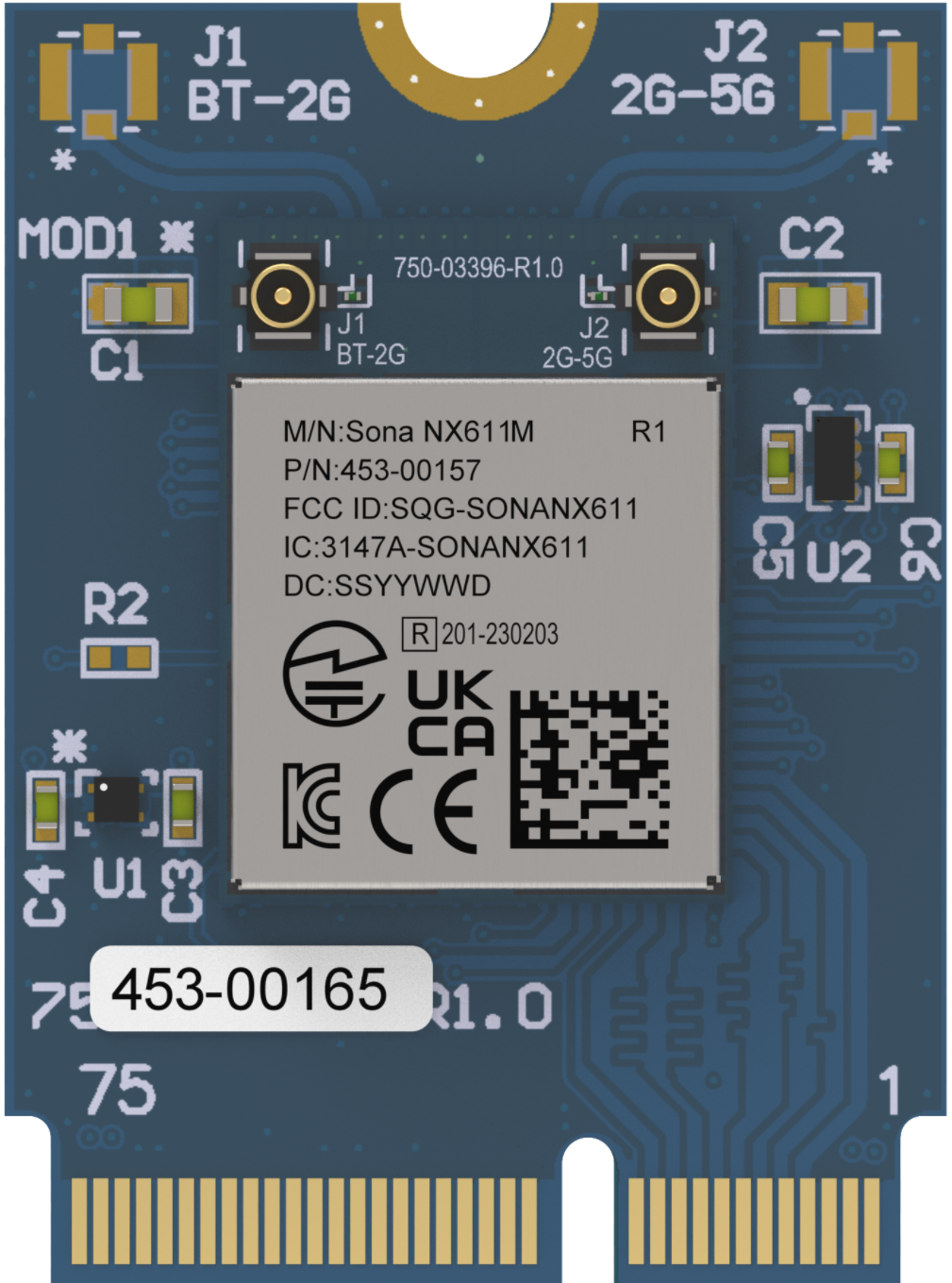
Sona™ NX611 1216 Module
This section describes the hardware footprint, mechanical drawing and hardware pinout of the Sona NX611 M.2 1216 module. It provides details and pin assignments critical to hardware integration of the module.
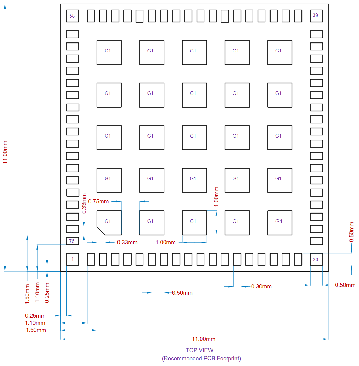
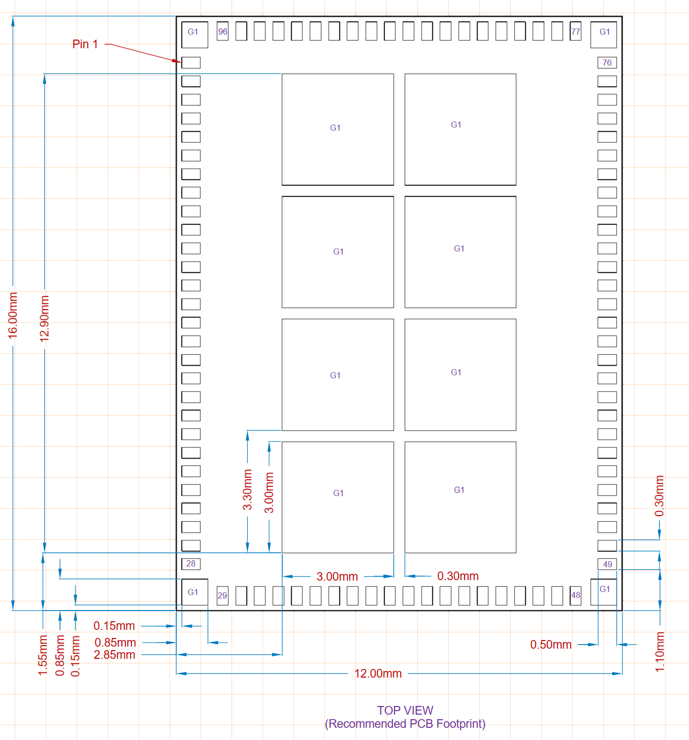
Sona™ NX611 M.2 1216 Module PCB Footprint
Module dimensions of the Sona NX611 M.2 1216 wireless module are 12 x 16 x 1.72 mm
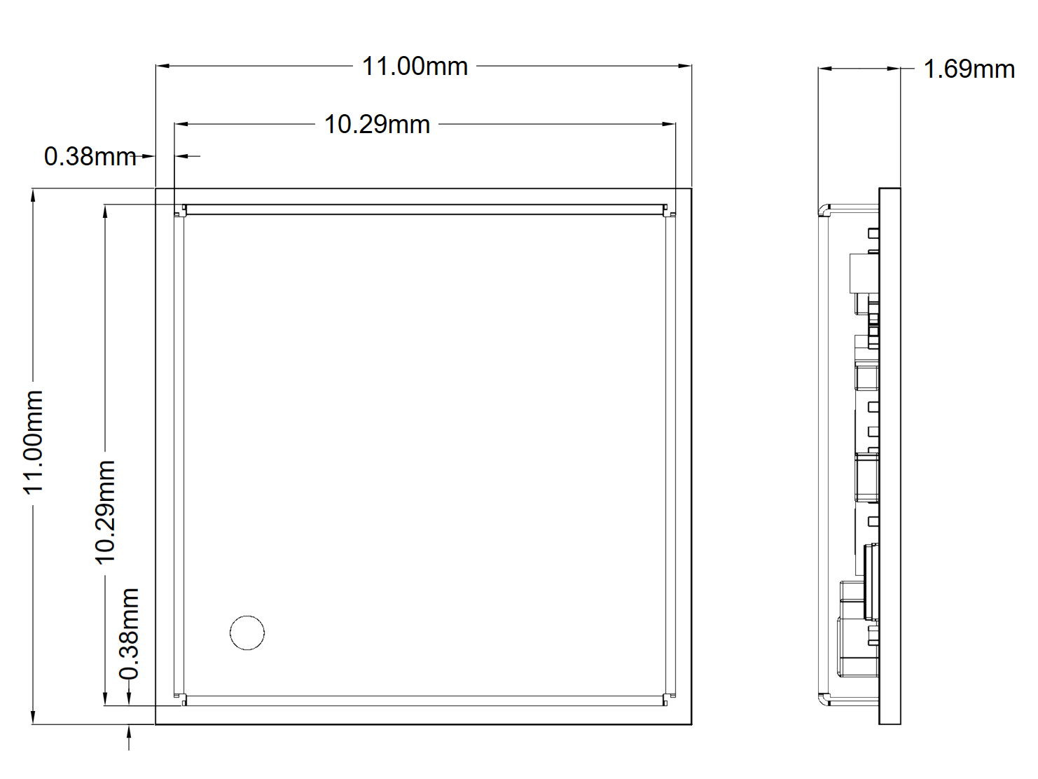
Sona™ NX611 M.2 1216 Module Mechanical Drawing
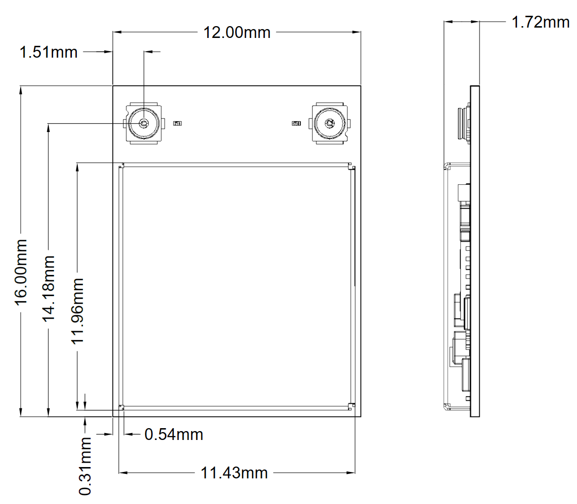
Figure 7: Mechanical Drawing – NX611 M.2 1216 module
The Wi-Fi MAC address is located on the product label.
The last digit of Wi-Fi MAC address is assigned to either 0, 2, 4, 6, 8, A, C, E.
The Bluetooth MAC address is the Wi-Fi MAC address plus 1.
Sona™ NX611 M.2 1216 Module Pinout
Table 2: Sona NX611 M.2 1216 Module Pinout
| Pin Number | PCIe M.2 Name | Pin Name NX611 | Description |
|---|---|---|---|
| 1 | UIM_POWER_SRC/GPIO1 | UNUSED | |
| 2 | UIM_POWER_SNK | UNUSED | |
| 3 | UIM_SWP | UNUSED | |
| 4 | 3.3V | 3.3V | |
| 5 | 3.3V | 3.3V | |
| 6 | GND | Ground | Ground |
| 7 | RESERVED | UNUSED | |
| 8 | ALERT# | NC | |
| 9 | I2C_CLK | NC | |
| 10 | I2C_DATA | NC | |
| 11 | COEX_RXD | COEX_RXD | |
| 12 | COEX_TXD | COEX_TXD | |
| 13 | COEX3 | UNUSED | |
| 14 | SYSCLK/GNSS_0 | UNUSED | |
| 15 | TX_BLANKING/GNSS_1 | UNUSED | |
| 16 | RESERVED | UNUSED | |
| 17 | GND | Ground | Ground |
| 18 | RESERVED | UNUSED | |
| 19 | RESERVED | NC | |
| 20 | GND | Ground | Ground |
| 21 | PETn1 | UNUSED | |
| 22 | PETp1 | UNUSED | |
| 23 | GND | Ground | |
| 24 | PERn1 | UNUSED | |
| 25 | PERp1 | UNUSED | |
| 26 | GND | Ground | |
| 27 | SUSCLK(32kHz) | UNUSED | |
| 28 | W_DISABLE1# | PDn | Module has a weak 51K Ω Pull Up to 3.3V. For increased noise and ESD immunity, connect to host output pin. |
| 29 | PEWAKE# | UNUSED | |
| 30 | CLKREQ# | UNUSED | |
| 31 | PERST# | UNUSED | |
| 32 | GND | Ground | Ground |
| 33 | REFCLKn0 | UNUSED | |
| 34 | REFCLKp0 | UNUSED | |
| 35 | GND | Ground | Ground |
| 36 | PETn0 | UNUSED | |
| 37 | PETp0 | UNUSED | |
| 38 | GND | Ground | Ground |
| 39 | PERn0 | UNUSED | |
| 40 | PERp0 | UNUSED | |
| 41 | GND | Ground | Ground |
| 42 | VENDOR DEFINED | EXT_PRI | |
| 43 | VENDOR DEFINED | BT_WAKE_IN | |
| 44 | VENDOR DEFINED | WL_WAKE_IN | |
| 45 | SDIO RESET# | IND_RST_WL | |
| 46 | SDIO WAKE# | WL_WAKE_OUT | |
| 47 | SDIO DATA3 | SDIO DATA3 | |
| 48 | SDIO DATA2 | SDIO DATA2 | |
| 49 | SDIO DATA1 | SDIO DATA1 | |
| 50 | SDIO DATA0 | SDIO DATA0 | |
| 51 | SDIO CMD | SDIO CMD | |
| 52 | SDIO CLK | SDIO CLK | |
| 53 | UART WAKE# | BT_WAKE_OUT | |
| 54 | UART CTS | UART CTS | |
| 55 | UART Tx | UART Tx | |
| 56 | UART Rx | UART Rx | |
| 57 | UART RTS | UART RTS | |
| 58 | PCM_SYNC/I2S_WS | PCM_SYNC/I2S_WS | |
| 59 | PCM_IN/I2S_SD_IN | PCM_IN/I2S_SD_IN | |
| 60 | PCM_OUT/I2S_SD_OUT | PCM_OUT/I2S_SD_OUT | |
| 61 | PCM_CLK/I2S_SCK | PCM_CLK/I2S_SCK | |
| 62 | GND | Ground | Ground |
| 63 | W_DISABLE2# | IND_RST_BT | |
| 64 | LED_2# | UNUSED | |
| 65 | LED_1# | UNUSED | |
| 66 | RESERVED/VIO_1.8 | VIO_1.8 | |
| 67 | RESERVED | UNUSED | |
| 68 | GND | Ground | Ground |
| 69 | USB_D- | UNUSED | |
| 70 | USB_D+ | UNUSED | |
| 71 | GND | Ground | Ground |
| 72 | 3.3V | 3.3V | |
| 73 | 3.3V | 3.3V | |
| 74 | GND | Ground | Ground |
| 75 | GND | Ground | Ground |
| 76 | GND/VIO_CFG | NC | |
| 77 | GND | Ground | Ground |
| 78 | GND | Ground | Ground |
| 79 | GND | Ground | Ground |
| 80 | GND | Ground | Ground |
| 81 | WL_C2 | Bluetooth RF Out | |
| 82 | GND | Ground | Ground |
| 83 | GND | Ground | Ground |
| 84 | GND | Ground | Ground |
| 85 | GND | Ground | Ground |
| 86 | WL_C0 | 5G_2.4G WiFi RF Out (Shared WiFi and Bluetooth, single trace Pad variant) | |
| 87 | GND | Ground | Ground |
| 88 | GND | Ground | Ground |
| 89 | GND | Ground | Ground |
| 90 | GND | Ground | Ground |
| 91 | GND | Ground | Ground |
| 92 | WL_C1 | UNUSED | |
| 93 | GND | Ground | Ground |
| 94 | GND | Ground | Ground |
| 95 | GND | Ground | Ground |
| 96 | GND | Ground | Ground |
| G1 | GND | Ground | Ground |
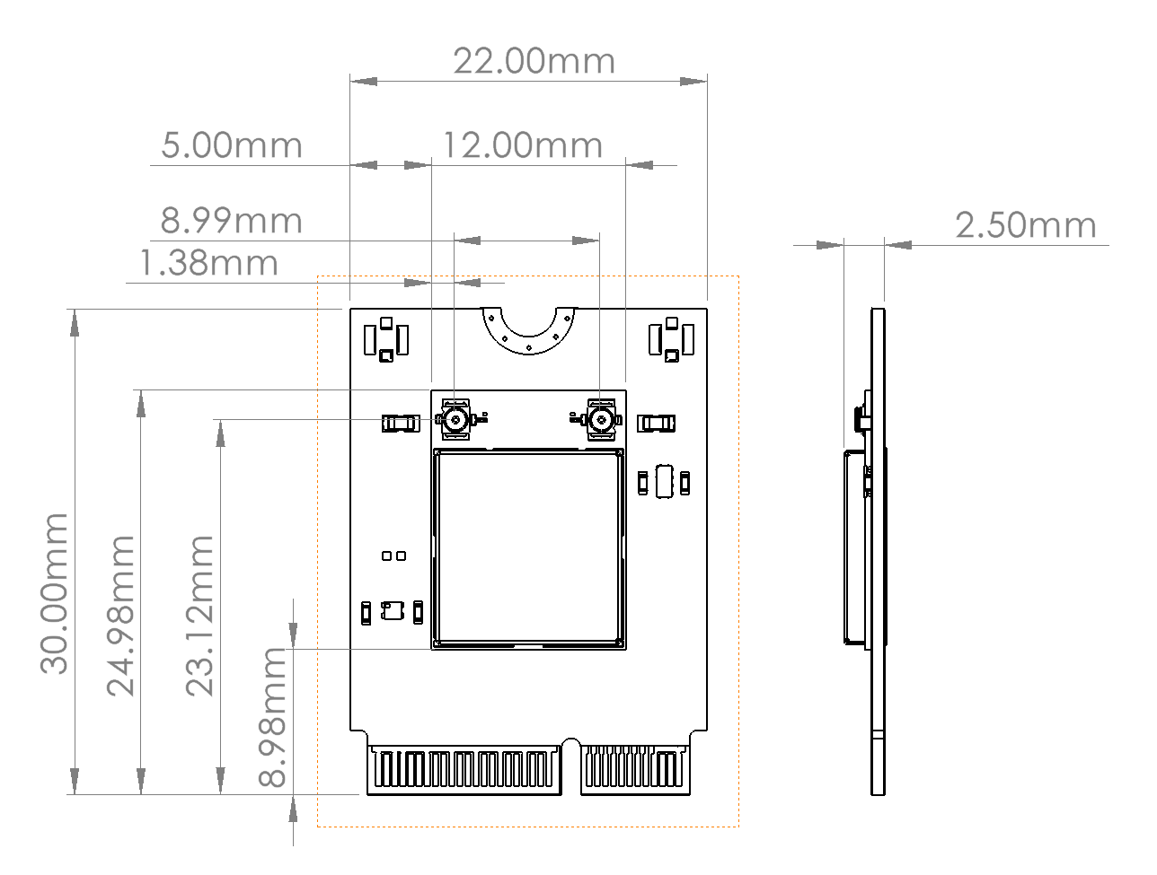
Sona™ NX611 M.2 2230 Module
This section describes the hardware footprint, mechanical drawing and hardware pinout of the NX611 M.2 2230 module. It provides details and pin assignments critical to hardware integration of the module.
Sona™ NX611 M.2 2230 Module Mechanical Drawing
The Wi-Fi MAC address is located on the product label.
The last digit of Wi-Fi MAC address is assigned to either 0, 2, 4, 6, 8, A, C, E.
The Bluetooth MAC address is the Wi-Fi MAC address plus 1.
Sona™ NX611 M.2 2230 Module Pinout
Table 3: Sona NX611 M.2 2230 Module Pinout
| Pin # | PCIe M.2 Name | Pin Name NX611 |
| 1 | GND | GND |
| 2 | 3.3 V | 3.3 V |
| 3 | USB_D+ | USB_D+ |
| 4 | 3.3 V | 3.3 V |
| 5 | USB_D- | USB_D- |
| 6 | LED_1# (I)(OD) | LED_1# (I)(OD) |
| 7 | GND | GND |
| 8 | PCM_CLK/I2S_SCK (I/O)(0/1.8V) | PCM_CLK/I2S_SCK (I/O)(0/1.8V) |
| 9 | SDIO_CLK/SYSCLK (I) (0/1.8V) | SDIO_CLK/SYSCLK (I) (0/1.8V) |
| 10 | PCM_SYNC/I2S_WS (I/O)(0/1.8V) | PCM_SYNC/I2S_WS (I/O)(0/1.8V) |
| 11 | SDIO_CMD (I/O) (0/1.8V) | SDIO_CMD (I/O) (0/1.8V) |
| 12 | PCM_OUT/I2S_SD_OUT (O)(0/1.8V) | PCM_OUT/I2S_SD_OUT (O)(0/1.8V) |
| 13 | SDIO_DATA0 (I/O) (0/1.8V) | SDIO_DATA0 (I/O) (0/1.8V) |
| 14 | PCM_IN/I2S_SD_IN (I)(0/1.8V) | PCM_IN/I2S_SD_IN (I)(0/1.8V) |
| 15 | SDIO_DATA1 (I/O) (0/1.8V) | SDIO_DATA1 (I/O) (0/1.8V) |
| 16 | LED_2# (I)(OD) | LED_2# (I)(OD) |
| 17 | SDIO_DATA2 (I/O) (0/1.8V) | SDIO_DATA2 (I/O) (0/1.8V) |
| 18 | VIO_CFG/GND | VIO_CFG/GND |
| 19 | SDIO_DATA3 (I/O) (0/1.8V) | SDIO_DATA3 (I/O) (0/1.8V) |
| 20 | BT_15.4_WAKE_OUT | BT_15.4_WAKE_OUT |
| 21 | WL_WAKE_OUT: | WL_WAKE_OUT: |
| 22 | UART_RXD (I)(0/1.8V) | UART_RXD (I)(0/1.8V) |
| 23 | IND_RST_WL(I) | IND_RST_WL(I) |
| 24-31 | CONNECTOR KEY E | CONNECTOR KEY E |
| 32 | UART_RXD (I)(0/1.8V) | UART_RXD (I)(0/1.8V) |
| 33 | GND | GND |
| 34 | UART_RTS (O)(0/1.8V) | UART_RTS (O)(0/1.8V) |
| 35 | PETp0 | PETp0 |
| 36 | UART_CTS (I)(0/1.8V) | UART_CTS (I)(0/1.8V) |
| 37 | PERn0 | PERn0 |
| 38 | NC | NC |
| 39 | GND | GND |
| 40 | WL_WAKE_IN | WL_WAKE_IN |
| 41 | PETp0 | PETp0 |
| 42 | BT_WAKE_IN | BT_WAKE_IN |
| 43 | PETn0 | PETn0 |
| 44 | COEX3 (I/O)(0/1.8V) | COEX3 (I/O)(0/1.8V) |
| 45 | GND | GND |
| 46 | COEX_TXD (O)(0/1.8V) | COEX_TXD (O)(0/1.8V) |
| 47 | REFCLKp0 | REFCLKp0 |
| 48 | COEX_RXD (I)(0/1.8V) | COEX_RXD (I)(0/1.8V) |
| 49 | REFCLKn0 | REFCLKn0 |
| 50 | SUSCLK (I)( 0/1.8V/3.3V) | SUSCLK (I)( 0/1.8V/3.3V) |
| 51 | GND | GND |
| 52 | PERST0# (I)( 0/1.8V/3.3V) | PERST0# (I)( 0/1.8V/3.3V) |
| 53 | CLKREQ0# (I/O)( 0/1.8V/3.3V) | CLKREQ0# (I/O)( 0/1.8V/3.3V) |
| 54 | IND_RST_BT (I) | IND_RST_BT (I) |
| 55 | PEWAKE0# (I/O)( 0/1.8V/3.3V) | PEWAKE0# (I/O)( 0/1.8V/3.3V) |
| 56 | PDn (I) | PDn (I) |
| 57 | GND | GND |
| 58 | NC | NC |
| 59 | RESERVED | RESERVED |
| 60 | NC | NC |
| 61 | RESERVED | RESERVED |
| 62 | NC | NC |
| 63 | GND | GND |
| 64 | RESERVED/VIO 1.8V | RESERVED/VIO 1.8V |
| 65 | RESERVED | RESERVED |
| 66 | UIM_SWP/PERST1# | UIM_SWP/PERST1# |
| 67 | RESERVED | RESERVED |
| 68 | UIM_POWER_SNK/CLKREQ1# | UIM_POWER_SNK/CLKREQ1# |
| 69 | GND | GND |
| 70 | UIM_POWER_SRC/ GPIO_1/PEWAKE1# | UIM_POWER_SRC/ GPIO_1/PEWAKE1# |
| 71 | RESERVED | RESERVED |
| 72 | 3.3 V | 3.3 V |
| 73 | RESERVED | RESERVED |
| 74 | 3.3 V | 3.3 V |
| 75 | GND | GND |
FCC Modular Certification Requirements
Because these modules and their associated set of approved antennas has been certified by the FCC and Industry Canada (IC) as Modular Radios, the end user is authorized to integrate this module into an end-product and is solely responsible for the Unintentional Emissions levels produced by the end-product.
To uphold the Modular Radio certifications, the integrator of the module must abide by the PCB layout recommendations outlined in the following paragraphs. Any divergence from these recommendations will invalidate the modular radio certifications and require the integrator to re-certify the module and/or end-product.
The module must be used with one of the approved antennas:
Table 4: Sona Approved Antennas
| Manufacturer | Model | Ezurio Part Number | Type | Connector | 2.4GHz | 5GHz | 5.6GHz |
|---|---|---|---|---|---|---|---|
| Ezurio | FlexMIMO 6E | EFD2471A3S-10MH4L | PIFA | IPEX MHF4L | 2.2dBi | 3.8dBi | 3.3dBi |
| Ezurio | FlexPIFA 6E | EFB2471A3S-10MH4L | PIFA | IPEX MHF4L | 2.2dBi | 3.9dBi | 3.8dBi |
| Ezurio | Mini NanoBlade Flex 6E | EMF2471A3S-10MH4L | PCB Dipole | IPEX MHF4L | 2.4dBi | 4.4dBi | 5.2dBi |
| Ezurio | FlexPIFA | 001-0021 | PIFA | IPEX MHF4L | 2.5dBi | 3.0dBi | |
| JOYMAX | Dipole 6E | TWX-100BRSAX-2001 | Dipole | RP-SMA | 2dBi | 4dBi | 4dBi |
When using the module and the reference design that supports the off module MH4 connector(s), you may use a substitute antenna if it is of the same type and that the gain is less than or equal to the smallest gain for that type for each of the frequencies listed.
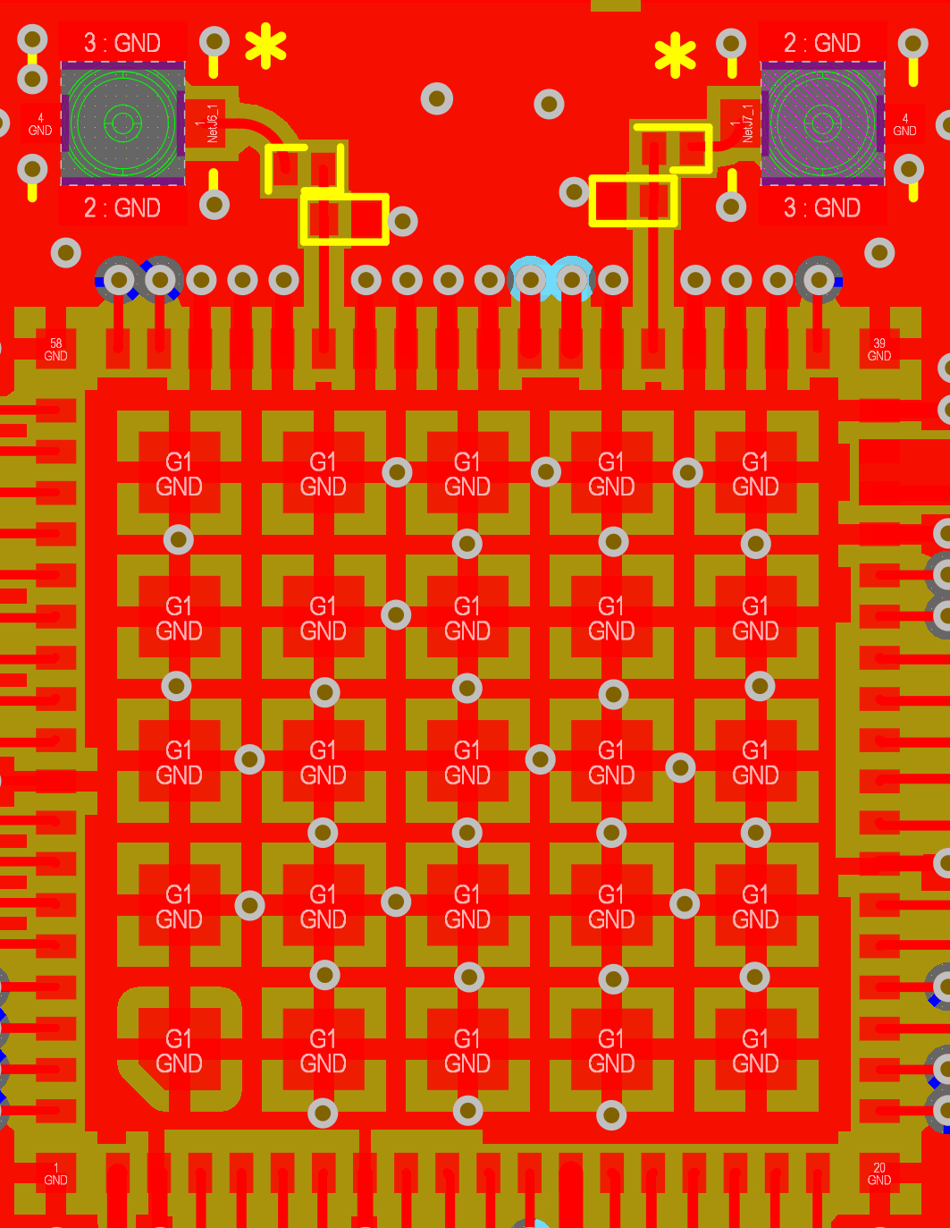
Ezurio provides a FCC Modular Certified reference design. It is a controlled impedance PCB that uses microstrip trace design to route RF signals from the module to the coaxial connectors.
Please use the latest CAD files from the Ezurio web site when incorporating the Sona™ module into a new design. CAD files are provided in native Altium as well as Gerber and PDF formats.
Sona NX611 SIP Certified Module Host Board Requirements
Table 5: Sona NX611 SIP Modules
| Part Number | Description |
|---|---|
| 453-00155 | Module, Sona NX611 SIP, 2 RF Trace Pin |
| 453-00156 | Module, Sona NX611 SIP, 1 RF Trace Pin |
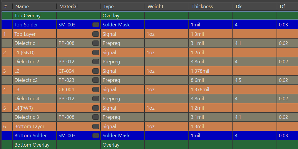
The reference design for the Ezurio Sona NX611 SIP Module has been integrated into the Sona NX611 Development Board. It is 6-layer PCB with a total thickness of 0.79mm. The reference design includes designs for the singe port version as well as the dual port version.
To comply with FCC regulations, the RF area of host design must match the RF area of the reference design exactly. To match exactly, the distance from the top layer to the RF reference ground plane on host PCB and the Dk of the host board must match the Reference design. When the reference ground plane and Dk of the host board match, the 50 ohm RF trace widths will be the same and the host board copper can match the reference board copper.

Note: Please use the latest CAD files from the Ezurio web site when incorporating the Sona™ module into a new design. CAD files are provided in native Altium as well as Gerber and PDF formats.
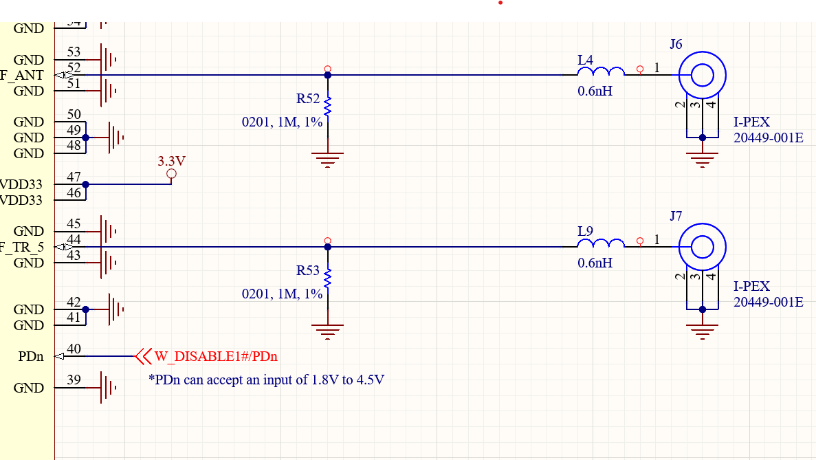
In addition to matching the reference design layout, there are several RF critical BOM components in the reference design that cannot be substituted shown in Table 6.
Table 6: RF Critical Components BOM
| PCB Ref | Value | Manufacturer | Mfg Part Number | Alt. Manufacturer | Alt. Mfg Part Number |
|---|---|---|---|---|---|
| L4, L9 | 0.6nH | Murata | LQP03TN0N6B02D | - | - |
| J6, J7 | MH4 | I-PEX | 20449-001E | Taoglas | 20449.001E-01 |
* RF Critical Components That Cannot be Substituted
Sona™ NX611 M.2 2230 Module Mounting Guidelines
The Sona NX611 M.2 2230 module connects to the host via a standard PCI EXPRESS M2 connector. The Kyocera (www.Kyocera-connector.com) 6411 series provides 1.8 mm, 2.3 mm and 3.2 mm connector heights and the JAE (https://www.jae.com/en/) SM3 series provides 1.2 mm, 2.15 mm, 3.1 mm and 4.1 mm connector heights.
Because the Sona NX611 M.2 module is a single-side component module, we recommend the following part numbers which have 2.3 mm and 3.1 mm connector height:
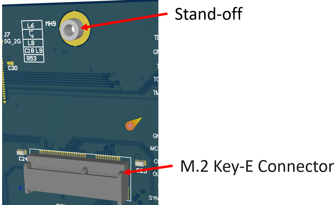
| M.2 Key-E Connector | Connector Height | Stand-off |
|---|---|---|
| KYOCERA 24-6411-067-101-894E | 2.3 mm | EMI STOP F50M16-041525P1D4M |
| JAE SM3ZS067U310AERxxxx | 3.1 mm | JAE SM3ZS067U310-NUT1-Rxxxx |
Regulatory
Note: For complete regulatory information, refer to the Sona™ NX61X Regulatory Information document (coming soon) which is also available from the Sona™ NX61X product page.
The Sona™ NX61X holds current certifications in the following countries:
Table 7: Sona™NX61X countries with certification (SIP)
| Country/Region | Regulatory ID |
|---|---|
| USA (FCC) | SQG-SonaNX611S |
| EU | No Regulatory ID Required |
| Canada (ISED) | 3147A-SonaNX611S |
| Japan (MIC) | TBD |
| Australia | No Regulatory ID Required |
| New Zealand | No Regulatory ID Required |
Table 8: Sona™NX61X countries with certification (M.2 1216 Module and M.2 2230 Module)
| Country/Region | Regulatory ID |
|---|---|
| USA (FCC) | SQG-SonaNX611M |
| EU | No Regulatory ID Required |
| Canada (ISED) | 3147A-SonaNX611M |
| Japan (MIC) | TBD |
| Australia | No Regulatory ID Required |
| New Zealand | No Regulatory ID Required |